EL5211A
®
Data Sheet
July 23, 2009
60MHz Rail-to-Rail Input-Output Op Amp
Features
The EL5211A is a low power, high voltage, rail-to-rail
input-output amplifier. The EL5211A contains two amplifiers.
Operating on nominal supplies ranging from 5V to 15V while
consuming only 2.5mA per amplifier, the EL5211A has a
bandwidth of 60MHz (-3dB) and provides common-mode
input ability beyond the supply rails, as well as rail-to-rail
output capability. This enables the EL5211A to offer
maximum dynamic range at any supply voltage.
• 60MHz (-3dB) bandwidth
The EL5211A also features fast slewing and settling times,
as well as a high continuous output drive capability of 65mA
(sink and source). These features make the EL5211A ideal
for high speed filtering and signal conditioning application.
Other applications include battery-powered, portable devices
and anywhere low power consumption is important.
• Rail-to-rail output swing
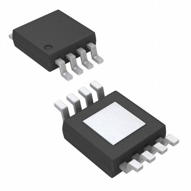
The EL5211A is available in the 8 Ld HMSOP package,
features a standard operational amplifier pinout, and is
specified for operation over a temperature range of -40°C to
+85°C.
• TFT-LCD panels
FN6143.2
• Supply voltage = 4.5V to 16.5V
• Low supply current (per amplifier) = 2.5mA
• High slew rate = 75V/µs
• Unity-gain stable
• Beyond the rails input capability
• ±110mA output short current
• Pb-free (RoHS compliant)
Applications
• VCOM amplifiers
• Drivers for A/D converters
• Data acquisition
Ordering Information
PART NUMBER
(Note)
PART
MARKING
• Video processing
PACKAGE
(Pb-free)
PKG.
DWG. #
EL5211AIYEZ
BBLAA
8 Ld HMSOP
(3.0mm)
MDP0050
EL5211AIYEZ-T7*
BBLAA
8 Ld HMSOP
(3.0mm)
MDP0050
EL5211AIYEZ-T13*
BBLAA
8 Ld HMSOP
(3.0mm)
MDP0050
• Audio processing
• Active filters
• Test equipment
• Battery-powered applications
• Portable equipment
Pinout
*Please refer to TB347 for details on reel specifications.
NOTE: These Intersil Pb-free plastic packaged products employ
special Pb-free material sets, molding compounds/die attach
materials, and 100% matte tin plate plus anneal (e3 termination
finish, which is RoHS compliant and compatible with both SnPb and
Pb-free soldering operations). Intersil Pb-free products are MSL
classified at Pb-free peak reflow temperatures that meet or exceed
the Pb-free requirements of IPC/JEDEC J STD-020.
EL5211A
(8 LD HMSOP)
TOP VIEW
VOUTA 1
VINA- 2
VINA+ 3
VS- 4
1
8 VS+
7 VOUTB
+
+
6 VINB5 VINB+
CAUTION: These devices are sensitive to electrostatic discharge; follow proper IC Handling Procedures.
1-888-INTERSIL or 1-888-468-3774 | Intersil (and design) is a registered trademark of Intersil Americas Inc.
Copyright © Intersil Americas Inc. 2005, 2007, 2009. All Rights Reserved.
All other trademarks mentioned are the property of their respective owners.
�EL5211A
Absolute Maximum Ratings (TA = +25°C)
Thermal Information
Supply Voltage between VS+ and VS- . . . . . . . . . . . . . . . . . . . .+18V
Input Voltage . . . . . . . . . . . . . . . . . . . . . . . . . . VS- - 0.5V, VS +0.5V
Maximum Continuous Output Current . . . . . . . . . . . . . . . . . . ±65mA
Storage Temperature . . . . . . . . . . . . . . . . . . . . . . . .-65°C to +150°C
Ambient Operating Temperature . . . . . . . . . . . . . . . .-40°C to +85°C
Maximum Die Temperature . . . . . . . . . . . . . . . . . . . . . . . . . . +150°C
Power Dissipation . . . . . . . . . . . . . . . . . . . . . . . . . . . . . See Curves
Pb-Free Reflow Profile. . . . . . . . . . . . . . . . . . . . . . . . .see link below
http://www.intersil.com/pbfree/Pb-FreeReflow.asp
CAUTION: Do not operate at or near the maximum ratings listed for extended periods of time. Exposure to such conditions may adversely impact product reliability and
result in failures not covered by warranty.
IMPORTANT NOTE: All parameters having Min/Max specifications are guaranteed. Typ values are for information purposes only. Unless otherwise noted, all tests are
at the specified temperature and are pulsed tests, therefore: TJ = TC = TA
Electrical Specifications
PARAMETER
VS+ = +5V, VS- = -5V, RL = 1kΩ to 0V, TA = +25°C, Unless Otherwise Specified. Parameters with MIN and/or
MAX limits are 100% tested at +25°C, unless otherwise specified. Temperature limits established by
characterization and are not production tested.
DESCRIPTION
CONDITIONS
MIN
TYP
MAX
UNIT
3
15
mV
INPUT CHARACTERISTICS
VOS
Input Offset Voltage
TCVOS
Average Offset Voltage Drift (Note 1)
IB
Input Bias Current
RIN
Input Impedance
1
GΩ
CIN
Input Capacitance
2
pF
CMIR
Common-Mode Input Range
CMRR
Common-Mode Rejection Ratio
for VIN from -5.5V to 5.5V
50
70
dB
AVOL
Open-Loop Gain
-4.5V ≤ VOUT ≤ 4.5V
60
70
dB
VCM = 0V
7
VCM = 0V
2
-5.5
µV/°C
60
+5.5
nA
V
OUTPUT CHARACTERISTICS
VOL
Output Swing Low
IL = -5mA
VOH
Output Swing High
IL = 5mA
ISC
IOUT
-4.9
4.8
-4.8
V
4.9
V
Short-Circuit Current
±110
mA
Output Current
±65
mA
80
dB
POWER SUPPLY PERFORMANCE
PSRR
Power Supply Rejection Ratio
VS is moved from ±2.25V to ±7.75V
IS
Supply Current
No load
5
60
7.5
mA
DYNAMIC PERFORMANCE
SR
Slew Rate (Note 2)
-4.0V ≤ VOUT ≤ 4.0V, 20% to 80%
75
V/µs
tS
Settling to +0.1% (AV = +1)
(AV = +1), VO = 2V step
80
ns
BW
-3dB Bandwidth
60
MHz
GBWP
Gain-Bandwidth Product
32
MHz
PM
Phase Margin
50
°
CS
Channel Separation
f = 5MHz
110
dB
dG
Differential Gain (Note 3)
RF = RG = 1kΩ and VOUT = 1.4V
0.17
%
dP
Differential Phase (Note 3)
RF = RG = 1kΩ and VOUT = 1.4V
0.24
°
NOTES:
1. Measured over operating temperature range.
2. Slew rate is measured on rising and falling edges.
3. NTSC signal generator used.
2
FN6143.2
July 23, 2009
�EL5211A
Electrical Specifications
PARAMETER
VS+ = +5V, VS- = 0V, RL = 1kΩ to 2.5V, TA = +25°C, Unless Otherwise Specified. Parameters with MIN and/or
MAX limits are 100% tested at +25°C, unless otherwise specified. Temperature limits established by
characterization and are not production tested.
DESCRIPTION
CONDITION
MIN
TYP
MAX
UNIT
3
15
mV
INPUT CHARACTERISTICS
VOS
Input Offset Voltage
TCVOS
Average Offset Voltage Drift (Note 4)
IB
Input Bias Current
RIN
Input Impedance
1
GΩ
CIN
Input Capacitance
2
pF
CMIR
Common-Mode Input Range
CMRR
Common-Mode Rejection Ratio
for VIN from -0.5V to 5.5V
45
66
dB
AVOL
Open-Loop Gain
0.5V ≤ VOUT ≤ 4.5V
60
70
dB
VCM = 2.5V
7
VCM = 2.5V
2
-0.5
µV/°C
60
+5.5
nA
V
OUTPUT CHARACTERISTICS
VOL
Output Swing Low
IL = -5mA
VOH
Output Swing High
IL = 5mA
ISC
IOUT
100
4.8
200
mV
4.9
V
Short-Circuit Current
±110
mA
Output Current
±65
mA
80
dB
POWER SUPPLY PERFORMANCE
PSRR
Power Supply Rejection Ratio
VS is moved from 4.5V to 15.5V
IS
Supply Current
No load
5
60
7.5
mA
DYNAMIC PERFORMANCE
SR
Slew Rate (Note 5)
1V ≤ VOUT ≤ 4V, 20% to 80%
75
V/µs
tS
Settling to +0.1% (AV = +1)
(AV = +1), VO = 2V step
80
ns
BW
-3dB Bandwidth
60
MHz
GBWP
Gain-Bandwidth Product
32
MHz
PM
Phase Margin
50
°
CS
Channel Separation
f = 5MHz
110
dB
dG
Differential Gain (Note 6)
RF = RG = 1kΩ and VOUT = 1.4V
0.17
%
dP
Differential Phase (Note 6)
RF = RG = 1kΩ and VOUT = 1.4V
0.24
°
NOTES:
4. Measured over operating temperature range.
5. Slew rate is measured on rising and falling edges.
6. NTSC signal generator used.
Electrical Specifications
PARAMETER
VS+ = +15V, VS- = 0V, RL = 1kΩ to 7.5V, TA = +25°C, Unless Otherwise Specified. Parameters with MIN and/or
MAX limits are 100% tested at +25°C, unless otherwise specified. Temperature limits established by
characterization and are not production tested.
DESCRIPTION
CONDITION
MIN
TYP
MAX
UNIT
3
15
mV
INPUT CHARACTERISTICS
VOS
Input Offset Voltage
TCVOS
Average Offset Voltage Drift (Note 7)
IB
Input Bias Current
RIN
Input Impedance
3
VCM = 7.5V
7
VCM = 7.5V
2
1
µV/°C
60
nA
GΩ
FN6143.2
July 23, 2009
�EL5211A
Electrical Specifications
PARAMETER
VS+ = +15V, VS- = 0V, RL = 1kΩ to 7.5V, TA = +25°C, Unless Otherwise Specified. Parameters with MIN and/or
MAX limits are 100% tested at +25°C, unless otherwise specified. Temperature limits established by
characterization and are not production tested. (Continued)
DESCRIPTION
CONDITION
MIN
TYP
MAX
UNIT
CIN
Input Capacitance
2
pF
CMIR
Common-Mode Input Range
CMRR
Common-Mode Rejection Ratio
for VIN from -0.5V to 15.5V
53
72
dB
AVOL
Open-Loop Gain
0.5V ≤ VOUT ≤ 14.5V
60
70
dB
-0.5
+15.5
V
OUTPUT CHARACTERISTICS
VOL
Output Swing Low
IL = -5mA
VOH
Output Swing High
IL = 5mA
ISC
IOUT
100
14.8
200
mV
14.9
V
Short-Circuit Current
±110
mA
Output Current
±65
mA
80
dB
POWER SUPPLY PERFORMANCE
PSRR
Power Supply Rejection Ratio
VS is moved from 4.5V to 15.5V
IS
Supply Current
No load
5
60
7.5
mA
DYNAMIC PERFORMANCE
SR
Slew Rate (Note 8)
1V ≤ VOUT ≤ 14V, 20% to 80%
75
V/µs
tS
Settling to +0.1% (AV = +1)
(AV = +1), VO = 2V step
80
ns
BW
-3dB Bandwidth
60
MHz
GBWP
Gain-Bandwidth Product
32
MHz
PM
Phase Margin
50
°
CS
Channel Separation
f = 5MHz
110
dB
dG
Differential Gain (Note 9)
RF = RG = 1kΩ and VOUT = 1.4V
0.16
%
dP
Differential Phase (Note 9)
RF = RG = 1kΩ and VOUT = 1.4V
0.22
°
NOTES:
7. Measured over operating temperature range.
8. Slew rate is measured on rising and falling edges.
9. NTSC signal generator used.
Typical Performance Curves
25
VS = ±5V
TA = +25°C
TYPICAL
PRODUCTION
DISTRIBUTION
400
300
200
100
VS = ±5V
QUANTITY (AMPLIFIERS)
TYPICAL
PRODUCTION
DISTRIBUTION
20
15
10
5
4
21
19
17
15
13
11
9
7
5
12
8
10
6
4
2
-0
-2
-4
-6
-8
-10
-12
INPUT OFFSET VOLTAGE (mV)
FIGURE 1. INPUT OFFSET VOLTAGE DISTRIBUTION
3
0
0
1
QUANTITY (AMPLIFIERS)
500
INPUT OFFSET VOLTAGE DRIFT, TCVOS (µV/°C)
FIGURE 2. INPUT OFFSET VOLTAGE DRIFT
FN6143.2
July 23, 2009
�EL5211A
Typical Performance Curves (Continued)
0.008
INPUT BIAS CURRENT (µA)
INPUT OFFSET VOLTAGE (mV)
2.0
1.5
1.0
0.5
0
-0.5
-50
-10
30
70
110
VS = ±5V
0.004
0
-0.004
-0.008
-0.012
-50
150
-10
TEMPERATURE (°C)
OUTPUT LOW VOLTAGE (V)
OUTPUT HIGH VOLTAGE (V)
4.92
4.90
4.88
-10
30
70
150
110
VS = ±5V
IOUT = 5mA
-4.87
-4.89
-4.91
-4.93
-4.95
-50
150
-10
TEMPERATURE (°C)
30
70
110
150
TEMPERATURE (°C)
FIGURE 5. OUTPUT HIGH VOLTAGE vs TEMPERATURE
FIGURE 6. OUTPUT LOW VOLTAGE vs TEMPERATURE
75
78
VS = ±5V
RL = 1kΩ
70
65
VS = ±5V
77
SLEW RATE (V/µs)
OPEN-LOOP GAIN (dB)
110
FIGURE 4. INPUT BIAS CURRENT vs TEMPERATURE
-4.85
VS = ±5V
IOUT = 5mA
4.94
4.86
-50
70
TEMPERATURE (°C)
FIGURE 3. INPUT OFFSET VOLTAGE vs TEMPERATURE
4.96
30
76
75
74
73
60
-50
-10
30
70
110
150
TEMPERATURE (°C)
FIGURE 7. OPEN-LOOP GAIN vs TEMPERATURE
5
72
-50
-10
30
70
110
150
TEMPERATURE (°C)
FIGURE 8. SLEW RATE vs TEMPERATURE
FN6143.2
July 23, 2009
�EL5211A
Typical Performance Curves (Continued)
2.70
TA = +25°C
2.7
SUPPLY CURRENT (mA)
2.5
2.3
2.1
1.9
1.7
1.5
4
8
12
16
VS = ±5V
2.65
2.60
2.55
2.50
2.45
2.40
-50
20
-10
SUPPLY VOLTAGE (V)
110
150
FIGURE 10. SUPPLY CURRENT PER AMPLIFIER vs
TEMPERATURE
0
0.30
DIFFERENTIAL PHASE (°)
-0.02
-0.04
-0.06
-0.08
-0.10
-0.12
-0.14 V = ±5V
S
-0.16 AV = 2
RL = 1kΩ
-0.18
0
0.25
0.20
0.15
0.10
0.05
0
100
0
200
100
IRE
-30
FIGURE 12. DIFFERENTIAL PHASE
80
VS = ±5V
AV = 2
RL = 1kΩ
FREQ = 1MHz
-40
GAIN (dB)
2nd HD
-70
-90
4
6
8
10
VOP-P (V)
FIGURE 13. HARMONIC DISTORTION vs VOP-P
6
40
20
130
PHASE
70
0
3rd HD
2
190
GAIN
-60
0
250
60
-50
-80
200
IRE
FIGURE 11. DIFFERENTIAL GAIN
DISTORTION (dB)
70
TEMPERATURE (°C)
FIGURE 9. SUPPLY CURRENT PER AMPLIFIER vs SUPPLY
VOLTAGE
DIFFERENTIAL GAIN (%)
30
-20
1k
PHASE (°)
SUPPLY CURRENT (mA)
2.9
10
10k
100k
1M
10M
-50
100M
FREQUENCY (Hz)
FIGURE 14. OPEN LOOP GAIN AND PHASE
FN6143.2
July 23, 2009
�EL5211A
MAGNITUDE (NORMALIZED) (dB)
5
3
VS = ±5V
AV = 1
CLOAD = 0pF
MAGNITUDE (NORMALIZED) (dB)
Typical Performance Curves (Continued)
1kΩ
1
-1
560Ω
-3
150Ω
-5
100k
1M
100pF
15
1000pF
47pF
10pF
5
-5
-15
VS = ±5V
AV = 1
RL = 1kΩ
-25
100k
100M
10M
25
1M
FREQUENCY (Hz)
FIGURE 16. FREQUENCY RESPONSE FOR VARIOUS CL
MAXIMUM OUTPUT SWING (VP-P)
OUTPUT IMPEDANCE (Ω)
400
350
300
250
200
150
100
50
100k
1M
100M
FREQUENCY (Hz)
FIGURE 15. FREQUENCY RESPONSE FOR VARIOUS RL
0
10k
10M
10M
100M
12
10
8
6
4
VS = ±5V
2 AV = 1
RL = 1kΩ
DISTORTION


 工商网监
湘ICP备2023018690号
工商网监
湘ICP备2023018690号
