ICS9250-28
Frequency Generator & Integrated Buffers for Celeron & PII/III™
Pin Configuration
IOAPIC
VDDL
GND
*FS1/REF0
VDDREF
X1
X2
GND
VDD3V66
3V66_0
3V66_1
3V66_2
GND
VDDPCI
PCICLK0
PCICLK1
GND
FS0
GND
VDDA
PD#
SCLK
SDATA
GND
VDD48
48MHz_0
48MHz_1
FS2
1
2
3
4
5
6
7
8
9
10
11
12
13
14
15
16
17
18
19
20
21
22
23
24
25
26
27
28
ICS9250-28
Recommended Application:
810/810E and 815 type chipset.
Output Features:
•
2 CPU (2.5V) (up to 133MHz achievable through I2C)
•
13 SDRAM (3.3V) (up to 133MHz achievable
through I2C)
•
2 PCI (3.3 V) @33.3MHz
•
1 IOAPIC (2.5V) @ 33.3 MHz
•
3 Hublink clocks (3.3 V) @ 66.6 MHz
•
2 (3.3V) @ 48 MHz (Non spread spectrum)
•
1 REF (3.3V) @ 14.318 MHz
Features:
•
Supports spread spectrum modulation,
0 to -0.5% down spread.
•
I2C support for power management
•
Efficient power management scheme through PD#
•
Uses external 14.138 MHz crystal
•
Alternate frequency selections available through I2C
control.
56
55
54
53
52
51
50
49
48
47
46
45
44
43
42
41
40
39
38
37
36
35
34
33
32
31
30
29
VDDL
GND
CPUCLK0
CPUCLK1
GND
SDRAM0
SDRAM1
VDDSDR
GND
SDRAM2
SDRAM3
SDRAM4
VDDSDR
GND
SDRAM5
SDRAM6
VDDSDR
GND
SDRAM7
SDRAM8
SDRAM9
VDDSDR
GND
SDRAM10
SDRAM11
VDDSDR
GND
SDRAM12
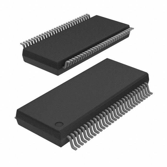
56-Pin 300mil SSOP
* This input has a 50KW pull-down to GND.
Functionality
Block Diagram
X1
X2
XTAL
OSC
/2
FS1
0
0
0
1
X
X
1
0
0
1
1
0
1
0
1
1
1
1
/3
2
PD#
FS0
REF0
PLL1
Spread
Spectrum
FS(2:0)
FS2
3
Control
Logic
Config
Reg
SDATA
13
/2
2
/2
SCLK
PLL2
CPU66/100/133 [1:0]
3V66 (2:0)
SDRAM (12:0)
Function
Tristate
Test
Active CPU = 66MHz
SDRAM = 100MHz
Active CPU = 100MHz
SDRAM = 100MHz
Active CPU = 133MHz
SDRAM = 133MHz
Active CPU = 133MHz
SDRAM = 100MHz
PCICLK (1:0)
IOAPIC
48MHz (1:0)
2
Third party brands and names are the property of their respective owners.
Power Groups
Analog
VDDREF = X1, X2
VDDA = PLL1
VDD48 = PLL2
Digital
VDD3V66, VDDPCI
VDDSDR, VDDL
�ICS9250-28
General Description
The ICS9250-28 is part of a two chip clock solution for 810/810E and 815 type chipset. Combined with the
ICS9112-17, the ICS9250-28 provides all necessary clock signals for such a system.
Spread spectrum may be enabled through I2C programming. Spread spectrum typically reduces EMI by 8dB to 10
dB. This simplifies EMI qualification without resorting to board design iterations or costly shielding. The
ICS9250-28 employs a proprietary closed loop design, which tightly controls the percentage of spreading over
process and temperature variations.
Pin Configuration
PIN NUMBER
P I N NA M E
TYPE
DESCRIPTION
1
IOAPIC
OUT
2.5V clock output running at 33.3MHz.
2, 56
VDDL
PWR
2.5V power supply for CPU & IOAPIC
4
FS1
REF0
5, 9, 14, 20, 25,
VDD
31, 35, 40, 44, 49
IN
Function Select pin. Determines CPU frequency, all output functionality
OUT
3.3V, 14.318MHz reference clock output.
PWR
3.3V power supply
6
X1
IN
7
X2
OUT
Crystal input, has internal load cap (33pF) and feedback
resistor from X2
Crystal output, nominally 14.318MHz. Has internal load
cap (33pF)
GND
PWR
Ground pins for 3.3V supply
3V66 (2:0)
OUT
3 . 3 V F i xe d 6 6 M H z c l o c k o u t p u t s f o r H U B
3, 8, 13, 17, 19,
24, 30, 34, 39,
43, 48, 52, 55
12, 11, 10
28, 18
FS (2, 0)
16, 15
PCICLK[1:0]
IN
OUT
Function Select pins. Determines CPU frequency, all output functionality.
Please refer to Functionality table on page 3.
3.3V PCI clock outputs
21
PD#
IN
Asynchronous active low input pin used to power down the device into
a low power state. The internal clocks are disabled and the VCO and
the crystal are stopped. The latency of the power down will not be
greater than 3ms.
22
SCLK
IN
Clock pin of I2C circuitry 5V tolerant
23
SDATA
I/O
Data pin for I2C circuitry 5V tolerant
26, 27
48MHz_0
29, 32, 33, 36,
AM
37, 38, 41, 42, (S1D2R
:0)
45, 46, 47, 50, 51
54, 53
CPUCLK (1:0)
OUT
3 . 3 V F i xe d 4 8 M H z c l o c k o u t p u t s .
OUT
3.3V output running 100MHz. All SDRAM outputs can be turned off
t h r o u g h I 2C
OUT
2.5V Host bus clock output. 66MHz, 100MHz or 133MHz depending
on FS (2:0) pins.
2
�ICS9250-28
Power Down Waveform
Note
1. After PD# is sampled active (Low) for 2 consective rising edges of CPUCLKs, all
the output clocks are driven Low on their next High to Low tranistiion.
2. Power-up latency