IDT5V995
3.3V PROGRAMMABLE SKEW PLL CLOCK DRIVER TURBOCLOCK II
INDUSTRIAL TEMPERATURE RANGE
3.3V PROGRAMMABLE
SKEW PLL CLOCK DRIVER
TURBOCLOCK™ II
IDT5V995
FEATURES:
DESCRIPTION:
•
•
•
•
The IDT5V995 is a high fanout 3.3V PLL based clock driver intended for
high performance computing and data-communications applications. A key
feature of the programmable skew is the ability of outputs to lead or lag the
REF input signal. The IDT5V995 has eight programmable skew outputs in
four banks of 2. Skew is controlled by 3-level input signals that may be hardwired to appropriate HIGH-MID-LOW levels.
The feedback input allows divide-by-functionality from 1 to 12 through the
use of the DS[1:0] inputs. This provides the user with frequency
multiplication from 1 to 12 without using divided outputs for feedback.
When the sOE pin is held low, all the outputs are synchronously enabled.
However, if sOE is held high, all the outputs except 2Q0 and 2Q1 are
synchronously disabled. The LOCK output asserts to indicate when Phase
Lock has been achieved.
Furthermore, when PE is held high, all the outputs are synchronized with
the positive edge of the REF clock input. When PE is held low, all the outputs
are synchronized with the negative edge of REF. The IDT5V995 has
LVTTL outputs with 12mA balanced drive outputs.
Ref input is 5V tolerant
4 pairs of programmable skew outputs
Low skew: 185ps same pair, 250ps all outputs
Selectable positive or negative edge synchronization:
Excellent for DSP applications
Synchronous output enable
Input frequency: 2MHz to 200MHz
Output frequency: 6MHz to 200MHz
3-level inputs for skew and PLL range control
3-level inputs for feedback divide selection multiply / divide
ratios of (1-6, 8, 10, 12) / (2, 4)
PLL bypass for DC testing
External feedback, internal loop filter
12mA balanced drive outputs
Low Jitter: 3MHz)
tCCJLA
Cycle-to-Cycle Output Jitter (peak-to-peak)
(divide by 1 output frequency, FS = L, FREF < 3MHz)
NOTES:
1. Refer to Input Timing Requirements table for more detail.
2. Skew is the time between the earliest and the latest output transition among all outputs for which the same tU delay has been selected when all are loaded with the specified
load.
3. tSKEWPR is the skew between a pair of outputs (xQ0 and xQ1) when all eight outputs are selected for 0tU.
4. tSK(0) is the skew between outputs when they are selected for 0tU.
5. There are 3 classes of outputs: Nominal (multiple of tU delay), Inverted (4Q0 and 4Q1 only with 4F0 = 4F1 = HIGH), and Divided (3Qx and 4Qx only in Divide-by-2 or Divideby-4 mode). Test condition: nF0:1=MM is set on unused outputs.
6. tDEV is the output-to-output skew between any two devices operating under the same conditions (VDDQ, VDD, ambient temperature, air flow, etc.)
7. tφ is measured with REF input rise and fall times (from 0.8V to 2V) of 0.5ns. Measured from 1.5V on REF to 1.5V on FB.
8. Measured at 2V.
9. Measured at 0.8V.
10. tLOCK is the time that is required before synchronization is achieved. This specification is valid only after VDD/VDDQ is stable and within normal operating limits. This parameter
is measured from the application of a new signal or frequency at REF or FB until tPD is within specified limits.
11. Lock detector may be unreliable for input frequencies less than approximately 4MHz, or for input signals which contain significant jitter.
7
�IDT5V995
3.3V PROGRAMMABLE SKEW PLL CLOCK DRIVER TURBOCLOCK II
INDUSTRIAL TEMPERATURE RANGE
AC TEST LOADS AND WAVEFORMS
V D DQ
150 Ω
Outpu t
Output
150 Ω
20p F
For LOCK output
For all other o utputs
t O FA LL
t OR IS E
t PW H
2.0 V
V TH = 1 .5V
0.8 V
tP W L
LVTTL Output Waveform
≤ 1 ns
3.0V
2.0V
V TH = 1.5V
0.8V
0V
LVTTL Input Test Waveform
8
≤ 1 ns
20pF
�IDT5V995
3.3V PROGRAMMABLE SKEW PLL CLOCK DRIVER TURBOCLOCK II
INDUSTRIAL TEMPERATURE RANGE
AC TIMING DIAGRAM
t RPW L
t REF
tRPW H
REF
t (φ)
tO DC V
tO DCV
FB
t CCJH, HA,
M, L, LA
Q
t SKEW PR
t SKEW 0, 1
tSKEW PR
tSKEW 0, 1
OTHER Q
t SKEW 2
t SKEW 2
INVER TED Q
tSKEW 3, 4
t SKEW 3, 4
tSKEW 3, 4
REF DIVIDED BY 2
tSKEW1, 3, 4
tSKEW 2, 4
REF DIVIDED BY 4
NOTES:
PE:
Skew:
The AC Timing Diagram applies to PE=VDD. For PE=GND, the negative edge of FB aligns with the negative edge of REF, divided outputs change on the negative edge
of REF, and the positive edges of the divide-by-2 and the divide-by-4 signals align.
The time between the earliest and the latest output transition among all outputs for which the same tU delay has been selected when all are loaded with 20pF and terminated
with 75Ω to VDDQ/2.
tSKEWPR:
The skew between a pair of outputs (xQ0 and xQ1) when all eight outputs are selected for 0tU.
tSKEW0:
The skew between outputs when they are selected for 0tU.
tDEV:
The output-to-output skew between any two devices operating under the same conditions (VDDQ, VDD, ambient temperature, air flow, etc.)
tODCV:
The deviation of the output from a 50% duty cycle. Output pulse width variations are included in tSKEW2 and tSKEW4 specifications.
tPWH is measured at 2V.
tPWL is measured at 0.8V.
tORISE and tOFALL are measured between 0.8V and 2V.
tLOCK:
The time that is required before synchronization is achieved. This specification is valid only after VDD/VDDQ is stable and within normal operating limits. This parameter
is measured from the application of a new signal or frequency at REF or FB until tPD is within specified limits.
9
�IDT5V995
3.3V PROGRAMMABLE SKEW PLL CLOCK DRIVER TURBOCLOCK II
INDUSTRIAL TEMPERATURE RANGE
ORDERING INFORMATION
XXXXX
Device Type
XX
Package
X
Package
I
-40°C to +85°C (Industrial)
PF
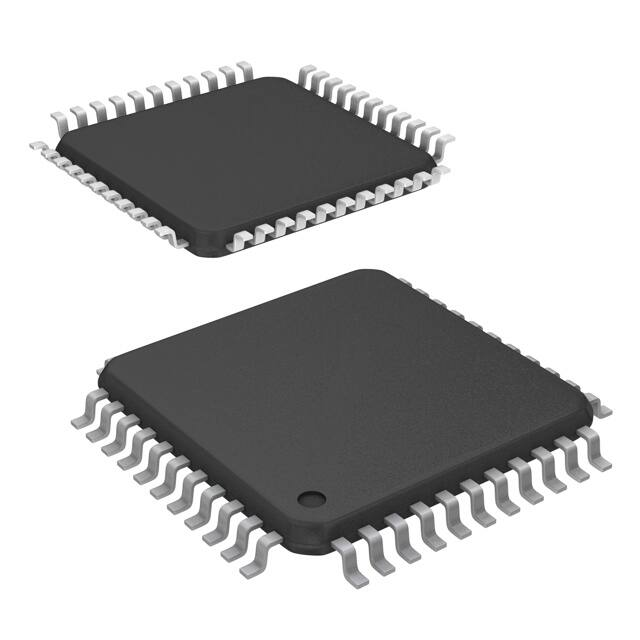
PFG
Thin Quad Flat Pack
TQFP - Green
5V995
3.3V Programmable Skew PLL Clock Driver TurboClock II
CORPORATE HEADQUARTERS
6024 Silver Creek Valley Road
San Jose, CA 95138
for SALES:
800-345-7015 or 408-284-8200
fax: 408-284-2775
www.idt.com
10
for Tech Support:
clockhelp@idt.com
�
很抱歉,暂时无法提供与“IDT5V995PFGI8”相匹配的价格&库存,您可以联系我们找货
免费人工找货