64K x 32
3.3V Synchronous SRAM
Pipelined Outputs
Burst Counter, Single Cycle Deselect
71V632
Features
◆
◆
◆
◆
64K x 32 memory configuration
Supports high system speed:
Commercial and Industrial:
– 5 5ns clock access time (100 MHz)
– 6 6ns clock access time (83 MHz)
– 7 7ns clock access time (66 MHz)
Single-cycle deselect functionality
LBO input selects interleaved or linear burst mode
◆
◆
◆
◆
◆
Self-timed write cycle with global write control (GW), byte
write enable (BWE), and byte writes (BWx)
Power down controlled by ZZ input
Operates with a single 3.3V power supply (+10/-5%)
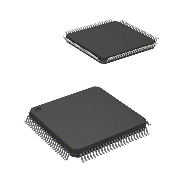
Packaged in a JEDEC Standard 100-pin rectangular plastic
thin quad flatpack (TQFP)
Green parts available, see ordering information
Functional Block Diagram
LBO
ADV
CLK
2
Binary
Counter
ADSC
Burst
Logic
Q0
CLR
ADSP
INTERNAL
ADDRESS
Burst
Sequence
CE
Q1
CLK EN
ADDRESS
REGISTER
A0–A15
GW
BWE
64K x 32
BIT
MEMORY
ARRAY
16
A0*
A1*
.
2
A0, A1
A2–A15
32
32
16
Byte 1
Write Register
Byte 1
Write Driver
BW1
8
Byte 2
Write Register
Byte 2
Write Driver
BW2
8
Byte 3
Write Register
Byte 3
Write Driver
BW3
8
Byte 4
Write Register
Byte 4
Write Driver
BW4
8
OUTPUT
REGISTER
CE
CS0
CS1
D
Q
Enable
Register
DATA INPUT
REGISTER
CLK EN
ZZ
Powerdown
D
Q
Enable
Delay
Register
OE
OE
OUTPUT
BUFFER
32
I/O0–I/O31
3619 drw 01
1
Mar.09.20
�71V632, 64K x 32, 3.3V Synchronous SRAM
with Pipelined Outputs and Single Cycle Deselect
Description
Commercial and Industrial Temperature Ranges
The IDT71V632 is a 3.3V high-speed SRAM organized as 64K x 32
with full support of the Pentium™ and PowerPC™ processor interfaces.
The pipelined burst architecture provides cost-effective 3-1-1-1 secondary cache performance for processors up to 100MHz.
The IDT71V632 SRAM contains write, data, address, and control
registers. Internal logic allows the SRAM to generate a self-timed write
based upon a decision which can be left until the extreme end of the write
cycle.
The burst mode feature offers the highest level of performance to the
system designer, as the IDT71V632 can provide four cycles of data for
a single address presented to the SRAM. An internal burst address counter
accepts the first cycle address from the processor, initiating the access
sequence. The first cycle of output data will be pipelined for one cycle before
it is available on the next rising clock edge. If burst mode operation is
selected (ADV=LOW), the subsequent three cycles of output data will be
available to the user on the next three rising clock edges. The order of these
three addresses will be defined by the internal burst counter and the LBO
input pin.
The IDT71V632 SRAM utilizes a high-performance, high-volume
3.3V CMOS process, and is packaged in a JEDEC Standard 14mm x
20mm 100-pin thin plastic quad flatpack (TQFP) for optimum board density
in both desktop and notebook applications.
Pin Description Summary
A0–A15
Ad d re ss Inp uts
Inp ut
Synchro no us
CE
Chip Enab le
Inp ut
Synchro no us
CS0, CS1
Chip s Se le cts
Inp ut
Synchro no us
OE
Outp ut Enab le
Inp ut
Asynchro no us
GW
Glo b al Write Enab le
Inp ut
Synchro no us
BWE
Byte Write Enab le
Inp ut
Synchro no us
BW1, BW2, BW3, BW4
Ind ivid ual Byte Write Se le cts
Inp ut
Synchro no us
CLK
Clo ck
Inp ut
N/A
ADV
Burst Ad d re ss Ad vance
Inp ut
Synchro no us
ADSC
Ad d re ss Status (Cache Co ntro lle r)
Inp ut
Synchro no us
ADSP
Ad d re ss Status (Pro ce sso r)
Inp ut
Synchro no us
LBO
Line ar / Inte rle ave d Burst Ord e r
Inp ut
DC
ZZ
S le e p Mo d e
Inp ut
Asynchro no us
I/O0–I/O31
Data Inp ut/Outp ut
I/O
Synchro no us
VDD, VDDQ
3.3V
Po we r
N/A
VSS, VSSQ
Array Gro und , I/O Gro und
Po we r
N/A
3619 tb l 01
Pentium processor is a trademark of Intel Corp.
PowerPC is a trademark of International Business Machines, Inc.
6.42
2
Mar.09.20
�71V632, 64K x 32, 3.3V Synchronous SRAM
with Pipelined Outputs and Single Cycle Deselect
Commercial and Industrial Temperature Ranges
Pin Definitions(1)
Symbol
Pin Function
I/O
Active
A0–A15
Description
Ad d re ss Inp uts
I
N/A
Synchro no us Ad d re ss inp uts. The ad d re ss re g iste r is trig g e re d b y a co mb inatio n
o f the rising e d g e o f CLK and ADSC Lo w o r ADSP Lo w and CE Lo w.
ADSC
Ad d re ss Status
(Cache Co ntro lle r)
I
LOW
Synchro no us Ad d re ss Status fro m Cache Co ntro lle r.ADSC is an active LOW
inp ut that is use d to lo ad the ad d re ss re g iste rs with ne w ad d re sse s. ADSC is
NOT GATED b y CE.
ADSP
Ad d re ss Status
(Pro ce sso r)
I
LOW
ADV
Burst Ad d re ss Ad vance
I
LOW
Synchro no us Ad d re ss Ad vance . ADV is an active LOW inp ut that is use d to
ad vance the inte rnal b urst co unte r, co ntro lling b urst acce ss afte r the initial
ad d re ss is lo ad e d . Whe n this inp ut is HIGH the b urst co unte r is no t incre me nte d ;
that is, the re is no ad d re ss ad vance .
BWE
Byte Write Enab le
I
LOW
Synchro no us b yte write e nab le g ate s the b yte write inp uts BW1–BW4. If BWE is
LOW at the rising e d g e o f CLK the n BWX inp uts are p asse d to the ne xt stag e in
the circuit. A b yte write can still b e b lo cke d if ADSP is LOW at the rising e d g e o f
CLK. If ADSP is HIGH and BWX is LOW at the rising e d g e o f CLK the n d ata will
b e writte n to the SRAM. If BWE is HIGH the n the b yte write inp uts are b lo cke d
and o nly GW can initiate a write cycle .
BW1–BW4
Ind ivid ual Byte
Write Enab le s
I
LOW
Synchro no us b yte write e nab le s. BW1 co ntro ls I/O(7:0), BW2 co ntro ls I/O(15:8),
e tc. Any active b yte write cause s all o utp uts to b e d isab le d . ADSP LOW
d isab le s all b yte write s. BW1–BW4 must me e t sp e cifie d se tup and ho ld time s
with re sp e ct to CLK.
CE
Chip Enab le
I
LOW
Synchro no us chip e nab le . CE is use d with CS0 and CS1 to e nab le the
IDT71V632. CE also g ate s ADSP.
CLK
Clo ck
I
N/A
This is the clo ck inp ut. All timing re fe re nce s fo r the d e vice are mad e with re sp e ct
to this inp ut.
CS0
Chip Se le ct 0
I
HIGH
Synchro no us active HIGH chip se le ct. CS0 is use d with CE and CS1 to e nab le
the chip .
CS1
Chip Se le ct 1
I
LOW
Synchro no us active LOW chip se le ct. CS1 is use d with CE and CS0 to e nab le
the chip .
GW
Glo b al Write Enab le
I
LOW
I/O0–I/O31
Data Inp ut/Outp ut
I/O
N/A
Synchro no us d ata inp ut/o utp ut (I/O) p ins. Bo th the d ata inp ut p ath and d ata o utp ut
p ath are re g iste re d and trig g e re d b y the rising e d g e o f CLK.
LBO
Line ar Burst Ord e r
I
LOW
Asynchro no us b urst o rd e r se le ctio n DC inp ut. Whe n LBO is HIGH the Inte rle ave d
(Inte l) b urst se q ue nce is se le cte d . Whe n LBO is LOW the Line ar (Po we rPC) b urst
se q ue nce is se le cte d . LBO is a static DC inp ut and must no t chang e state while
the d e vice is o p e rating .
OE
Outp ut Enab le
I
LOW
Asynchro no us o utp ut e nab le . Whe n OE is LOW the d ata o utp ut d rive rs are
e nab le d o n the I/O p ins if the chip is also se le cte d . Whe n OE is HIGH the I/O
p ins are in a hig h-imp e d e nce state .
VDD
Po we r Sup p ly
N/A
N/A
3.3V co re p o we r sup p ly inp uts.
VDDQ
Po we r Sup p ly
N/A
N/A
3.3V I/O p o we r sup p ly inp uts.
VSS
Gro und
N/A
N/A
Co re g ro und p ins.
VSSQ
Gro und
N/A
N/A
I/O g ro und p ins.
NC
No Co nne ct
N/A
N/A
NC p ins are no t e le ctrically co nne cte d to the chip .
ZZ
S le e p Mo d e
I
HIGH
Asynchro no us sle e p mo d e inp ut. ZZ HIGH will g ate the CLK inte rnally and p o we r
d o wn the IDT71V632 to its lo we st p o we r co nsump tio n le ve l. Data re te ntio n is
g uarante e d in Sle e p Mo d e .
Synchro no us Ad d re ss Status fro m Pro ce sso r. ADSP is an active LOW inp ut that
is use d to lo ad the ad d re ss re g iste rs with ne w ad d re sse s. ADSP is g ate d b y
CE.
Synchro no us g lo b al write e nab le . This inp ut will write all fo ur 8-b it d ata b yte s
whe n LOW o n the rising e d g e o f CLK. GW sup e rce d e s ind ivid ual b yte write
e nab le s.
NOTE:
1. All synchronous inputs must meet specified setup and hold times with respect to CLK.
6.42
3
Mar.09.20
3619 tb l 02
�71V632, 64K x 32, 3.3V Synchronous SRAM
with Pipelined Outputs and Single Cycle Deselect
Commercial and Industrial Temperature Ranges
Absolute Maximum Ratings(1)
Symbol
Rating
Value
Unit
VTERM(2)
Te rminal Vo ltag e with
Re sp e ct to GND
–0.5 to +4.6
V
VTERM(3)
Te rminal Vo ltag e with
Re sp e ct to GND
–0.5 to VDD+0.5
V
TA
Op e rating Te mp e rature
0 to +70
o
C
TBIAS
Te mp e rature Und e r Bias
–55 to +125
o
C
–55 to +125
o
C
TSTG
Sto rag e Te mp e rature
PT
Po we r Dissip atio n
1.0
IOUT
DC Outp ut Curre nt
50
Recommended Operating
Temperature and Supply Voltage
Grade
Temperature
VSS
VDD
VDDQ
Co mme rcial
0° C to +70° C
0V
3.3V+10/-5% 3.3V+10/-5%
Ind ustrial
–40° C to +85° C
0V
3.3V+10/-5% 3.3V+10/-5%
3619 tb l 03
Recommended DC Operating
Conditions
W
mA
3619 tb l 05
NOTES:
1. Stresses greater than those listed under ABSOLUTE MAXIMUM RATINGS may
cause permanent damage to the device. This is a stress rating only and functional
operation of the device at these or any other conditions above those indicated
in the operational sections of this specification is not implied. Exposure to absolute
maximum rating conditions for extended periods may affect reliability.
2. VDD, VDDQ and Input terminals only.
3. I/O terminals.
Symbol
Parameter
M i n.
Max.
Unit
VDD
Co re Sup p ly Vo ltag e
3.135
3.63
V
VDDQ
I/O Sup p ly Vo ltag e
3.135
3.63
V
VSS, VSSQ
Gro und
0
0
V
VIH
VIH
VIL
Inp ut Hig h Vo ltag e — Inp uts
Inp ut Hig h Vo ltag e — I/O
Inp ut Lo w Vo ltag e
2.0
2.0
(3)
–0.3
(1)
5.0
V
(2)
VDDQ+0.3
0.8
V
V
3619 tb l 04
NOTES:
1. VIH (max) = 6.0V for pulse width less than tCYC/2, once per cycle.
2. VIH (max) = VDDQ + 1.0V for pulse width less than tCYC/2, once per cycle.
3. VIL (min) = –1.0V for pulse width less than tCYC/2, once per cycle.
Capacitance
(TA = +25°C, f = 1.0MHz, TQFP package)
Parameter(1)
Symbol
CIN
Inp ut Cap acitance
CI/O
I/O Cap acitance
Conditions
Max.
Unit
VIN = 3d V
6
pF
VOUT = 3d V
7
pF
3619 tb l 06
NOTE:
1. This parameter is guaranteed by device characterization, but not production
tested.
6.42
4
Mar.09.20
�71V632, 64K x 32, 3.3V Synchronous SRAM
with Pipelined Outputs and Single Cycle Deselect
Commercial and Industrial Temperature Ranges
A6
A7
CE
CS0
BW4
BW3
BW2
BW1
CS1
VDD
VSS
CLK
GW
BWE
OE
ADSC
ADSP
ADV
A8
A9
Pin Configuration
100 99 98 97 96 95 94 93 92 91 90 89 88 87 86 85 84 83 82 81
NC
I/O16
I/O17
VDDQ
VSSQ
I/O18
I/O19
I/O20
I/O21
VSSQ
VDDQ
I/O22
I/O23
VDD/NC(1)
VDD
NC
VSS
I/O24
I/O25
VDDQ
VSSQ
I/O26
I/O27
I/O28
I/O29
VSSQ
VDDQ
I/O30
I/O31
NC
1
80
2
79
3
78
4
77
5
6
76
75
7
74
8
73
9
72
71
10
11
12
13
71V632
PKG100
70
69
68
14
67
15
66
16
65
64
17
18
19
63
62
20
61
21
60
22
59
23
24
58
57
25
56
26
55
27
54
28
53
29
52
30
51
NC
I/O15
I/O14
VDDQ
VSSQ
I/O13
I/O12
I/O11
I/O10
VSSQ
VDDQ
I/O9
I/O8
VSS
NC
VDD
ZZ(2)
I/O7
I/O6
VDDQ
VSSQ
I/O5
I/O4
I/O3
I/O2
VSSQ
VDDQ
I/O1
I/O0
NC
NC
NC
A10
A11
A12
A13
A14
A15
NC
LBO
A5
A4
A3
A2
A1
A0
NC
NC
VSS
VDD
31 32 33 34 35 36 37 38 39 40 41 42 43 44 45 46 47 48 49 50
Top View TQFP
NOTES:
1. Pin 14 can either be directly connected to VDD or not connected.
2. Pin 64 can be left unconnected and the device will always remain in active mode.
6.42
5
Mar.09.20
3619 drw 02
�71V632, 64K x 32, 3.3V Synchronous SRAM
with Pipelined Outputs and Single Cycle Deselect
Commercial and Industrial Temperature Ranges
Synchronous Truth Table(1,2)
Address
Used
CE
CS0
CS1
ADSP
ADSC
ADV
GW
BWE
BWX
OE(3)
CLK
I/O
De se le cte d Cycle , Po we r Do wn
No ne
H
X
X
X
L
X
X
X
X
X
↑
Hi-Z
De se le cte d Cycle , Po we r Do wn
No ne
L
X
H
L
X
X
X
X
X
X
↑
Hi-Z
De se le cte d Cycle , Po we r Do wn
No ne
L
L
X
L
X
X
X
X
X
X
↑
Hi-Z
De se le cte d Cycle , Po we r Do wn
No ne
L
X
H
X
L
X
X
X
X
X
↑
Hi-Z
De se le cte d Cycle , Po we r Do wn
No ne
L
L
X
X
L
X
X
X
X
X
↑
Hi-Z
Re ad Cycle , Be g in Burst
Exte rnal
L
H
L
L
X
X
X
X
X
L
↑
DOUT
Re ad Cycle , Be g in Burst
Exte rnal
L
H
L
L
X
X
X
X
X
H
↑
Hi-Z
Re ad Cycle , Be g in Burst
Exte rnal
L
H
L
H
L
X
H
H
X
L
↑
DOUT
Re ad Cycle , Be g in Burst
Exte rnal
L
H
L
H
L
X
H
L
H
L
↑
DOUT
Re ad Cycle , Be g in Burst
Exte rnal
L
H
L
H
L
X
H
L
H
H
↑
Hi-Z
Write Cycle , Be g in Burst
Exte rnal
L
H
L
H
L
X
H
L
L
X
↑
DIN
Write Cycle , Be g in Burst
Exte rnal
L
H
L
H
L
X
L
X
X
X
↑
DIN
Re ad Cycle , Co ntinue Burst
Ne xt
X
X
X
H
H
L
H
H
X
L
↑
DOUT
Re ad Cycle , Co ntinue Burst
Ne xt
X
X
X
H
H
L
H
H
X
H
↑
Hi-Z
Re ad Cycle , Co ntinue Burst
Ne xt
X
X
X
H
H
L
H
X
H
L
↑
DOUT
Re ad Cycle , Co ntinue Burst
Ne xt
X
X
X
H
H
L
H
X
H
H
↑
Hi-Z
Re ad Cycle , Co ntinue Burst
Ne xt
H
X
X
X
H
L
H
H
X
L
↑
DOUT
Re ad Cycle , Co ntinue Burst
Ne xt
H
X
X
X
H
L
H
H
X
H
↑
Hi-Z
Re ad Cycle , Co ntinue Burst
Ne xt
H
X
X
X
H
L
H
X
H
L
↑
DOUT
Re ad Cycle , Co ntinue Burst
Ne xt
H
X
X
X
H
L
H
X
H
H
↑
Hi-Z
Write Cycle , Co ntinue Burst
Ne xt
X
X
X
H
H
L
H
L
L
X
↑
DIN
Write Cycle , Co ntinue Burst
Ne xt
X
X
X
H
H
L
L
X
X
X
↑
DIN
Write Cycle , Co ntinue Burst
Ne xt
H
X
X
X
H
L
H
L
L
X
↑
DIN
Write Cycle , Co ntinue Burst
Ne xt
H
X
X
X
H
L
L
X
X
X
↑
DIN
Re ad Cycle , Susp e nd Burst
Curre nt
X
X
X
H
H
H
H
H
X
L
↑
DOUT
Re ad Cycle , Susp e nd Burst
Curre nt
X
X
X
H
H
H
H
H
X
H
↑
Hi-Z
Re ad Cycle , Susp e nd Burst
Curre nt
X
X
X
H
H
H
H
X
H
L
↑
DOUT
Re ad Cycle , Susp e nd Burst
Curre nt
X
X
X
H
H
H
H
X
H
H
↑
Hi-Z
Re ad Cycle , Susp e nd Burst
Curre nt
H
X
X
X
H
H
H
H
X
L
↑
DOUT
Re ad Cycle , Susp e nd Burst
Curre nt
H
X
X
X
H
H
H
H
X
H
↑
Hi-Z
Re ad Cycle , Susp e nd Burst
Curre nt
H
X
X
X
H
H
H
X
H
L
↑
DOUT
Re ad Cycle , Susp e nd Burst
Curre nt
H
X
X
X
H
H
H
X
H
H
↑
Hi-Z
Write Cycle , Susp e nd Burst
Curre nt
X
X
X
H
H
H
H
L
L
X
↑
DIN
Write Cycle , Susp e nd Burst
Curre nt
X
X
X
H
H
H
L
X
X
X
↑
DIN
Write Cycle , Susp e nd Burst
Curre nt
H
X
X
X
H
H
H
L
L
X
↑
DIN
Write Cycle , Susp e nd Burst
Curre nt
H
X
X
X
H
H
L
X
X
X
↑
DIN
Operation
NOTES:
1. L = VIL, H = VIH, X = Don’t Care.
2. ZZ = LOW for this table.
3. OE is an asynchronous input.
3619 tb l 07
6.42
6
Mar.09.20
�71V632, 64K x 32, 3.3V Synchronous SRAM
with Pipelined Outputs and Single Cycle Deselect
Commercial and Industrial Temperature Ranges
Synchronous Write Function Truth Table(1)
GW
BWE
BW1
BW2
BW3
BW4
Re ad
H
H
X
X
X
X
Re ad
H
L
H
H
H
H
Write all Byte s
L
X
X
X
X
X
Write all Byte s
H
L
L
L
L
L
Write Byte 1(2)
H
L
L
H
H
H
Write Byte 2(2)
H
L
H
L
H
H
(2)
H
L
H
H
L
H
(2)
H
L
H
H
H
L
Operation
Write Byte 3
Write Byte 4
NOTES:
1. L = VIL, H = VIH, X = Don’t Care.
2. Multiple bytes may be selected during the same cycle.
3619 tb l 08
Asynchronous Truth Table(1)
OE
ZZ
I/O Status
Power
Re ad
L
L
Data Out (I/O0 - I/O31)
Active
Re ad
H
L
Hig h-Z
Active
Write
X
L
Hig h-Z — Data In (I/O0 - I/O31)
Active
De se le cte d
X
L
Hig h-Z
Stand b y
S le e p
X
H
Hig h-Z
S le e p
Operation(2)
NOTES:
1. L = VIL, H = VIH, X = Don’t Care.
2. Synchronous function pins must be biased appropriately to satisfy operation requirements.
3619 tb l 09
Interleaved Burst Sequence Table (LBO=VDD)
Sequence 1
Sequence 2
Sequence 3
Sequence 4
A1
A0
A1
A0
A1
A0
A1
A0
First Ad d re ss
0
0
0
1
1
0
1
1
Se co nd Ad d re ss
0
1
0
0
1
1
1
0
Third Ad d re ss
1
0
1
1
0
0
0
1
Fo urth Ad d re ss(1)
1
1
1
0
0
1
0
0
NOTE:
1. Upon completion of the Burst sequence the counter wraps around to its initial state.
3619 tb l 10
Linear Burst Sequence Table (LBO=VSS)
Sequence 1
Sequence 2
Sequence 3
A1
A0
A1
A0
A1
A0
A1
A0
First Ad d re ss
0
0
0
1
1
0
1
1
Se co nd Ad d re ss
0
1
1
0
1
1
0
0
Third Ad d re ss
1
0
1
1
0
0
0
1
1
1
0
0
0
1
1
0
Fo urth Ad d re ss
(1)
NOTE:
1. Upon completion of the Burst sequence the counter wraps around to its initial state.
6.42
7
Mar.09.20
Sequence 4
3619 tb l 11
�71V632, 64K x 32, 3.3V Synchronous SRAM
with Pipelined Outputs and Single Cycle Deselect
Commercial and Industrial Temperature Ranges
DC Electrical Characteristics Over the Operating Temperature and
Supply Voltage Range (VDD = 3.3V +10/-5%)
Symbol
Parameter
Test Conditions
Min.
Max.
Unit
VDD = Max., VIN = 0V to VDD
—
5
µA
|ILI|
Inp ut Le akag e Curre nt
|ILZZ|
ZZ and LBO Inp ut Le akag e Curre nt
VDD = Max., VIN = 0V to VDD
—
30
µA
|ILO|
Outp ut Le akag e Curre nt
CE > VIH o r OE > VIH, VOUT = 0V to VDD, VDD = Max.
—
5
µA
VOL (3.3V)
Outp ut Lo w Vo ltag e
IOL = 5mA, VDD = Min.
—
0.4
V
VOH (3.3V)
Outp ut Hig h Vo ltag e
IOH = –5mA, VDD = Min.
2.4
—
V
(1)
3619 tb l 12
NOTE:
1. The LBO pin will be internally pulled to VDD if it is not actively driven in the application and the ZZ pin will be internally pulled to VSS if not actively driven.
DC Electrical Characteristics Over the Operating Temperature and
Supply Voltage Range(1) (VHD = VDDQ – 0.2V, VLD = 0.2V)
SA4(3,4)
Symbol
Parameter
Test Conditions
S5
S6
S7
Com'l.
Ind.
Com'l.
Ind.
Com'l.
Ind.
Com'l.
Ind.
Unit
IDD
Op e rating Po we r
Sup p ly Curre nt
De vice Se le cte d , Outp uts Op e n,
VDD = Max., VIN > VIH o r < VIL,
f = fMAX(2)
220
—
200
200
180
180
160
160
mA
ISB
Stand b y Po we r
Sup p ly Curre nt
De vice De se le cte d , Outp uts Op e n,
VDD = Max., VIN > VIH o r < VIL,
f = fMAX(2)
70
—
65
65
60
60
55
55
mA
ISB1
Full Stand b y Po we r
Sup p ly Curre nt
De vice De se le cte d , Outp uts Op e n,
VDD = Max., VIN > VHD o r < VLD,
f = 0(2)
15
—
15
15
15
15
15
15
mA
IZZ
Full Sle e p Mo d e
ZZ > VHD, VDD = Max.
Po we r Sup p ly Curre nt
10
—
10
10
10
10
10
10
mA
NOTES:
1. All values are maximum guaranteed values.
2. At f = fMAX, inputs are cycling at the maximum frequency of read cycles of 1/tCYC while ADSC = LOW; f=0 means no input lines are changing.
3. SA4 speed grade corresponds to a tCD of 4.5 ns.
4. 0°C to +70°C temperature range only.
+3.3V
AC Test Loads
317Ω
VDDQ/2
I/O
50Ω
I/O
3619 tb l 13
351Ω
5pF*
Z0 = 50Ω
Figure 1. AC Test Load
3619 drw 04
3619 drw 03
6
* Including scope and jig capacitance.
5
Figure 2. High-Impedance Test Load
(for tOHZ, tCHZ, tOLZ, and tDC1)
4
AC Test Conditions
3
ΔtCD
(Typical, ns)
2
Inp ut Pulse Le ve ls
1
20 30 50
80 100
Capacitance (pF)
200
3619 drw 05
Inp ut Rise /Fall Time s
2ns
Inp ut Timing Re fe re nce Le ve ls
1.5V
Outp ut Timing Re fe re nce Le ve ls
1.5V
AC Te st Lo ad
Figure 3. Lumped Capacitive Load, Typical Derating
0 to 3.0V
Se e Fig ure s 1 and 2
3619 tb l 14
6.42
8
Mar.09.20
�71V632, 64K x 32, 3.3V Synchronous SRAM
with Pipelined Outputs and Single Cycle Deselect
Commercial and Industrial Temperature Ranges
AC Electrical Characteristics
(VDD, VDDQ = 3.3V +10/-5%, Commercial and Industrial Temperature Ranges)
71V632SA4(5,6)
Symbol
Parameter
71V632S5
71V632S6
71V632S7
Min.
Max.
Min.
Max.
Min.
Max.
Min.
Max.
Unit
CLOCK PARAMETERS
tCYC
Clo ck Cycle Time
8.5
____
10
____
12
____
15
____
ns
tCH(1)
Clo ck Hig h Pulse Wid th
3.5
____
4
____
4.5
____
5
____
ns
tCL(1)
Clo ck Lo w Pulse Wid th
3.5
____
4
____
4.5
____
5
____
ns
____
4.5
____
5
____
6
____
7
ns
1.5
____
2
____
2
____
ns
0
____
0
____
0
____
ns
OUTPUT PARAMETERS
tCD
Clo ck Hig h to Valid Data
tCDC
Clo ck Hig h to Data Chang e
1.5
____
tCLZ(2)
Clo ck Hig h to Outp ut Active
0
____
tCHZ(2)
Clo ck Hig h to Data Hig h-Z
1.5
4
1.5
5
2
5
2
6
ns
Outp ut Enab le Acce ss Time
____
4
____
5
____
5
____
6
ns
0
____
0
____
0
____
0
____
ns
Outp ut Enab le Hig h to Data Hig h-Z
____
4
____
4
____
5
____
6
ns
Ad d re ss Se tup Time
2.2
____
2.5
____
2.5
____
2.5
____
ns
2.2
____
2.5
____
2.5
____
2.5
____
ns
2.2
____
2.5
____
2.5
____
2.5
____
ns
2.5
____
2.5
____
2.5
____
ns
tOE
(2)
tOLZ
(2)
tOHZ
Outp ut Enab le Lo w to Data Active
SETUP TIMES
tSA
tSS
Ad d re ss Status Se tup Time
tSD
Data in Se tup Time
tSW
Write Se tup Time
2.2
____
tSAV
Ad d re ss Ad vance Se tup Time
2.2
____
2.5
____
2.5
____
2.5
____
ns
tSC
Chip Enab le /Se le ct Se tup Time
2.2
____
2.5
____
2.5
____
2.5
____
ns
Ad d re ss Ho ld Time
0.5
____
0.5
____
0.5
____
0.5
____
ns
0.5
____
0.5
____
0.5
____
ns
HOLD TIMES
tHA
tHS
Ad d re ss Status Ho ld Time
0.5
____
tHD
Data In Ho ld Time
0.5
____
0.5
____
0.5
____
0.5
____
ns
tHW
Write Ho ld Time
0.5
____
0.5
____
0.5
____
0.5
____
ns
0.5
____
0.5
____
0.5
____
0.5
____
ns
0.5
____
0.5
____
0.5
____
0.5
____
ns
tHAV
Ad d re ss Ad vance Ho ld Time
tHC
Chip Enab le /Se le ct Ho ld Time
SLEEP MODE AND CONFIGURATION PARAMETERS
tZZPW
ZZ Pulse Wid th
100
____
100
—
100
____
100
____
ns
tZZR(3)
ZZ Re co ve ry Time
100
____
100
—
100
____
100
____
ns
34
____
50
____
50
____
ns
(4)
tCFG
Co nfig uratio n Se t-up Time
40
—
NOTES:
1. Measured as HIGH above 2.0V and LOW below 0.8V.
2. Transition is measured ±200mV from steady-state.
3. Device must be deselected when powered-up from sleep mode.
4. tCFG is the minimum time required to configure the device based on the LBO input. LBO is a static input and must not change during normal operation.
5. The 71V632SA4 speed grade corresponds to a tCD of 4.5ns.
6. 0°C to +70°C temperature range only.
6.42
9
Mar.09.20
3619 tb l 15
�Mar.09.20
6.42
10
Output
Disabled
tSC
tSA
tSS
tHS
Ax
Pipelined
Read
tOLZ
tOE
tHC
tHA
O1(Ax)
Ay
(1)
tCH
tCLZ
tOHZ
tCD
tSW
tCL
O1(Ay)
tCDC
tSAV
tHAV
O2(Ay)
tHW
Burst Pipelined Read
O3(Ay)
O4(Ay)
(Burst wraps around
to its initial state)
A DV inserts a wait-state
O1(Ay)
tCHZ
O2(Ay)
3619 drw 06
NOTES:
1. O1 (Ax) represents the first output from the external address Ax. O1 (Ay) represents the first output from the external address Ay; O2 (Ay) represents the next output data in the burst sequence of the base
address Ay, etc. where A0 and A1 are advancing for the four word burst in the sequence defined by the state of the LBO input.
2. ZZ input is LOW and LBO is Don’t Care for this cycle.
3. CS0 timing transitions are identical but inverted to the CE and CS1 signals. For example, when CE and CS1 are LOW on this waveform, CS0 is HIGH.
DATAOUT
OE
A DV
(Note 3)
C E, C S1
GW , BW E, BW x
ADDRESS
A DSC
A DSP
CLK
tCYC
71V632, 64K x 32, 3.3V Synchronous SRAM
with Pipelined Outputs and Single Cycle Deselect
Commercial and Industrial Temperature Ranges
Timing Waveform of Pipelined Read Cycle(1,2)
�Mar.09.20
6.42
11
tSA
tHA
tSS
tHS
tCLZ
tCD
Single Read
Ax
(2)
tOE
O1(Ax)
tOHZ
tSW
Ay
tCH
Pipelined
Write
I1(Ay)
tSD tHD
tCL
tHW
Az
tOLZ
tCDC
O2(Az)
Pipelined Burst Read
O1(Az)
3619 drw 07
O3(Az)
NOTES:
1. Device is selected through entire cycle; CE and CS1 are LOW, CS0 is HIGH.
2. ZZ input is LOW and LBO is Don’t Care for this cycle.
3. O1(Ax) represents the first output from the external address Ax. I1 (Ay) represents the first input from the external address Ay. O1(Az) represents the first output from the external addresses Az; O2(Az)
represents the next output data in the burst sequence of the base address Az, etc. where A0 and A1 are advancing for the four word burst in the sequence defined by the state of the LBO input.
DATAOUT
DATAIN
OE
ADV
GW
ADDRESS
ADSP
CLK
tCYC
71V632, 64K x 32, 3.3V Synchronous SRAM
with Pipelined Outputs and Single Cycle Deselect
Commercial and Industrial Temperature Ranges
Timing Waveform of Combined Pipelined Read and Write Cycles(1,2,3)
�Mar.09.20
6.42
12
tHC
O4(Aw)
Ax
Burst Read
O3(Aw)
tSC
tSA
tHA
tSS
tHS
Ay
tCL
Single
Write
tOHZ
I1(Ax)
I1(Ay)
BWE is ignored when ADSP initiates burst
tCH
tCYC
I2(Ay)
Burst Write
I2(Ay)
(ADV suspends burst)
tSAV
.
I3(Ay)
tHAV
I4(Ay)
tSD
I1(Az)
tHW
tSW
Az
I3(Az)
3104 drw 08
Burst Write
I2(Az)
tHD
NOTES:
1. ZZ input is LOW, BWE is HIGH, and LBO is Don’t Care for this cycle.
2. O4(Aw) represents the final output data in the burst sequence of the base address Aw. I1(Ax) represents the first input from the external address Ax. I1(Ay) represents the first input from the external address
Ay; I2(Ay) represents the next input data in the burst sequence of the base address Ay, etc. where A0 and A1 are advancing for the four word burst in the sequence defined by the state of the LBO input.
In the case of input I2(Ay) this data is valid for two cycles because ADV is high and has suspended the burst.
3. CS0 timing transitions are identical but inverted to the CE and CS1 signals. For example, when CE and CS1 are LOW on this waveform, CS0 is HIGH.
DATAOUT
DATAIN
OE
ADV
(Note 3)
CE, CS1
GW
ADDRESS
ADSC
ADSP
CLK
71V632, 64K x 32, 3.3V Synchronous SRAM
with Pipelined Outputs and Single Cycle Deselect
Commercial and Industrial Temperature Ranges
Timing Waveform of Write Cycle No. 1 — GW Controlled(1,2,3)
�Mar.09.20
6.42
13
tHC
Burst
Read
O3(Aw)
tSC
tSA
tHA
tSS
tHS
O4(Aw)
Ax
Ay
tCL
Single
Write
tOHZ
I1(Ax)
I1(Ay)
BWx is ignored when ADSP initiates burst
BWE is ignored when ADSP initiates burst
tCH
Burst Write
I2(Ay)
(ADV suspends burst)
I2(Ay)
I3(Ay)
I4(Ay)
tSD
Extended
Burst Write
I1(Az)
tSAV
tHW
tSW
tHW
tSW
Az
I2(Az)
tHD
3104 drw 09
I3(Az)
NOTES:
1. ZZ input is LOW, GW is HIGH, and LBO is Don’t Care for this cycle.
2. O4(Aw) represents the final output data in the burst sequence of the base address Aw. I1(Ax) represents the first input from the external address Ax. I1(Ay) represents the first input from the external address
Ay; I2(Ay) represents the next input data in the burst sequence of the base address Ay, etc. where A0 and A1 are advancing for the four word burst in the sequence defined by the state of the LBO input.
In the case of input I2(Ay) this data is valid for two cycles because ADV is high and has suspended the burst.
3. CS0 timing transitions are identical but inverted to the CE and CS1 signals. For example, when CE and CS1 are LOW on this waveform, CS0 is HIGH.
DATAOUT
DATAIN
OE
ADV
(Note 3)
CE, CS1
BWx
BWE
ADDRESS
ADSC
ADSP
CLK
tCYC
71V632, 64K x 32, 3.3V Synchronous SRAM
with Pipelined Outputs and Single Cycle Deselect
Commercial and Industrial Temperature Ranges
Timing Waveform of Write Cycle No. 2 — Byte Controlled(1,2,3)
�Mar.09.20
6.42
14
tSS
tSC
tSA
tHS
Ax
Single Read
tOLZ
tOE
tHC
tHA
O1(Ax)
tCH
tCL
t ZZPW
Snooze Mode
t ZZR
NOTES:
1. Device must power up in deselected Mode.
2. LBO input is Don’t Care for this cycle.
3. It is not necessary to retain the state of the input registers throughout the Power-down cycle.
4. CS0 timing transitions are identical but inverted to the CE and CS1 signals. For example, when CE and CS1 are LOW on this waveform, CS0 is HIGH.
ZZ
DATAOUT
OE
ADV
(Note 4)
CE, CS1
GW
ADDRESS
ADS
C
ADSP
CLK
tCYC
Az
3104 drw 10
71V632, 64K x 32, 3.3V Synchronous SRAM
with Pipelined Outputs and Single Cycle Deselect
Commercial and Industrial Temperature Ranges
Timing Waveform of Sleep (ZZ) and Power-Down Modes(1,2,3)
�71V632, 64K x 32, 3.3V Synchronous SRAM
with Pipelined Outputs and Single Cycle Deselect
Commercial and Industrial Temperature Ranges
Non-Burst Read Cycle Timing Waveform
CLK
ADSP
ADSC
ADDRESS
Av
Aw
Ax
Ay
Az
GW, BWE, BWx
CE, CS1
CS0
OE
DATAOUT
(Av)
(Aw)
(Ax)
(Ay)
3619 drw 11
NOTES:
1. ZZ input is LOW, ADV is HIGH and LBO is Don’t Care for this cycle.
2. (AX) represents the data for address AX, etc.
3. For read cycles, ADSP and ADSC function identically and are therefore interchangeable.
6.42
15
Mar.09.20
,
�71V632, 64K x 32, 3.3V Synchronous SRAM
with Pipelined Outputs and Single Cycle Deselect
Commercial and Industrial Temperature Ranges
Non-Burst Write Cycle Timing Waveform
CLK
ADSP
ADSC
ADDRESS
Av
Aw
Ax
Ay
Az
(Ax)
(Ay)
(Az)
GW
CE, CS1
CS0
DATAIN
(Av)
(Aw)
,
3619 drw 12
NOTES:
1. ZZ input is LOW, ADV and OE are HIGH, and LBO is Don’t Care for this cycle.
2. (AX) represents the data for address AX, etc.
3. Although only GW writes are shown, the functionality of BWE and BWx together is the same as GW.
4. For write cycles, ADSP and ADSC have different limitations.
6.42
16
Mar.09.20
�71V632, 64K x 32, 3.3V Synchronous SRAM
with Pipelined Outputs and Single Cycle Deselect
Commercial and Industrial Temperature Ranges
Ordering Information
XXXX
S
X
XX
Device
Type
Power
Speed
Package
X
X
X
Process/
Temperature
Range
Blank
8
Tray
Tape and Reel
Blank
I(1)
Commercial (0°C to +70°C)
Industrial (-40°C to +85°C)
G
Green
PF
100-Pin TQFP (PKG100)
5
6
7
Synchronous Access Time in Nanoseconds
71V632
64K x 32 Pipelined Burst Synchronous SRAM
3619 drw 13
NOTES:
1. Contact your local sales office for industrial temp range for other speeds, packages and powers.
Part Number
Speed in Megahertz
tCD Parameter
Clock Cycle Time
71V632S5PF
100 MHz
5 ns
10 ns
71V632S6PF
83 MHz
6 ns
12 ns
71V632S7PF
66 MHz
7 ns
15 ns
3619 tbl 16
Orderable Part Information
Speed
(ns)
5
6
7
Pkg.
Code
Pkg.
Type
Temp.
Grade
71V632S5PFGI
PKG100
TQFP
I
71V632S5PFGI8
PKG100
TQFP
I
Orderable Part ID
71V632S6PFGI
PKG100
TQFP
I
71V632S6PFGI8
PKG100
TQFP
I
71V632S7PFG
PKG100
TQFP
C
71V632S7PFG8
PKG100
TQFP
C
71V632S7PFGI
PKG100
TQFP
I
71V632S7PFGI8
PKG100
TQFP
I
6.42
17
Mar.09.20
,
�71V632, 64K x 32, 3.3V Synchronous SRAM
with Pipelined Outputs and Single Cycle Deselect
Commercial and Industrial Temperature Ranges
Datasheet Document History
09/09/99
09/30/99
04/04/00
08/09/00
08/17/01
02/28/07
10/16/08
05/27/10
02/24/17
Pg. 1, 8, 9, 17
Pg. 15, 16
Pg. 18
Pg. 1, 4, 8, 9, 17
Pg. 17
Pg. 18
Pg. 18
Pg. 17
Pg. 1
Pg. 5
Pg. 14
Pg. 16
Pg. 17
03/09/20
Pg. 1 - 19
Pg. 1 - 2
Pg. 1 & 17
Pg. 17
Updated to new format
Revised speed offerings to 66–117MHz
Added non-burst read and write cycle timing diagrams
Added Datasheet Document History
Added industrial temperature range offerings
Added 100pinTQFP package Diagram Outline
Not recommended for new designs
Removed “Not recommended for new designs” from the background on the datasheet
Added Z generation die step to data sheet ordering information.
Removed “IDT” from orderable part number.
Added "Restricted hazardous substance device" to the ordering information
Removed Z from device part number
Added green availability to features
Update PK100-1 to package code PKG100 and restore overbars
Restored Sleep (ZZ) Timing Waveform
Restored Non-Burst Write Cycle Timing Waveform
Removed PSC Package Diagram
Restored Ordering Information: Added Green,Tape & Reel, Tray and footnote indicators
Removed Z Die Stepping indicator in Ordering Information
Rebranded as Renesas datasheet
Corrected typos
Deleted obsolete A4 speed grade
Added Orderable Part Information table
6.42
18
Mar.09.20
�IMPORTANT NOTICE AND DISCLAIMER
RENESAS ELECTRONICS CORPORATION AND ITS SUBSIDIARIES (“RENESAS”) PROVIDES TECHNICAL
SPECIFICATIONS AND RELIABILITY DATA (INCLUDING DATASHEETS), DESIGN RESOURCES (INCLUDING
REFERENCE DESIGNS), APPLICATION OR OTHER DESIGN ADVICE, WEB TOOLS, SAFETY INFORMATION, AND
OTHER RESOURCES “AS IS” AND WITH ALL FAULTS, AND DISCLAIMS ALL WARRANTIES, EXPRESS OR IMPLIED,
INCLUDING, WITHOUT LIMITATION, ANY IMPLIED WARRANTIES OF MERCHANTABILITY, FITNESS FOR A
PARTICULAR PURPOSE, OR NON-INFRINGEMENT OF THIRD PARTY INTELLECTUAL PROPERTY RIGHTS.
These resources are intended for developers skilled in the art designing with Renesas products. You are solely responsible
for (1) selecting the appropriate products for your application, (2) designing, validating, and testing your application, and (3)
ensuring your application meets applicable standards, and any other safety, security, or other requirements. These
resources are subject to change without notice. Renesas grants you permission to use these resources only for
development of an application that uses Renesas products. Other reproduction or use of these resources is strictly
prohibited. No license is granted to any other Renesas intellectual property or to any third party intellectual property.
Renesas disclaims responsibility for, and you will fully indemnify Renesas and its representatives against, any claims,
damages, costs, losses, or liabilities arising out of your use of these resources. Renesas' products are provided only subject
to Renesas' Terms and Conditions of Sale or other applicable terms agreed to in writing. No use of any Renesas resources
expands or otherwise alters any applicable warranties or warranty disclaimers for these products.
(Rev.1.0 Mar 2020)
Corporate Headquarters
Contact Information
TOYOSU FORESIA, 3-2-24 Toyosu,
Koto-ku, Tokyo 135-0061, Japan
www.renesas.com
For further information on a product, technology, the most
up-to-date version of a document, or your nearest sales
office, please visit:
www.renesas.com/contact/
Trademarks
Renesas and the Renesas logo are trademarks of Renesas
Electronics Corporation. All trademarks and registered
trademarks are the property of their respective owners.
© 2020 Renesas Electronics Corporation. All rights reserved.
�


 工商网监
湘ICP备2023018690号
工商网监
湘ICP备2023018690号
