DATASHEET
ISL1536
FN6508
Rev 4.00
February 15, 2013
Dual Channel Central Office ADSL2+ Line Driver
The ISL1536 is a very low power dual channel differential
amplifier designed for central office line driving for DMT
ADSL2+. This device features a high drive capability of
400mA while consuming only 4mA of supply current per
amplifier from ±12V supplies. It integrates gain and bias
resistors while maintaining high slew rate and low distortion.
ISL1536IRZ
PART
MARKING
TEMP.
RANGE
(°C)
• Internal Fixed Gain AV = 12.85
• Integrated Feedback Resistors
• 43.4VP-P Differential Output Drive into 100
• 41.6VP-P Minimum Differential Output Drive into 60
Ordering Information
PART
NUMBER
(Notes 1, 2, 3)
Features
• -59dBc Typical Driver Output Distortion Driving 50 at 2MHz
PACKAGE
(Pb-Free)
PKG.
DWG. #
153 6IRZ
-40 to +85 16 Ld QFN L16.4x4E
ISL1536IRZ-T13* 153 6IRZ
-40 to +85 16 Ld QFN L16.4x4E
NOTES:
• Low Quiescent Current of 3mA per Amplifier
• Power-Down Disable Control
• Pb-Free (RoHS Compliant)
Applications
1. Please refer to TB347 for details on reel specifications.
• ADSL, ADSL2, ADSL2+ Line Drivers
2. These Intersil Pb-free plastic packaged products employ special
Pb-free material sets, molding compounds/die attach materials,
and 100% matte tin plate plus anneal (e3 termination finish,
which is RoHS compliant and compatible with both SnPb and
Pb-free soldering operations). Intersil Pb-free products are MSL
classified at Pb-free peak reflow temperatures that meet or
exceed the Pb-free requirements of IPC/JEDEC J STD-020.
• G.SHDSL, HDSL2 Line Drivers
• Video Distribution Amplifiers
• Video Twisted-pair Line Drivers
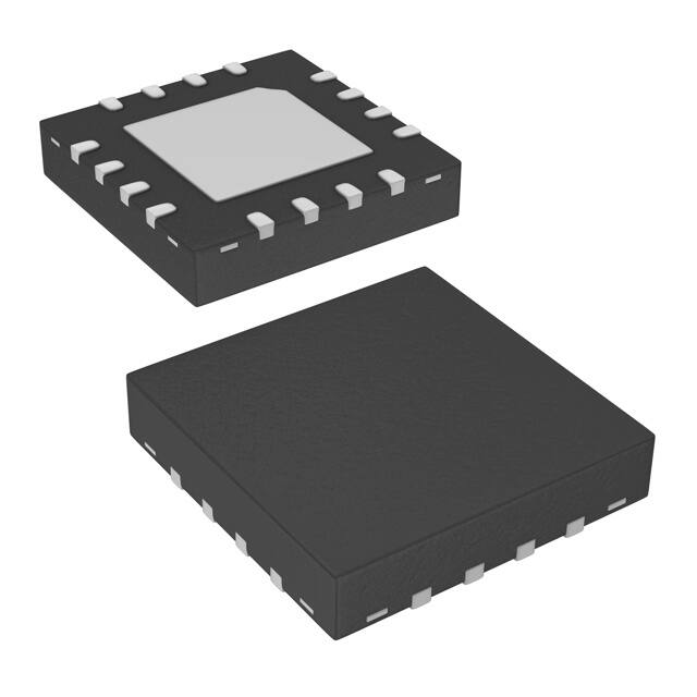
Pinout
VBAB
DISAB
VS+
OUTA
ISL1536
(16 LD 4X4 QFN)
TOP VIEW
3. For Moisture Sensitivity Level (MSL), please see device
information page for ISL1536. For more information on MSL,
please see tech brief TB363.
16
15
14
13
INA 1
12 OUTB
INB 2
11 NC
THERMAL
PAD*
GND 3
10 OUTC
9 OUTD
5
6
7
8
IND
VBCD
DISCD
VS-
INC 4
*GND FOR BOTH SINGLE/DUAL SUPPLY
FN6508 Rev 4.00
February 15, 2013
Page 1 of 9
�ISL1536
Block Diagram
INA
+
A
-
VS+
50k
VBAB
2RG
800
50k
VS-
7.5k
INB
INC
VS+
- 4.8k
B
+
OUTB
+
C
-
OUTC
2RG
800
50k
VS-
7.5k
IND
RF
4.8k
D
+
OUTD
LOGIC
CONTROL
DISAB
GND
LOGIC
CONTROL
RF
4.8k
DISCD
50k
VS-
RF
4.8k
RF
7.5k
VBCD
VS+
OUTA
7.5k
Pin Descriptions
16 LD QFN
PIN NAME
1
INA
Amplifier A input
2
INB
Amplifier B input
3
GND
Ground connection
4
INC
Amplifier C input
5
IND
Amplifier D input
6
VBCD
Voltage bias for amplifier C, D
7
DISCD
Enable/disable amplifiers C, D (DSL Channel #2)
8
VS-
9
OUTD
Amplifier D output
10
OUTC
Amplifier C output
11
NC
12
OUTB
Amplifier B output
13
OUTA
Amplifier A output
14
VS+
15
DISAB
Enable/disable amplifiers A, B (DSL Channel #1).
16
VBAB
Voltage bias for amplifier A, B
FN6508 Rev 4.00
February 15, 2013
FUNCTION
Negative supply
No internal connection. Connect to GND on PCB.
Positive supply
Page 2 of 9
�ISL1536
Absolute Maximum Ratings (TA = +25°C)
Thermal Information
VS+ to VS- Supply Voltage. . . . . . . . . . . . . . . . . . . . . . . . . . . . . .30V
VS+ Voltage to Ground . . . . . . . . . . . . . . . . . . . . . . . . -0.3V to +30V
VS- Voltage to Ground . . . . . . . . . . . . . . . . . . . . . . . . . . -30V to 0.3V
Input DISAB, DISCD to Ground . . . . . . . . . . . . . . . . . . . . . . . . . . .7V
VIN+ Voltage . . . . . . . . . . . . . . . . . . . . . . . . . . . . . . . . . . VS- to VS+
Current into any Input . . . . . . . . . . . . . . . . . . . . . . . . . . . . . . . . 8mA
Continuous Output Current . . . . . . . . . . . . . . . . . . . . . . . . . . . 75mA
ESD Rating
Human Body Model . . . . . . . . . . . . . . . . . . . . . . . . . . . . . . . . .4kV
Machine Model . . . . . . . . . . . . . . . . . . . . . . . . . . . . . . . . . . . .250V
Thermal Resistance (Typical, Note 4)
JA (°C/W)
16 Lead QFN . . . . . . . . . . . . . . . . . . . . . . . . . . . . . .
40
Ambient Operating Temperature Range . . . . . . . . . .-40°C to +85°C
Storage Temperature Range . . . . . . . . . . . . . . . . . .-60°C to +150°C
Operating Junction Temperature . . . . . . . . . . . . . . . . . . . . . . +150°C
Power Dissipation . . . . . . . . . . . . . . . . . . . . . . . . . . . . . . See curves
Pb-Free Reflow Profile. . . . . . . . . . . . . . . . . . . . . . . . .see link below
http://www.intersil.com/pbfree/Pb-FreeReflow.asp
CAUTION: Do not operate at or near the maximum ratings listed for extended periods of time. Exposure to such conditions may adversely impact product reliability and
result in failures not covered by warranty.
NOTE:
4. JA is measured with the component mounted on a high effective thermal conductivity test board in free air. See Tech Brief TB379 for details.
IMPORTANT NOTE: All parameters having Min/Max specifications are guaranteed. Typ values are for information purposes only. Unless otherwise noted, all tests are
at the specified temperature and are pulsed tests, therefore: TJ = TC = TA
Electrical Specifications
PARAMETER
VS = ±12V, RL = 50 to GND, DISAB = DISCD = 0, TA = +25°C, unless otherwise specified.
DESCRIPTION
CONDITIONS
MIN
(Note 5)
TYP
MAX
(Note 5)
UNIT
12.6
12.85
13.1
V/V
AC PERFORMANCE
AV
Gain
BW
-3dB Bandwidth
THD
Total Harmonic Distortion
SR
Slew Rate, Single-Ended Signal
50
MHz
f = 1MHz, VO = 10VoP-P - diff, RL = 50to GND
-69
dBc
f = 2.2MHz, VO = 10VoP-P - diff, RL = 50to GND
-59
dBc
400
V/µs
VOUT from -4.5V to +4.5V
200
DC PERFORMANCE
VOS-DM
Differential Mode Offset Voltage
-50
+50
mV
VOS-CM
Common Mode Offset Voltage
-125
125
mV
-5
+5
µA
INPUT CHARACTERISTICS
IB+
Non-Inverting Input Bias Current
eN
Input Noise Voltage
f = 10kHz
8.0
nV Hz
iN+
+Input Noise Current
f = 10kHz
1.0
pA/ Hz
RIN
Input Resistance
VIH
Input High Voltage
DIS inputs
VIL
Input Low Voltage
DIS inputs
IIH
Input High Current for DIS
DIS = 5V
20
IIL
Input Low Current for DIS
DIS = 0V
6
7.5
9
2.2
k
V
0.8
V
58
100
µA
-25
-7
0
µA
OUTPUT CHARACTERISTICS
VOUT-50
Loaded Output Swing Single-Ended
RL = 50 to GND
±10.4
±10.85
V
VOUT-30
Loaded Output Swing Single-Ended
RL = 30 to GND
±9.8
±10.4
V
VOUT-DIS
Disable Output Voltage
IOUT
Output Current
FN6508 Rev 4.00
February 15, 2013
±800
RL = 0
600
mV
mA
Page 3 of 9
�ISL1536
Electrical Specifications
PARAMETER
VS = ±12V, RL = 50 to GND, DISAB = DISCD = 0, TA = +25°C, unless otherwise specified. (Continued)
DESCRIPTION
MIN
(Note 5)
CONDITIONS
TYP
MAX
(Note 5)
UNIT
SUPPLY CHARACTERISTICS
VS(MAX)
Maximum Operating Supply Voltage
±13.2
V
VS(MIN)
Minimum Operating Supply Voltage
±7.5
V
IS+ (Enable)
Positive Supply Current per Amplifier All outputs at 0V, DIS = 0V
4.0
IS- (Enable)
Negative Supply Current per Amplifier All outputs at 0V, DIS = 0V
-4.85
IS+ (Power Down) Positive Supply Current per Amplifier All outputs at 0V, DIS = 5V
IS- (Power Down)
Negative Supply Current per Amplifier All outputs at 0V, DIS = 5V
IGND
GND Supply Current per Amplifier
-3.9
0.3
-0.75
All outputs at 0V
5
mA
mA
0.75
mA
0
mA
0.3
mA
NOTE:
5. Compliance to datasheet limits is assured by one or more methods: production test, characterization and/or design.
Typical Performance Curves
VS = ±12V
CL = 0pF
VS = ±6V
CL = 0pF
RL = 25
RL = 25
RL = 50
RL = 50
RL = 1k
RL = 100
FIGURE 1. DIFFERENTIAL FREQUENCY RESPONSE vs RL
VS = ±12V
RL = 100
68pF
RL = 1k
RL = 100
FIGURE 2. DIFFERENTIAL FREQUENCY RESPONSE vs RL
VS = ±6V
RL = 100
68pF
47pF
47pF
10pF
10pF
0pF
0pF
FIGURE 3. DIFFERENTIAL FREQUENCY RESPONSE vs CL
FN6508 Rev 4.00
February 15, 2013
FIGURE 4. DIFFERENTIAL FREQUENCY RESPONSE vs CL
Page 4 of 9
�ISL1536
Typical Performance Curves
(Continued)
VS = ±12V
RL = 100DIFF
VS = ±12V
RL = 100DIFF
HD2
HD2
HD3
HD3
FIGURE 5. 200kHz 2ND AND 3RD HARMONICS vs
DIFFERENTIAL OUTPUT VOLTAGE
FIGURE 6. 1MHz 2ND AND 3RD HARMONICS vs
DIFFERENTIAL OUTPUT VOLTAGE
VS = ±12V
RL = 100DIFF
PSRR-
HD2
PSRR+
HD3
FIGURE 7. 2.2MHz 2ND AND 3RD HARMONICS vs
DIFFERENTIAL OUTPUT VOLTAGE
FIGURE 8. PSRR vs FREQUENCY
(±VS
FIGURE 9. SUPPLY CURRENT vs SUPPLY VOLTAGE
(ALL AMPLIFIERS ENABLED)
FN6508 Rev 4.00
February 15, 2013
FIGURE 10. OUTPUT IMPEDANCE vs FREQUENCY
Page 5 of 9
�ISL1536
Typical Performance Curves
(Continued)
(±VS
FIGURE 11. DIFFERENTIAL 3dB BANDWIDTH vs SUPPLY
VOLTAGE
FIGURE 12. CHANNEL SEPARATION vs FREQUENCY
JEDEC JESD51-3 LOW EFFECTIVE THERMAL
CONDUCTIVITY TEST BOARD - THERMAL PAD
NOT CONNECTED TO BOARD
JEDEC JESD51-7 HIGH EFFECTIVE THERMAL
CONDUCTIVITY TEST BOARD - EXPOSED
DIEPAD SOLDERED TO PCB PER JESD51-5
4.5
1.2
POWER DISSIPATION (W)
POWER DISSIPATION (W)
4.0
1.0
833mW
0.8
0.6
QFN16
JA = +150°C/W
0.4
0.2
3.5
3.125W
3.0
QFN16
2.5
JA = +40°C/W
2.0
1.5
1.0
0.5
0
0
25
50
75 85 100
125
150
AMBIENT TEMPERATURE (°C)
FIGURE 13. PACKAGE POWER DISSIPATION vs AMBIENT
TEMPERATURE
FN6508 Rev 4.00
February 15, 2013
0
0
25
50
75 85 100
125
150
AMBIENT TEMPERATURE (°C)
FIGURE 14. PACKAGE POWER DISSIPATION vs AMBIENT
TEMPERATURE
Page 6 of 9
�ISL1536
Applications Information
Integrated Components
Product Description
The ISL1536 consists of two sets of high-power line driver
amplifiers that can be connected for full duplex differential line
transmission. The amplifiers are designed to be used with
ADSL2+ signals up to 2.2MHz. Each amplifier has identical
positive gain connections resulting in optimum common-mode
rejection. A typical interface circuit configuration is shown in
Figure 15.
DRIVER
INPUT
+
-
RB
RF*
TIP
RF*
ZLINE
RB
+
RECEIVER
OUTPUT +
RECEIVE
AMPLIFIERS
RECEIVER
OUTPUT -
The VBAB and VBCD pins also integrate a pair of 7.5k and
50k resistors on each port to bias the line driver for single
and dual supply usage. When powering the line driver with a
single supply, VBAB and VBCD pins are floated. When using
dual supplies, VBAB and VBCD pins are grounded.
Integration of these components in the line driver minimizes
assembly cost and board space.
Impedance Matching
RG*
DRIVER
INPUT
ISL1536 integrates bias and feedback resistors, minimizing the
number of external components. The gain is fixed at
+12.85V/V.
RF
R
+
RIN
+
-
R
RF
RIN
RING
RB in Figure 15 depends on the line impedance and
transformer’s turns ratio. Line impedance is characterized to
be 100across tip and ring. If a 1:N tranformer is used, RB
can be calculated according to Equation 1:
RB = 100
---------- 0.5
2
N
(EQ. 1)
*Values are internally
set for line driver
FIGURE 15. TYPICAL INTERFACE CIRCUIT CONFIGURATION
FN6508 Rev 4.00
February 15, 2013
Page 7 of 9
�ISL1536
Revision History
DATE
REVISION
November 20, 2012
FN6508.4
Added Note 3 to “Ordering Information” on page 1.
Changed HBM from 3kV to 4kV in “Absolute Maximum Ratings” on page 3.
Changed MM from 300V to 250V in “Absolute Maximum Ratings” on page 3
Added Note 5 to “Electrical Specifications” table on page 4.
March 8, 2010
FN6508.3
On page 4, changed the “Maximum Operating Supply Voltage” TYP from ±12.6V to ±13.2V
February 8, 2010
May 29, 2009
CHANGE
On page 3 in the “Electrical Specifications” table, changed VOUT-DIS Max spec from ±300mV to ±800mV
Added Revision History beginning from rev 3.
Changed the logic high level (VIH) on page 3 from Min 2.0V to Min 2.2V, which is consistent with the intended
applications (AFE output logic high levels are typically at 3.3V with 2.4V minimum) while providing added margin
to internal threshold variation.
On page 1 in the first paragraph, changed: "This device features a high drive capability of 400mA while
consuming only 3mA..." to "This device features a high drive capability of 400mA while consuming only 4mA...".
Added Theta JA and applicable note to “Thermal Information” on page 3.
Removed VS, Supply Voltage row in spec table. Added Maximum and Minimum Operating Supply Voltages
(VS(MAX) and VS(MIN)) with typical specs of ±12.6V and ±7.5V to “SUPPLY CHARACTERISTICS” on page 4.
Added “DISAB = DISCD = 0” to “Electrical Specifications” table common conditions.
© Copyright Intersil Americas LLC 2008-2013. All Rights Reserved.
All trademarks and registered trademarks are the property of their respective owners.
For additional products, see www.intersil.com/en/products.html
Intersil products are manufactured, assembled and tested utilizing ISO9001 quality systems as noted
in the quality certifications found at www.intersil.com/en/support/qualandreliability.html
Intersil products are sold by description only. Intersil may modify the circuit design and/or specifications of products at any time without notice, provided that such
modification does not, in Intersil's sole judgment, affect the form, fit or function of the product. Accordingly, the reader is cautioned to verify that datasheets are
current before placing orders. Information furnished by Intersil is believed to be accurate and reliable. However, no responsibility is assumed by Intersil or its
subsidiaries for its use; nor for any infringements of patents or other rights of third parties which may result from its use. No license is granted by implication or
otherwise under any patent or patent rights of Intersil or its subsidiaries.
For information regarding Intersil Corporation and its products, see www.intersil.com
FN6508 Rev 4.00
February 15, 2013
Page 8 of 9
�ISL1536
Package Outline Drawing
L16.4x4E
16 LEAD QUAD FLAT NO-LEAD PLASTIC PACKAGE
Rev 0, 4/08
4X 1.95
4.00
12X 0.65
A
B
13
6
PIN 1
INDEX AREA
6
PIN #1 INDEX AREA
16
1
12
4.00
2 . 50 ± 0 . 05
9
(4X)
4
0.15
5
8
TOP VIEW
0.10 M C A B
16X 0 . 4 ± 0 . 05
4 0.30 ± 0 . 05
BOTTOM VIEW
SEE DETAIL "X"
0.10 C
0.9±0.1
C
BASE PLANE
SEATING PLANE
0.08 C
( 3 . 8 TYP )
SIDE VIEW
( 2 . 50 TYP )
( 12X 0 . 65 )
C
0 . 2 REF
5
( 16X 0 .30 )
0 . 00 MIN.
0 . 05 MAX.
( 16 X 0 . 6 )
TYPICAL RECOMMENDED LAND PATTERN
DETAIL "X"
NOTES:
1. Dimensions are in millimeters.
Dimensions in ( ) for Reference Only.
2. Dimensioning and tolerancing conform to AMSE Y14.5m-1994.
3. Unless otherwise specified, tolerance : Decimal ± 0.05
4. Dimension b applies to the metallized terminal and is measured
between 0.15mm and 0.30mm from the terminal tip.
5. Tiebar shown (if present) is a non-functional feature.
6. The configuration of the pin #1 identifier is optional, but must be
located within the zone indicated. The pin #1 identifier may be
either a mold or mark feature.
FN6508 Rev 4.00
February 15, 2013
Page 9 of 9
�


 工商网监
湘ICP备2023018690号
工商网监
湘ICP备2023018690号
