DATASHEET
ISL26132, ISL26134
FN6954
Rev 3.00
November 20, 2014
Low-Noise 24-bit Delta Sigma ADC
Features
The ISL26132 and ISL26134 are complete analog front ends
for high resolution measurement applications. These 24-bit
Delta-Sigma Analog-to-Digital Converters include a very
low-noise amplifier and are available as either two or four
differential multiplexer inputs. The devices offer the same
pinout as the ADS1232 and ADS1234 devices and are
functionally compatible with these devices. The ISL26132 and
ISL26134 offer improved noise performance at 10Sps and
80Sps conversion rates.
• Up to 21.6 Noise-free bits
• Low noise amplifier with gains of 1x/2x/64x/128x
• RMS noise: 10.6nV @ 10Sps (PGA = 128x)
• Linearity error: 0.0002% FS
• Simultaneous rejection of 50Hz and 60Hz (@ 10Sps)
• Two (ISL26132) or four (ISL26134) channel differential
input multiplexer
The on-chip low-noise programmable-gain amplifier provides
gains of 1x/2x/64x/128x. The 128x gain setting provides an
input range of ±9.766mVFS when using a 2.5V reference. The
high input impedance allows direct connection of sensors, such
as load cell bridges to ensure the specified measurement
accuracy without additional circuitry. The inputs accept signals
100mV outside the supply rails when the device is set for unity
gain.
• On-chip temperature sensor (ISL26132)
• Automatic clock source detection
• Simple interface to read conversions
• +5V Analog, +5 to +2.7V digital supplies
• Pb-Free (RoHS compliant)
The Delta-Sigma ADC features a third order modulator
providing up to 21.6-bit noise-free performance. The device
can be operated from an external clock source, crystal
(4.9152MHz typical), or the on-chip oscillator.
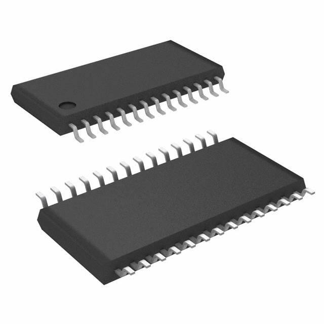
• TSSOP packages: ISL26132, 24 pin; ISL26134, 28 pin
The two channel ISL26132 is available in a 24 Ld TSSOP
package and the four channel ISL26134 is available in a 28 Ld
TSSOP package. Both are specified for operation over the
automotive temperature range (-40°C to +105°C).
• Temperature monitors and controls
Applications
• Weigh scales
• Industrial process control
• Pressure sensors
CAP
AVDD
DVDD
INTERNAL
CLOCK
EXTERNAL
OSCILLATOR
XTALIN/CLOCK
XTALOUT
AIN1+
AIN1SDO/RDY
AIN2+
AIN2-
ISL26134
Only
PGA
1x/2x/64x/
128x
INPUT
MULTIPLEXER
AIN3+
AIN3-
ADC
SCLK
AIN4+
AIN4PWDN
SPEED
A0
A1/TEMP
AGND
GAIN0 GAIN1
CAP
DGND
VREF+
VREF-
DGND
DGND
NOTE for A1/TEMP pin: Functions as A1 on ISL26134; Functions as TEMP on ISL26132
FIGURE 1. BLOCK DIAGRAM
FN6954 Rev 3.00
November 20, 2014
Page 1 of 23
�ISL26132, ISL26134
Ordering Information
PART NUMBER
(Notes 2, 3)
PART MARKING
TEMPERATURE RANGE
(°C)
PACKAGE
(Pb-free)
PKG.
DWG. #
ISL26132AVZ
26132 AVZ
-40 to +105
24 Ld TSSOP
M24.173
ISL26132AVZ-T (Note 1)
26132 AVZ
-40 to +105
24 Ld TSSOP (Tape & Reel) M24.173
ISL26132AVZ-T7A (Note 1)
26132 AVZ
-40 to +105
24 Ld TSSOP (Tape & Reel) M24.173
ISL26134AVZ
26134 AVZ
-40 to +105
28 Ld TSSOP
ISL26134AVZ-T (Note 1)
26134 AVZ
-40 to +105
28 Ld TSSOP (Tape & Reel) M28.173
ISL26134AVZ-T7A (Note 1)
26134 AVZ
-40 to +105
28 Ld TSSOP (Tape & Reel) M28.173
ISL26134AV28EV1Z
Evaluation Board
M28.173
NOTES:
1. Please refer to TB347 for details on reel specifications.
2. These Intersil Pb-free plastic packaged products employ special Pb-free material sets, molding compounds/die attach materials, and 100% matte
tin plate plus anneal (e3 termination finish, which is RoHS compliant and compatible with both SnPb and Pb-free soldering operations). Intersil
Pb-free products are MSL classified at Pb-free peak reflow temperatures that meet or exceed the Pb-free requirements of IPC/JEDEC J STD-020.
3. For Moisture Sensitivity Level (MSL), please see device information page for ISL26132, ISL26134. For more information on MSL please see techbrief
TB363.
TABLE 1. KEY DIFFERENCES OF PARTS
PART NUMBER
NUMBER OF CHANNELS
ON-CHIP TEMPERATURE SENSOR
NUMBER OF PINS
ISL26132
2
YES
24
ISL26134
4
NO
28
Pin Configurations
ISL26134
(28 LD TSSOP)
TOP VIEW
ISL26132
(24 LD TSSOP)
TOP VIEW
DVDD
1
24 SDO/RDY
DGND
2
23 SCLK
XTALIN/CLOCK
3
22 PDWN
XTALOUT
4
21 SPEED
DGND
5
20 GAIN1
DGND 5
24 GAIN1
DGND
6
19 GAIN0
DGND 6
23 GAIN0
TEMP
7
18 AVDD
A1 7
22 AVDD
A0
8
17 AGND
A0 8
21 AGND
CAP
9
16 VREF+
CAP 9
20 VREF+
CAP 10
15 VREF-
CAP 10
19 VREF-
AIN1+ 11
14 AIN2+
AIN1+ 11
18 AIN2+
AIN1- 12
13 AIN2-
AIN1- 12
17 AIN2-
AIN3+ 13
16 AIN4+
AIN3- 14
15 AIN4-
FN6954 Rev 3.00
November 20, 2014
DVDD 1
28 SDO/RDY
DGND 2
27 SCLK
XTALIN/CLOCK 3
26 PDWN
4
25 SPEED
XTALOUT
Page 2 of 23
�ISL26132, ISL26134
Pin Descriptions
PIN NUMBER
NAME
ISL26132
ISL26134
ANALOG/DIGITAL
INPUT/OUTPUT
DVDD
1
1
Digital
Digital Power Supply (2.7V to 5.25V)
Digital Ground
DGND
2, 5, 6
2, 5, 6
Digital
XTALIN/CLOCK
3
3
Digital/Digital Input
XTALOUT
4
4
Digital
TEMP
7
-
Digital Input
A1
A0
8
7
8
Digital Input
DESCRIPTION
External Clock Input: typically 4.9152MHz. Tie low to activate
internal oscillator. Can also use external crystal across
XTALIN/CLOCK and XTALOUT pins.
External Crystal connection
On-chip Temperature Diode Enable
TABLE 2. INPUT MULTIPLEXER SELECT
ISL26134
ISL26132
A1
A0
CHANNEL
0
0
AIN1
0
1
AIN2
1
0
AIN3
1
1
AIN4
CAP
9, 10
9, 10
Analog
AIN1+
11
11
Analog Input
Positive Analog Input Channel 1
AIN1-
12
12
Analog Input
Negative Analog Input Channel 1
AIN3+
-
13
Analog Input
Positive Analog Input Channel 3
AIN3-
-
14
Analog Input
Negative Analog Input Channel 3
AIN4-
-
15
Analog Input
Negative Analog Input Channel 4
AIN4+
-
16
Analog Input
Positive Analog Input Channel 4
AIN2-
13
17
Analog Input
Negative Analog Input Channel 2
AIN2+
14
18
Analog Input
Positive Analog Input Channel 2
VREF-
15
19
Analog Input
Negative Reference Input
VREF+
16
20
Analog Input
Positive Reference Input
AGND
17
21
Analog
Analog Ground
AVDD
18
22
Analog
Analog Power Supply 4.75V to 5.25V
GAIN0
GAIN1
19
20
23
24
Digital Input
FN6954 Rev 3.00
November 20, 2014
PGA Filter Capacitor
TABLE 3. GAIN SELECT
GAIN1
GAIN0
GAIN
0
0
1
0
1
2
1
0
64
1
1
128
Page 3 of 23
�ISL26132, ISL26134
Pin Descriptions (Continued)
PIN NUMBER
NAME
ISL26132
ISL26134
ANALOG/DIGITAL
INPUT/OUTPUT
SPEED
21
25
Digital Input
DESCRIPTION
TABLE 4. DATA RATE SELECT
SPEED
DATA RATE
0
10Sps
1
80Sps
PDWN
22
26
Digital Input
Power-Down: Holding this pin low powers down the entire
converter and resets the ADC.
SCLK
23
27
Digital Input
Serial Clock: Clock out data on the rising edge. Also used to
initiate Offset Calibration and Sleep modes. See “Serial Clock
Input (SCLK)” on page 14 for more details.
SDO/RDY
24
28
Digital Output
Dual-Purpose Output:
Data Ready: Indicate valid data by going low.
Data Output: Outputs data, MSB first, on the first rising edge
of SCLK.
Circuit Description
The ISL26132 (2-channel) and ISL26134 (4-channel) devices are
very low noise 24-bit delta-sigma ADCs that include a
programmable gain amplifier and an input multiplexer. The
ISL26132 offers an on-chip temperature measurement
capability.
The ISL26132, ISL26134 provide pin compatibility and output
data compatibility with the ADS1232/ADS1234, and offer the
same conversion rates of 10Sps and 80Sps.
All the features of the ISL26132, ISL26134 are pin-controllable,
while offset calibration, standby mode, and output conversion
data are accessible through a simple 2-wire interface.
The clock can be selected to come from an internal oscillator, an
external clock signal, or crystal (4.9152MHz typical).
FN6954 Rev 3.00
November 20, 2014
Page 4 of 23
�ISL26132, ISL26134
Absolute Maximum Ratings
Thermal Information
AGND to DGND . . . . . . . . . . . . . . . . . . . . . . . . . . . . . . . . . . . . . . -0.3V to +0.3V
Analog In to AGND . . . . . . . . . . . . . . . . . . . . . . . . . . . . . . . . -0.3 to AVDD+0.3V
Digital In to DGND . . . . . . . . . . . . . . . . . . . . . . . . . . . . . . . . -0.3 to DVDD+0.3V
Input Current
Momentary . . . . . . . . . . . . . . . . . . . . . . . . . . . . . . . . . . . . . . . . . . . . 100mA
Continuous . . . . . . . . . . . . . . . . . . . . . . . . . . . . . . . . . . . . . . . . . . . . . 10mA
ESD Rating
Human Body Model (Per MIL-STD-883 Method 3015.7) . . . . . . . . . . . . .7.5kV
Machine Model (Per JESD22-A115). . . . . . . . . . . . . . . . . . . . . . . . . . 450V
Charged Device Model (Per JESD22-C101) . . . . . . . . . . . . . . . . . . . . . . . . 2kV
Latch-up (Per JEDEC JESD-78C; Class 2, Level A)
. . . . . . . . . . . . . . . . . . . . . . . . . . . . . . . . 100mA @ Room and Hot (+105°C)
Thermal Resistance (Typical)
JA (°C/W) JC (°C/W)
24 Ld TSSOP (Notes 4, 5) . . . . . . . . . . . . . .
65
18
28 Ld TSSOP (Notes 4, 5) . . . . . . . . . . . . . .
63
18
Maximum Power Dissipation . . . . . . . . . . . . . . . . . . . . . . . . . . . . . . . . . . . . 80mW
Maximum Junction Temperature . . . . . . . . . . . . . . . . . . . . . . . . . . . .+150°C
Maximum Storage Temperature Range . . . . . . . . . . . . . .-65°C to +150°C
Pb-Free Reflow Profile . . . . . . . . . . . . . . . . . . . . . . . . . . . . . . . see link below
http://www.intersil.com/pbfree/Pb-FreeReflow.asp
Operating Conditions
Temperature Range . . . . . . . . . . . . . . . . . . . . . . . . . . . . . . .-40°C to +105°C
AVDD to AGND . . . . . . . . . . . . . . . . . . . . . . . . . . . . . . . . . . . . . .4.75V to 5.25V
DVDD to DGND . . . . . . . . . . . . . . . . . . . . . . . . . . . . . . . . . . . . . . . 2.7V to 5.25V
CAUTION: Do not operate at or near the maximum ratings listed for extended periods of time. Exposure to such conditions may adversely impact product
reliability and result in failures not covered by warranty.
NOTES:
4. JA is measured with the component mounted on a high effective thermal conductivity test board in free air. See Tech Brief TB379 for details.
5. For JC, the “case temp” location is taken at the package top center.
Electrical Specifications VREF+ = 5V, VREF- = 0V, AVDD = 5V, DVDD = 5V, AGND = DGND = 0V, MCLK = 4.9152MHz, and
TA = -40°C to +105°C, unless otherwise specified. Boldface limits apply over the operating temperature range, -40°C to +105°C
SYMBOL
PARAMETER
TEST LEVEL or NOTES
MIN
(Note 6)
TYP
MAX
(Note 6)
UNITS
ANALOG INPUTS
Differential Input Voltage Range
Common Mode Input Voltage
Range
Differential Input Current
±0.5VREF/
Gain
Gain = 1, 2
AGND - 0.1
Gain = 64, 128
AGND+1.5
V
AVDD + 0.1
AVDD - 1.5
V
V
Gain = 1
±20
nA
Gain = 2
±40
nA
Gain = 64, 128
±1
nA
80
SPS
SYSTEM PERFORMANCE
Resolution
No Missing Codes
Internal Osc. SPEED = High
Data Rate
Digital Filter Settling Time
INL
Integral Nonlinearity
Input Offset Error
Input Offset Drift
Gain Error (Note 8)
Gain Drift
FN6954 Rev 3.00
November 20, 2014
24
Bits
Internal Osc. SPEED = Low
10
SPS
External Osc. SPEED = High
fCLK/61440
SPS
External Osc. SPEED = Low
fCLK/491520
SPS
4
Conversions
Full Setting
Differential Input Gain = 1, 2
±0.0002
Differential Input Gain = 64, 128
±0.0004
±0.001
% of FSR (Note 7)
% of FSR (Note 7)
Gain = 1
±0.4
ppm of FS
Gain = 128
±1.5
ppm of FS
Gain = 1
0.3
µV/°C
Gain = 128
10
nV/°C
Gain = 1
±0.007
Gain = 128
±0.02
±0.02
%
%
Gain = 1
0.5
ppm/°C
Gain = 64
3.5
ppm/°C
Gain = 128
3.5
ppm/°C
Page 5 of 23
�ISL26132, ISL26134
Electrical Specifications VREF+ = 5V, VREF- = 0V, AVDD = 5V, DVDD = 5V, AGND = DGND = 0V, MCLK = 4.9152MHz, and
TA = -40°C to +105°C, unless otherwise specified. Boldface limits apply over the operating temperature range, -40°C to +105°C (Continued)
SYMBOL
CMRR
PSRR
PARAMETER
TEST LEVEL or NOTES
MIN
(Note 6)
TYP
85
100
MAX
(Note 6)
UNITS
Common Mode Rejection
AtDC, Gain = 1, V = 1V
At DC, Gain = 128, V = 0.1V
100
dB
50Hz/60Hz Rejection (Note 9)
External 4.9152MHz Clock
130
dB
Power Supply Rejection
dB
At DC, Gain = 1, V = 1V
82
100
dB
At DC, Gain = 128, V = 0.1V
100
105
dB
1.5
AVDD
Input Referred Noise
See “Typical Characteristics” beginning
on page 8
Noise Free Bits
See “Typical Characteristics” beginning
on page 8
VOLTAGE REFERENCE INPUT
VREF
Voltage Reference Input
VREF-
Negative Reference Input
VREF+
Positive Reference Input
IREF
VREF = VREF+ - VREF-
AVDD + 0.1
V
AGND - 0.1
VREF+ - 1.5
V
VREF- + 1.5
AVDD + 0.1
V
Voltage Reference Input Current
±350
nA
POWER SUPPLY REQUIREMENTS
AVDD
Analog Supply Voltage
4.75
5.0
5.25
V
DVDD
Digital Supply Voltage
2.7
3.3
5.25
V
AIDD
Analog Supply Current
Normal Mode, AVDD = 5, Gain = 1, 2
7
8.5
mA
Normal Mode, AVDD = 5, Gain = 64, 128
9
12
mA
DIDD
Digital Supply Current
Standby Mode
0.2
3
µA
Power-Down
0.2
2.5
µA
Normal Mode, AVDD = 5, Gain = 1, 2
750
950
µA
Normal Mode, AVDD = 5, Gain = 64, 128
750
950
µA
Standby Mode
1.5
26
µA
1
26
µA
49.6
mW
68
mW
Power-Down
PD
Power Dissipation, Total
Normal Mode, AVDD = 5, Gain = 1, 2
Normal Mode, AVDD = 5, Gain = 64, 128
Standby Mode
0.14
mW
Power-Down
0.14
mW
DIGITAL INPUTS
VIH
0.7 DVDD
V
0.2 DVDD
VIL
VOH
IOH = -1mA
DVDD - 0.4
V
IOL = 1mA
VOL
0.2 DVDD
V
±10
µA
Input Leakage Current
External Clock Input Frequency
Serial Clock Input Frequency
0.3
V
4.9152
MHz
1
MHz
NOTES:
6. Compliance to datasheet limits is assured by one or more methods: production test, characterization and/or design.
7. FSR = Full Scale Range = VREF/Gain
8. Gain accuracy is calibrated at the factory (AVDD = +5V).
9. Specified for word rate equal to 10Sps.
FN6954 Rev 3.00
November 20, 2014
Page 6 of 23
�ISL26132, ISL26134
Noise Performance
The ISL26132 and ISL26134 provide excellent noise
performance. The noise performance on each of the gain
settings of the PGA at the selected word rates is shown in
Tables 5 and 6.
Resolution in bits decreases by 1-bit if the ADC is operated as a
single-ended input device. Noise measurements are
input-referred, taken with bipolar inputs under the specified
operating conditions, with fCLK = 4.9152MHz.
TABLE 5. AVDD = 5V, VREF = 5V, DATA RATE = 10Sps
GAIN
RMS NOISE
(nV)
PEAK-TO-PEAK NOISE
(nV) (Note 10)
NOISE-FREE BITS
(Note 11)
1
243
1604
21.6
2
148
977
21.3
64
11.3
75
20
128
10.6
70
19
TABLE 6. AVDD = 5V, VREF = 5V, DATA RATE = 80Sps
GAIN
RMS NOISE
(nV)
PEAK-TO-PEAK NOISE
(nV) (Note 10)
NOISE-FREE BITS
(Note 11)
1
565
3730
20.4
2
285
1880
20.3
64
29.5
194.8
18.6
128
28.2
186.1
17.6
NOTES:
10. The peak-to-peak noise number is 6.6 times the rms value. This
encompasses 99.99% of the noise excursions that may occur. This
value best represents the worst case noise that could occur in the
output conversion words from the converter.
11. Noise-Free Bits is defined as: Noise-Free Bits = ln(FSR/peak-to-peak
noise)/ln(2) where FSR is the full scale range of the converter,
VREF/Gain.
FN6954 Rev 3.00
November 20, 2014
Page 7 of 23
�ISL26132, ISL26134
Typical Characteristics
300
10
GAIN = 1, N = 1024
GAIN = 1
RATE = 10Sps
RATE = 10Sps
250
STD DEV = 1.635 LSB
VREF = 2.5V
200
COUNTS
OUTPUT CODE (LSB)
5
0
150
100
-5
50
-10
0
200
400
600
800
0
1000
-7
-6
-5
-4
FIGURE 2. NOISE AT GAIN = 1, 10Sps
10
-2
-1
0
1
2
3
4
5
6
7
FIGURE 3. NOISE HISTOGRAM AT GAIN = 1, 10Sps
250
GAIN = 2
RATE = 10Sps
GAIN = 2, N = 1024
RATE = 10Sps
STD DEV = 1.989 LSB
VREF = 2.5V
200
COUNTS
5
OUTPUT CODE (LSB)
-3
OUTPUT CODE (LSB)
TIME (SAMPLES)
0
150
100
-5
50
-10
0
200
400
600
TIME (SAMPLES)
800
0
1000
FIGURE 4. NOISE AT GAIN = 2, 10Sps
120
GAIN = 64
RATE = 10Sps
15
-6
-4
-2
0
2
OUTPUT CODE (LSB)
4
6
8
FIGURE 5. NOISE HISTOGRAM AT GAIN = 2, 10Sps
20
100
10
GAIN = 64, N = 1024
RATE = 10Sps
STD DEV = 4.627 LSB
VREF = 2.5V
80
5
COUNTS
OUTPUT CODE (LSB)
-8
0
60
40
-5
20
-10
-15
0
200
400
600
800
TIME (SAMPLES)
FIGURE 6. NOISE AT GAIN = 64, 10Sps
FN6954 Rev 3.00
November 20, 2014
1000
0
-20
-15
-10
-5
0
5
OUTPUT CODE (LSB)
10
15
20
FIGURE 7. NOISE HISTOGRAM AT GAIN = 64, 10Sps
Page 8 of 23
�ISL26132, ISL26134
Typical Characteristics (Continued)
50
60
GAIN = 128
RATE = 10Sps
GAIN = 128, N = 1024
RATE = 10Sps
50
30
STD DEV = 8.757 LSB
40
10
COUNTS
OUTPUT CODE (LSB)
VREF = 2.5V
-10
30
20
-30
-50
10
0
200
400
600
800
0
1000
-30 -25 -20 -15 -10
TIME (SAMPLES)
FIGURE 8. NOISE AT GAIN = 128, 10Sps
0
5
10
15
20
25
30
FIGURE 9. NOISE HISTOGRAM AT GAIN = 128, 10Sps
25
120
GAIN = 1
RATE = 80Sps
20
-5
OUTPUT CODE (LSB)
GAIN = 1, N = 1024
RATE = 80Sps
100 STD DEV = 3.791 LSB
15
80
5
COUNTS
OUTPUT CODE (LSB)
VREF = 2.5V
10
0
-5
60
40
-10
-15
20
-20
-25
0
200
400
600
800
0
-15
1000
-10
0
5
10
15
FIGURE 11. NOISE HISTOGRAM AT GAIN = 1, 80Sps
FIGURE 10. NOISE AT GAIN = 1, 80Sps
120
25
GAIN = 2
RATE = 80Sps
GAIN = 2, N = 1024
RATE = 80Sps
100
15
STD DEV = 3.831 LSB
VREF = 2.5V
80
5
COUNTS
OUTPUT CODE (LSB)
-5
OUTPUT CODE (LSB)
TIME (SAMPLES)
-5
60
40
-15
-25
20
0
200
400
600
TIME (SAMPLES)
800
FIGURE 12. NOISE AT GAIN = 2, 80Sps
FN6954 Rev 3.00
November 20, 2014
1000
0
-15
-10
-5
0
5
OUTPUT CODE (LSB)
10
FIGURE 13. NOISE HISTOGRAM AT GAIN = 2, 80Sps
Page 9 of 23
15
�ISL26132, ISL26134
Typical Characteristics (Continued)
100
50
GAIN = 64, N = 1024
GAIN = 64
RATE = 80Sps
RATE = 80Sps
COUNTS
OUTPUT CODE (LSB)
STD DEV = 12.15 LSB
40
50
0
VREF = 2.5V
30
20
-50
10
-100
0
200
400
600
800
0
-40 -35 -30 -25 -20 -15 -10 -5
1000
FIGURE 14. NOISE AT GAIN = 64, 80Sps
30
GAIN = 128
RATE = 80Sps
GAIN = 128, N = 1024
RATE = 80Sps
25
80
OUTPUT CODE (LSB)
5 10 15 20 25 30 35 40
FIGURE 15. NOISE HISTOGRAM AT GAIN = 64, 80Sps
160
120
0
OUTPUT CODE (LSB)
TIME (SAMPLES)
STD DEV = 23.215 LSB
VREF = 2.5V
40
COUNTS
20
0
-40
-80
15
10
-120
5
-160
-200
0
200
400
600
TIME (SAMPLES)
800
0
-80
1000
FIGURE 16. NOISE AT GAIN = 128, 80Sps
-40
-20
0
20
OUTPUT CODE (LSB)
40
60
80
FIGURE 17. NOISE HISTOGRAM AT GAIN = 128, 80Sps
10000
10
8
NORMAL MODE, PGA = 64.128
1000
CURRENT (µA)
CURRENT (mA)
-60
6
NORMAL MODE, PGA = 1, 2
4
NORMAL MODE, ALL PGA GAINS
100
10
2
0
-40
-10
20
50
80
TEMPERATURE (°C)
FIGURE 18. ANALOG CURRENT vs TEMPERATURE
FN6954 Rev 3.00
November 20, 2014
110
POWERDOWN MODE
1
-40
-10
20
50
80
TEMPERATURE (°C)
FIGURE 19. DIGITAL CURRENT vs TEMPERATURE
Page 10 of 23
110
�ISL26132, ISL26134
Typical Characteristics (Continued)
10000
11.0
WORD RATE = 10Sps
GAIN = 1, 80Sps
64k FFT
25 AVERAGES
10.8
NOISE (nV/√Hz)
DATA RATE (Sps)
10.6
10.4
10.2
1000
100
10.0
9.8
9.6
-40
-10
20
50
TEMPERATURE (°C)
80
10
110
FIGURE 20. TYPICAL WORD RATE vs TEMPERATURE USING
INTERNAL OSCILLATOR
0.01
0.1
1
FREQUENCY (Hz)
10
FIGURE 21. NOISE DENSITY vs FREQUENCY AT GAIN = 1, 80Sps
100
NOISE (nV/√Hz)
GAIN = 128, 80Sps
64k FFT
25 AVERAGES
10
1
0.01
0.1
1
10
FREQUENCY (Hz)
FIGURE 22. NOISE DENSITY vs FREQUENCY AT GAIN = 128, 80Sps
FN6954 Rev 3.00
November 20, 2014
Page 11 of 23
�ISL26132, ISL26134
Functional Description
Analog Inputs
The analog signal inputs to the ISL26132 connect to a 2-Channel
differential multiplexer and the ISL26134 connect to a 4-Channel
differential multiplexer (Mux). The multiplexer connects a pair of
inputs to the positive and negative inputs (AINx+, AINx-), selected
by the Channel Select Pins A0 and A1 (ISL26134 only). Input
channel selection is shown in Table 7. On the ISL26132, the
TEMP pin is used to select the Temperature Sensor function.
If the differential input exceeds well above the +VE or the -VE FS
(by ~1.5x times) the output code will clip to the corresponding FS
value. Under such conditions, the output data rate will become
1/4th of the original value as the Digital State Machine will
RESET the Delta-Sigma Modulator and the Decimation Filter.
Temperature Sensor (ISL26132 only)
TABLE 7. INPUT CHANNEL SELECTION
CHANNEL SELECT PINS
The input span of the ADC is ±0.5 VREF/GAIN. For a 5V VREF and
a gain of 1x, the input span will be 5VP-P fully differential as
shown in Figure 23. Note that input voltages that exceed the
supply rails by more than 100mV will turn on the ESD protection
diodes and degrade measurement accuracy.
ANALOG INPUT PINS SELECTED
A1
A0
AIN+
AIN-
0
0
AIN1+
AIN1-
0
1
AIN2+
AIN2-
When the TEMP pin of the ISL26132 is set High, the input
multiplexer is connected to a pair of diodes, which are scaled in
both size and current. The voltage difference measured between
them corresponds to the temperature of the die according to
Equation 1:
1
0
AIN3+
AIN3-
V = 102.2mV + (379V T C ) Gain
1
1
AIN4+
AIN4-
(EQ. 1)
Note: Valid only for GAIN = 1x or 2x
Whenever the MUX channel is changed (i.e. if any one of the
following inputs - A0/A1, Gain1/0, SPEED is changed), the
digital logic will automatically restart the digital filter and will
cause SDO/RDY to go low only when the output is fully settled.
But if the input itself is suddenly changed, then the user needs to
ignore the first four RDY pulses (going low) to get an accurate
measurement of the input signal.
1.25V
Where T is the temperature of the die, and Gain = the PGA Gain
Setting.
At a temperature of +25°C, the measured voltage will be
approximately 111.7mV. Note that this measurement indicates
only the temperature of the die itself. Applying the result to
correct for the temperature drift of a device external to the
package requires that thermal coupling between the sensor and
the die be taken into account.
Low-Noise Programmable Gain Amplifier
(PGA)
3.75
2.50
AIN+
1.25
INPUT VOLTAGE RANGE = ±0.5VREF/GAIN
VREF = 5V, GAIN = 1X
3.75
2.50
AIN-
The chopper-stabilized programmable gain amplifier features a
variety of gain settings to achieve maximum dynamic range and
measurement accuracy from popular sensor types with excellent
low noise performance, input offset error, and low drift, and with
minimal external parts count. The GAIN0 and GAIN1 pins allow the
user to select gain settings of 1x, 2x, 64x, or 128x. A block diagram
is shown in Figure 24. The differential input stage provides a gain of
64, which is bypassed when the lower gain settings are selected.
The lower gain settings (1 and 2) will accept inputs with common
mode voltages up to 100mV outside the rails, allowing the device to
accept ground-referred signals. At gain settings of 64 or 128 the
common mode voltage at the inputs is limited to 1.5V inside the
supply rails while maintaining specified measurement accuracy.
1.25
2.50V
FIGURE 23. DIFFERENTIAL INPUT FOR VREF = 5V, GAIN = 1X
FN6954 Rev 3.00
November 20, 2014
Page 12 of 23
�ISL26132, ISL26134
CAP
AINx+
+
RINT
A1
RF1
R1
ADC
RF2
A2
AINx-
RINT
+
CAP
FIGURE 24. SIMPLIFIED PROGRAMMABLE GAIN AMPLIFIER BLOCK DIAGRAM
Filtering PGA Output Noise
The programmable gain amplifier, as shown in Figure 24,
includes a passive RC filter on its output. The resistors are
located inside the chip on the outputs of the differential amplifier
stages. The capacitor (nominally a 100nF C0G ceramic or a PPS
film (Polyphenylene sulfide)) for the filter is connected to the two
CAP pins of the chip. The outputs of the differential amplifier
stages of the PGA are filtered before their signals are presented
to the delta-sigma modulator. This filter reduces the amount of
noise by limiting the signal bandwidth and filters the chopping
artifacts of the chopped PGA stage.
If the ADC is to be operated from a crystal, it should be located
close to the package pins of the ADC. Note that external loading
capacitors for the crystal are not required as there are loading
capacitors built into the silicon, although the capacitor values are
optimized for operation with a 4.9152MHz crystal.
The XTALOUT pin is not intended to drive external circuits.
XTALIN/
CLOCK
CRYSTAL
OSCILLATOR
CLOCK DETECT
Voltage Reference Inputs (VREF+, VREF-)
The voltage reference for the ADC is derived from the difference
in the voltages presented to the VREF+ and VREF- pins;
VREF = (VREF+ - VREF-). The ADCs are specified with a voltage
reference value of 5V, but a voltage reference as low as 1.5V can
be used. For proper operation, the voltage on the VREF+ pin
should not be greater than AVDD + 0.1V and the voltage on the
VREF- pin should not be more negative than AGND - 0.1V.
INTERNAL
EN
OSCILLATOR
XTALOUT
MUX
TO ADC
FIGURE 25. CLOCK BLOCK DIAGRAM
Clock Sources
Digital Filter Characteristics
The ISL26132, ISL26134 can operate from an internal oscillator,
an external clock source, or from a crystal connected between
the XTALIN/CLOCK and XTALOUT pins. See the block diagram of
the clock system in Figure 25. When the ADC is powered up, the
CLOCK DETECT block determines if an external clock source is
present. If a clock greater than 300kHz is present on the
XTALIN/CLOCK pin, the circuitry will disable the internal oscillator
on the chip and use the external clock as the clock to drive the
chip circuitry. If the ADC is to be operated from the internal
oscillator, the XTALIN/CLOCK pin should be grounded.
The digital filter inside the ADC is a fourth-order Sinc filter.
Figures 26 and 27 on page 14 on illustrate the filter response for
the ADC when it is operated from a 4.9152MHz crystal. The
internal oscillator is factory trimmed so the frequency response
for the filter will be much the same when using the internal
oscillator. The figures illustrate that when the converter is
operated at 10Sps the digital filter provides excellent rejection of
50Hz and 60Hz line interference.
FN6954 Rev 3.00
November 20, 2014
Page 13 of 23
�ISL26132, ISL26134
Serial Clock Input (SCLK)
0
The serial clock input is provided with hysteresis to minimize
false triggering. Nevertheless, care should be taken to ensure
reliable clocking.
DATA RATE = 10
10Sps
SPS
-50
GAIN (dB)
Filter Settling Time and ADC Latency
Whenever the analog signal into the ISL26132, ISL26134
converters is changed, the effects of the digital filter must be
taken into account. The filter takes four data ready periods for
the output code to fully reflect a new value at the analog input. If
the multiplexer control input is changed, the modulator and the
digital filter are reset, and the device uses four data ready
periods to fully settle to yield a digital code that accurately
represents the analog input. Therefore, from the time the control
inputs for the multiplexer are changed until the SDO/RDY goes
low, four data ready periods will elapse. The settling time delay
after a multiplexer channel change is listed in Table 8 for the
converter operating in continuous conversion mode. This is also
shown pictorially in Figure 28 for a change in the MUX setting
and Figure 29 for an abrupt change in the analog input VIN.
-100
-150
0
10
20
30 40 50 60 70
FREQUENCY (Hz)
80
90 100
FIGURE 26. 10Sps: FREQUENCY RESPONSE OUT TO 100Hz
-50
-60
DATA RATE = 10Sps
-70
GAIN (dB)
-80
-90
-100
-110
-120
-130
-140
-150
45
50
55
FREQUENCY (Hz)
65
60
FIGURE 27. 10Sps: 50/60Hz NOISE REJECTION, 45Hz TO 65Hz
TABLE 8. SETTLING TIME
DESCRIPTION
(fCLK = 4.9152MHz)
PARAMETER
tS
t1
MIN
MAX
UNITS
40
50
µs
SPEED = 1
54
55
ms
SPEED = 0
404
405
ms
A0, A1, SPEED, Gain1, Gain0 change
set-up time
Settling time
A0, A1, SPEED, Gain1, Gain0
t1
SDO/RDY
tS
FIGURE 28. SDO/RDY DELAY AFTER MULTIPLEXER CHANGE
FN6954 Rev 3.00
November 20, 2014
Page 14 of 23
�ISL26132, ISL26134
Abrupt Change in External VIN
VIN
1st conversion;
includes
unsettled VIN
Start of
conversion
SDO/RDY
2nd conversion;
VIN settled,
Digital filter
unsettled
3rd conversion;
VIN settled,
Digital filter
unsettled
4th conversion;
VIN settled,
Digital filter
unsettled
5th conversion;
VIN and Digital,
filter settled
Conversion
time
FIGURE 29. SDO/RDY DELAY AFTER MULTIPLEXER CHANGE
Conversion Data Rate
Reading Conversion Data from the Serial
Data Output/Ready SDO/RDY Pin
The SPEED pin is used to select between the 10Sps and 80Sps
conversion rates. The 10Sps rate (SPEED = Low) is preferred in
applications requiring 50/60Hz noise rejection. Note that the
sample rate is directly related to the oscillator frequency, as
491,520 clocks are required to perform a conversion at the
10Sps rate, and 61,440 clocks at the 80Sps rate.
Output Data Format
The 24-bit converter output word is delivered in two’s
complement format. Input exceeding full scale results in a
clipped output which will not return to in-range values until after
the input signal has returned to the specified allowable voltage
range and the digital filter has settled as discussed previously.
TABLE 9. OUTPUT CODES CORRESPONDING TO INPUT
INPUT SIGNAL
OUTPUT CODE (HEX)
+0.5VREF/GAIN
7FFFFF
(+0.5VREF/GAIN)/(223 - 1)
000001
0
000000
(-0.5VREF/GAIN)/(223 - 1)
FFFFFF
-0.5VREF/GAIN
800000
When the ADC is powered, it will automatically begin doing
conversions. The SDO/RDY signal will go low to indicate the
completion of a conversion. After the SDO/RDY signal goes low,
the MSB data bit of the conversion word will be output from the
SDO/RDY pin after SCLK is transitioned from a low to a high.
Each subsequent new data bit is also output on the rising edge of
SCLK (see Figure 30). The receiving device should use the falling
edge of SCLK to latch the data bits. After the 24th SCLK, the
SDO/RDY output will remain in the state of the LSB data bit until
a new conversion is completed. At this time, the SDO/RDY will go
high if low and then go low to indicate that a new conversion
word is available. If not all data bits are read from the SDO/RDY
pin prior to the completion of a new conversion, they will be
overwritten. SCLK should be low during time t6, as shown in
Figure 30, when SDO/RDY is high.
If the user wants the SDO/RDY signal to go high after reading the
24 bits of the conversion data word, a 25th SCLK can be issued.
The 25th SCLK will force the SDO/RDY signal to go high and
remain high until it falls to signal that a new conversion word is
available. Figure 31 illustrates the behavior of the SDO/RDY
signal when a 25th SCLK is used.
DATA
DATA READY
NEW DATA READY
MSB
SDO/RDY
23
LSB
22
0
21
t5
t4
SCLK
t6
t3
t2
24
1
t3
t7
FIGURE 30. OUTPUT DATA WAVEFORMS USING 24 SCLKS TO READ CONVERSION DATA
FN6954 Rev 3.00
November 20, 2014
Page 15 of 23
�ISL26132, ISL26134
TABLE 10. INTERFACE TIMING CHARACTERISTICS
PARAMETER
DESCRIPTION
MIN
t2
SDO/RDY Low to first SLK
0
100
TYP
MAX
UNITS
ns
t3
SCLK pulsewidth, Low or High
t4
SCLK High to Data Valid
t5
Data Hold after SCLK High
0
ns
t6
Register Update Time
39
µs
Conversion Period
t7
ns
50
ns
SPEED = 1
12.5
ms
SPEED = 0
100
ms
DATA
DATA READY
NEW DATA READY
SDO/RDY
23
22
21
0
25TH SCLK FORCES
SCLK
24
1
SDO/RDY HIGH
25
FIGURE 31. OUTPUT DATA WAVEFORMS FOR SDO/RDY POLLING
DATA READY AFTER CALIBRATION
SDO/RDY
23
22
21
23
0
CALIBRATION BEGINS
SCLK
1
24
25
26
t8
FIGURE 32. OFFSET CALIBRATION WAVEFORMS
Offset Calibration Control
The offset internal to the ADC can be removed by performing an
offset calibration operation. Offset calibration can be initiated
immediately after reading a conversion word with 24 SCLKs by
issuing two additional SCLKs. The offset calibration operation will
begin immediately after the 26th SCLK occurs. Figure 32
illustrates the timing details for the offset calibration operation.
During offset calibration, the analog inputs are shorted internally
and a regular conversion is performed. This conversion generates
a conversion word that represents the offset error. This value is
stored and used to digitally remove the offset error from future
conversion words. The SDO/RDY output will fall to indicate the
completion of the offset calibration operation.
TABLE 11. SDO/RDY DELAY AFTER CALIBRATION
PARAMETER
t8
MIN
MAX
UNITS
SPEED = 1
108
109
ms
SPEED = 0
808
809
ms
Standby Mode Operation
The ADC can be put into standby mode to save power. Standby
mode reduces the power to all circuits in the device except the
FN6954 Rev 3.00
November 20, 2014
crystal oscillator amplifier. To enter the standby mode, take the
SCLK signal high and hold it high after SDO/RDY falls. The
converter will remain in standby mode as long as SCLK is held
high. To return to normal operation, take SCLK back low and wait
for the SDO/RDY to fall to indicate that a new conversion has
completed. Figure 33 and Table 12 illustrate the details of
standby mode.
Supply currents are equal in Standby and Power-down modes
unless a Crystal is used. If the Crystal is used, the Crystal
amplifier is turned ON, even in the standby mode.
Performing Offset Calibration After Standby
Mode
To perform an offset calibration automatically upon returning
from standby, deliver two or more additional SCLKs following a
data read cycle, and then set and hold SCLK high. The device will
remain in Standby as long as SCLK remains high. A calibration
cycle will begin once SCLK is brought low again to resume
normal operation. Additional time will be required to perform the
calibration after returning from Standby. Figure 34 and Table 13
illustrate the details of performing offset calibration after
standby mode.
Page 16 of 23
�ISL26132, ISL26134
STANDBY MODE
23
SDO/RDY
22
21
DATA READY
23
0
START
CONVERSION
SCLK
1
24
t9
t11
t10
FIGURE 33. STANDBY MODE WAVEFORMS
TABLE 12. STANDBY MODE TIMING
PARAMETER
DESCRIPTION
t9
SCLK High after
SDO/RDY Low
Standby Mode Delay
t10
t11
SDO/RDY falling edge
after SCLK Low
MIN
MAX
UNITS
SPEED = 1
0
12.44
ms
SPEED = 0
0
99.94
ms
SPEED = 1
12.5
SPEED = 0
100
SPEED = 1
50
60
ms
SPEED = 0
400
410
ms
ms
ms
TABLE 13. OFFSET CALIBRATION TIMING AFTER STANDY
PARAMETER
DESCRIPTION
t12
SDO/RDY Low after
SCLK Low
MIN
MAX
UNITS
SPEED = 1
108
113
ms
SPEED = 0
808
813
ms
STANDBY MODE
SDO/RDY
SCLK
23
22
21
0
1
24
t10
DATA READY AFTER CALIBRATION
BEGIN
CALIBRATION
23
25
t12
FIGURE 34. OFFSET CALIBRATION WAVEFORMS AFTER STANDBY
FN6954 Rev 3.00
November 20, 2014
Page 17 of 23
�ISL26132, ISL26134
Operation of PDWN
AVDD
PDWN must transition from low to high after both power supplies
have settled to specified levels in order to initiate a correct
power-up reset (Figure 35). This can be implemented by an
external controller or a simple RC delay circuit, as shown in
Figure 36.
DVDD
PDWN
10µs
In order to reduce power consumption, the user can assert the
Power-down mode by bringing PDWN Low as shown in Figure 37.
All circuitry is shut down in this mode, including the Crystal
Oscillator. After PDWN is brought High to resume operation, the
reset delay varies depending on the clock source used. While an
external clock source will resume operation immediately, a
circuit utilizing a crystal will incur about a 20ms delay due to the
inherent start-up time of this type of oscillator.
FIGURE 35. POWER-DOWN TIMING RELATIVE TO SUPPLIES
DVDD
1k
CONNECT TO
2.2nF
PDWN PIN
FIGURE 36. PDWNDELAY CIRCUIT
POWER-DOWN
MODE
CLK
SOURCE
WAKEUP
START
CONVERSION
DATA
READY
t14
t14
PDWN
SDO/RDY
t13
t11
SCLK
FIGURE 37. POWER-DOWN MODE WAVEFORMS
TABLE 14. POWER-DOWN RECOVERY TIMING
PARAMETER
DESCRIPTION
t13
Clock Recovery after PDWN
High
t14
FN6954 Rev 3.00
November 20, 2014
PDWN Pulse Duration
TYP
UNITS
Internal Oscillator
7.95
µs
External Clock Source
0.16
µs
4.9152MHz Crystal
Oscillator
5.6
ms
26
µs (min)
Page 18 of 23
�ISL26132, ISL26134
Application Information
Application Examples
Power-up Sequence – Initialization and
Configuration
WEIGH SCALE SYSTEM
Figure 38 illustrates the ISL26132 connected to a load cell. The
A/D converter is configured for a gain of 128x and a sample rate
of 10Sps. If a load cell with 2mV/V sensitivity is used, the full
scale output from the load cell will be 10mV. On a gain of 128x
and sample rate of 10Sps, the converter noise is 67nVP-P. The
converter will achieve 10mV/67nVP-P = 149,250 noise free
counts across its 10mV input signal. This equates to 14,925
counts per millivolt of input signal. If five output words are
averaged together this can be improved by √5 to yield √5*14925
counts = 33,370 counts per millivolt of input signal with an
effective update rate of 2 readings per second.
The sequence to properly power-up and initialize the device are
as follows. For details on individual functions, refer to their
descriptions.
1. AVDD, DVDD ramp to specified levels
2. Apply External Clock
3. Pull PDWN High to initiate Reset
4. Device begins conversion
5. SDO/RDY goes low at end of first conversion
OPTIONAL ACTIONS
• Perform Offset Calibration
• Place device in Standby
• Return device from Standby
• Read on-chip Temperature (applicable to ISL26132 only)
5V
3V
0.1µF
18
AVDD
16
9
-
+
1
DVDD
GAIN1
VREF+
CAP
GAIN0
SDO/RDY
0.1µF
10 CAP
SCLK
ISL26132
VDD
20
19
24
GAIN = 128
23
22
PDWN
4
XTALOUT
11 AIN+1
12
AIN-1
3
14
XTALIN/CLOCK
AIN+2
21
SPEED
13 AIN-2
A0 8
15
7
VREFTEMP
AGND
DGND
17
MICRO
CONTROLLER
GND
2, 5, 6
FIGURE 38. WEIGH SCALE APPLICATION
FN6954 Rev 3.00
November 20, 2014
Page 19 of 23
�ISL26132, ISL26134
+5V
+3V
0.1µF
0.1µF
5M
18
AVDD
ISL21009
4.096V
16
1
DVDD
GAIN1
VREF+
10nF
GAIN0
SDO/RDY
SCLK
10k
TYPE K
PDWN
11 AIN+1
10k
12
1µF
14
XTALOUT
AIN-1
AIN+2
XTALIN/CLOCK
13 AIN-2
5M
15
VREFAGND
17
20
19
24
22
4
3
SPEED 21
A0 8
TEMP
DGND
MICRO
CONTROLLER
23
4.9152
MHz
7
2, 5, 6
FIGURE 39. THERMOCOUPLE MEASUREMENT APPLICATION
THERMOCOUPLE MEASUREMENT
Figure 39 illustrates the ISL26132 in a thermocouple
application. The 4.096V reference combined with the PGA gain
set to 128x sets the input span of the converter to ±16mV. This
supports the K type thermocouple measurement for
temperatures from -270°C at -6.485mV to +380°C at about
16mV.
If a higher temperature is preferred, the PGA can be set to 64x to
provide a converter span of ±32mV. This will allow the converter
to support temperature measurement with the K type
thermocouple up to about +765°C.
Figure 39 shows that the thermocouple is referenced to a voltage
dictated by the resistor divider from the +5V supply to ground.
These set the common mode voltage at about 2.5V. The 5M
resistors provide a means for detection of an open thermocouple.
If the thermocouple fails to open or is not connected, the bias
through the 5M resistors will cause the input to the PGA to go to
full scale.
PCB Board Layout and System
Configuration
The ISL26132, ISL26134 ADC is a very low noise converter. To
achieve the full performance available from the device will
require attention to the printed circuit layout of the circuit board.
Care should be taken to have a full ground plane without
impairments (traces running through it) directly under the chip
on the back side of the circuit board. The analog input signals
should be laid down adjacent (AIN+ and AIN- for each channel) to
achieve good differential signal practice and routed away from
any traces carrying active digital signals. The connections from
the CAP pins to the off-chip filter capacitor should be short, and
without any digital signals nearby. The crystal, if used, should be
connected with relatively short leads. No active digital signals
should be routed near or under the crystal case or near the
traces, which connect it to the ADC. The AGND and DGND pins of
the ADC should be connected to a common solid ground plane.
All digital signals to the chip should be powered from the same
supply, as that used for DVDD (do not allow digital signals to be
active high unless the DVDD supply to the chip is alive). Route all
active digital signals in a way to keep distance from any analog
pin on the device (AIN, VREF, CAP, AVDD). Power on the AVDD
supply should be active before the VREF voltage is present.
PCB layout patterns for the chips (ISL26132 and ISL26134) are
found on the respective package outline drawings on pages 22
and 23.
FN6954 Rev 3.00
November 20, 2014
Page 20 of 23
�ISL26132, ISL26134
Revision History
The revision history provided is for informational purposes only and is believed to be accurate, but not warranted. Please go to web to make
sure you have the latest Rev.
DATE
REVISION
CHANGE
November 20, 2014
FN6954.3
Datasheet updated with minor text and graphic changes.
November 12, 2012
FN6954.2
Changed in Abs Max Rating on page 5 Latchup JESD from 78B to 78C
Electrical Spec Table Gain Drift on page 5 changed the following:
Added Gain = 64 and Typical value of 3.5
Changed Gain = 128 Typical value from 7 to 3.5
Table 5 on page 7 changed the following:
Gain 64 RMS changed from 10.8 to 11.3
Peak to Peak from 71 to 75
NFB from 20.1 to 20
Gain 128 RMS changed from 10.2 to 10.6
Peak to Peak from 67 to 70
NFB from 19.1 to 19
Table 6 on page 7 changed the following:
Gain 64 RMS changed from 28.3 to 29.5
Peak to Peak from 187 to 194.8
NFB from 18.7 to 18.6
Gain 128 RMS changed from 27 to 28.2
Peak to Peak from 178 to 186.1
NFB from 17.7 to 17.6
September 08, 2011
FN6954.1
Power Supply Requirements on page 6 - AIDD - Analog Supply Current - Normal Mode, AVDD = 5,
Gain = 1,2 changed TYP and MAX from “6, 7.3” to “7, 8.5”
Power Dissipation, Total Normal Mode, AVDD = 5, Gain = 1, 2 changed from “43.3” to “49.6” mW (Max)
August 22, 2011
FN6954.0
Initial Release.
About Intersil
Intersil Corporation is a leading provider of innovative power management and precision analog solutions. The company's products
address some of the largest markets within the industrial and infrastructure, mobile computing and high-end consumer markets.
For the most updated datasheet, application notes, related documentation and related parts, please see the respective product
information page found at www.intersil.com.
You may report errors or suggestions for improving this datasheet by visiting www.intersil.com/ask.
Reliability reports are also available from our website at www.intersil.com/support
© Copyright Intersil Americas LLC 2011-2014. All Rights Reserved.
All trademarks and registered trademarks are the property of their respective owners.
For additional products, see www.intersil.com/en/products.html
Intersil products are manufactured, assembled and tested utilizing ISO9001 quality systems as noted
in the quality certifications found at www.intersil.com/en/support/qualandreliability.html
Intersil products are sold by description only. Intersil may modify the circuit design and/or specifications of products at any time without notice, provided that such
modification does not, in Intersil's sole judgment, affect the form, fit or function of the product. Accordingly, the reader is cautioned to verify that datasheets are
current before placing orders. Information furnished by Intersil is believed to be accurate and reliable. However, no responsibility is assumed by Intersil or its
subsidiaries for its use; nor for any infringements of patents or other rights of third parties which may result from its use. No license is granted by implication or
otherwise under any patent or patent rights of Intersil or its subsidiaries.
For information regarding Intersil Corporation and its products, see www.intersil.com
FN6954 Rev 3.00
November 20, 2014
Page 21 of 23
�ISL26132, ISL26134
Package Outline Drawing
M24.173
24 LEAD THIN SHRINK SMALL OUTLINE PACKAGE (TSSOP)
Rev 1, 5/10
A
1
3
7.80 ±0.10
SEE DETAIL "X"
13
24
6.40
PIN #1
I.D. MARK
4.40 ±0.10
2
3
0.20 C B A
1
12
0.15 +0.05
-0.06
B
0.65
TOP VIEW
END VIEW
1.00 REF
H
- 0.05
C
0.90 +0.15
-0.10
1.20 MAX
GAUGE
PLANE
SEATING PLANE
0.25 +0.05
-0.06
0.10 M C B A
0.10 C
5
0°-8°
0.05 MIN
0.15 MAX
SIDE VIEW
0.25
0.60± 0.15
DETAIL "X"
(1.45)
NOTES:
1. Dimension does not include mold flash, protrusions or gate burrs.
(5.65)
Mold flash, protrusions or gate burrs shall not exceed 0.15 per side.
2. Dimension does not include interlead flash or protrusion. Interlead
flash or protrusion shall not exceed 0.25 per side.
3. Dimensions are measured at datum plane H.
4. Dimensioning and tolerancing per ASME Y14.5M-1994.
5. Dimension does not include dambar protrusion. Allowable protrusion
shall be 0.08mm total in excess of dimension at maximum material
condition. Minimum space between protrusion and adjacent lead
(0.65 TYP)
(0.35 TYP)
TYPICAL RECOMMENDED LAND PATTERN
is 0.07mm.
6. Dimension in ( ) are for reference only.
7. Conforms to JEDEC MO-153.
FN6954 Rev 3.00
November 20, 2014
Page 22 of 23
�ISL26132, ISL26134
Package Outline Drawing
M28.173
28 LEAD THIN SHRINK SMALL OUTLINE PACKAGE (TSSOP)
Rev 1, 5/10
A
9.70± 0.10
1
3
SEE DETAIL "X"
15
28
6.40
PIN #1
I.D. MARK
4.40 ± 0.10
2
3
0.20 C B A
1
14
0.15 +0.05
-0.06
B
0.65
TOP VIEW
END VIEW
1.00 REF
H
- 0.05
0.90 +0.15
-0.10
C
GAUGE
PLANE
1.20 MAX
SEATING PLANE
+0.05
0.25
5
-0.06
0.10 M C B A
0.10 C
0.25
0°-8°
0.05 MIN
0.15 MAX
0.60 ±0.15
SIDE VIEW
DETAIL "X"
(1.45)
NOTES:
1. Dimension does not include mold flash, protrusions or gate burrs.
Mold flash, protrusions or gate burrs shall not exceed 0.15 per side.
(5.65)
2. Dimension does not include interlead flash or protrusion. Interlead
flash or protrusion shall not exceed 0.25 per side.
3. Dimensions are measured at datum plane H.
4. Dimensioning and tolerancing per ASME Y14.5M-1994.
5. Dimension does not include dambar protrusion. Allowable protrusion
shall be 0.08mm total in excess of dimension at maximum material
condition. Minimum space between protrusion and adjacent lead
(0.65 TYP)
TYPICAL RECOMMENDED LAND PATTERN
(0.35 TYP)
is 0.07mm.
6. Dimension in ( ) are for reference only.
7. Conforms to JEDEC MO-153.
FN6954 Rev 3.00
November 20, 2014
Page 23 of 23
�


 工商网监
湘ICP备2023018690号
工商网监
湘ICP备2023018690号
