Datasheet
ISL28290
Dual Single Supply Ultra-Low Noise, Ultra-Low Distortion, Rail-to-Rail Output, Op Amp
The ISL28290 is a dual ultra-low noise, ultra-low
distortion operational amplifiers. Fully specified to
operated down to +3V single supply. The amplifier
has outputs that swing rail-to-rail, and an input
common mode voltage that extends below ground
(ground sensing).
The ISL28290 is unity gain stable with an input
referred voltage noise of 1nV/√Hz. The part features
0.00017% THD+N at 1kHz.
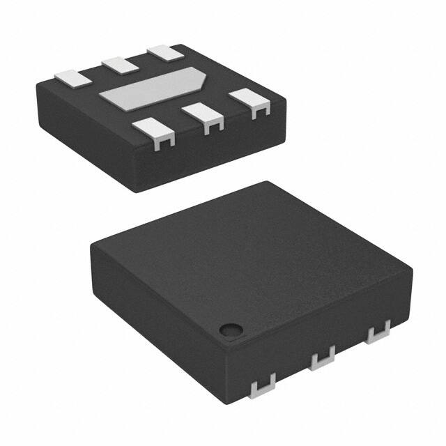
The ISL28290 is available in the 10 Ld UTQFN
(1.8mmx1.4mm), 10 Ld MSOP and 8 LD SOIC
packages. Device operation is guaranteed over
−40°C to +125°C.
Related Information
Features
▪ 1nV/√Hz input voltage noise
▪ 1kHz THD+N typical 0.00017% at 2VP−P VOUT
▪ Harmonic Distortion −87dBc, −90dBc, fO = 1MHz
▪ 170MHz −3dB bandwidth
▪ 50V/µs slew rate
▪ 700µV maximum offset voltage
▪ 10µA typical input bias current
▪ 103dB typical CMRR
▪ 3V to 5.5V single supply voltage range
▪ Rail-to-rail output
▪ Ground sensing
For a full list of related documents, visit our website:
▪ Enable pin (not available in the 8 Ld SOIC
package option)
▪ ISL28290 device page
▪ Pb-free (RoHS compliant)
Applications
▪ Low noise signal processing
▪ Low noise microphones/preamplifiers
▪ ADC buffers
▪ DAC output amplifiers
▪ Digital scales
▪ Strain gauges/sensor amplifiers
▪ Radio systems
▪ Portable equipment
▪ Infrared detectors
FN6247 Rev.12.0
Jan.12.21
Page 1
�ISL28290 Datasheet
Contents
1.
Overview . . . . . . . . . . . . . . . . . . . . . . . . . . . . . . . . . . . . . . . . . . . . . . . . . . . . . . . . . . . . . . . . . . . . . . . . . . . 3
1.1
2.
Pin Information . . . . . . . . . . . . . . . . . . . . . . . . . . . . . . . . . . . . . . . . . . . . . . . . . . . . . . . . . . . . . . . . . . . . . . 4
2.1
2.2
3.
Ordering Information . . . . . . . . . . . . . . . . . . . . . . . . . . . . . . . . . . . . . . . . . . . . . . . . . . . . . . . . . . . . . . 3
Pin Configuration . . . . . . . . . . . . . . . . . . . . . . . . . . . . . . . . . . . . . . . . . . . . . . . . . . . . . . . . . . . . . . . . . 4
Pin Descriptions . . . . . . . . . . . . . . . . . . . . . . . . . . . . . . . . . . . . . . . . . . . . . . . . . . . . . . . . . . . . . . . . . 4
Specifications . . . . . . . . . . . . . . . . . . . . . . . . . . . . . . . . . . . . . . . . . . . . . . . . . . . . . . . . . . . . . . . . . . . . . . . 6
3.1
3.2
3.3
3.4
Absolute Maximum Ratings . . . . . . . . . . . . . . . . . . . . . . . . . . . . . . . . . . . . . . . . . . . . . . . . . . . . . . . . .
Thermal Information . . . . . . . . . . . . . . . . . . . . . . . . . . . . . . . . . . . . . . . . . . . . . . . . . . . . . . . . . . . . . .
Recommended Operation Conditions . . . . . . . . . . . . . . . . . . . . . . . . . . . . . . . . . . . . . . . . . . . . . . . . .
Electrical Specifications . . . . . . . . . . . . . . . . . . . . . . . . . . . . . . . . . . . . . . . . . . . . . . . . . . . . . . . . . . . .
6
6
6
7
4.
Typical Performance Curves . . . . . . . . . . . . . . . . . . . . . . . . . . . . . . . . . . . . . . . . . . . . . . . . . . . . . . . . . . 10
5.
Applications Information . . . . . . . . . . . . . . . . . . . . . . . . . . . . . . . . . . . . . . . . . . . . . . . . . . . . . . . . . . . . . 15
5.1
5.2
5.3
5.4
5.5
5.6
5.7
Product Description . . . . . . . . . . . . . . . . . . . . . . . . . . . . . . . . . . . . . . . . . . . . . . . . . . . . . . . . . . . . . .
Enable/Power-Down . . . . . . . . . . . . . . . . . . . . . . . . . . . . . . . . . . . . . . . . . . . . . . . . . . . . . . . . . . . . .
Input Protection . . . . . . . . . . . . . . . . . . . . . . . . . . . . . . . . . . . . . . . . . . . . . . . . . . . . . . . . . . . . . . . . .
Using Only One Channel . . . . . . . . . . . . . . . . . . . . . . . . . . . . . . . . . . . . . . . . . . . . . . . . . . . . . . . . . .
Power Supply Bypassing and Printed Circuit Board Layout . . . . . . . . . . . . . . . . . . . . . . . . . . . . . . .
Current Limiting . . . . . . . . . . . . . . . . . . . . . . . . . . . . . . . . . . . . . . . . . . . . . . . . . . . . . . . . . . . . . . . . .
Power Dissipation . . . . . . . . . . . . . . . . . . . . . . . . . . . . . . . . . . . . . . . . . . . . . . . . . . . . . . . . . . . . . . .
15
15
15
15
16
16
16
6.
Revision History . . . . . . . . . . . . . . . . . . . . . . . . . . . . . . . . . . . . . . . . . . . . . . . . . . . . . . . . . . . . . . . . . . . . 17
7.
Package Outline Drawings . . . . . . . . . . . . . . . . . . . . . . . . . . . . . . . . . . . . . . . . . . . . . . . . . . . . . . . . . . . . 18
FN6247 Rev.12.0
Jan.25.21
Page 2
�ISL28290 Datasheet
1. Overview
1.1
Ordering Information
Part[1]
Marking
Part Number
Temp Range (°C)
ISL28290FUZ
8290Z
−40 to +125
ISL28290FUZ-T7
8290Z
−40 to +125
ISL28290FRUZ-T7
E
−40 to +125
ISL28290FBZ
28290 FBZ
−40 to +125
ISL28290FBZ-T7
28290 FBZ
−40 to +125
ISL28290EVAL1Z
Evaluation Board
1.
The part marking is located on the bottom of the part.
2.
See TB347 for details about reel specifications.
FN6247 Rev.12.0
Jan.25.21
Tape and Reel[2]
(Units)
Package
(RoHS Compliant)
Pkg. Dwg. #
10 Ld MSOP
M10.118A
1.5k
10 Ld MSOP
M10.118A
3k
10 Ld UTQFN
L10.1.8x1.4A
8 Ld SOIC
M8.15E
8 Ld SOIC
M8.15E
1k
Page 3
�ISL28290 Datasheet
2. Pin Information
Pin Configuration
+
V- 4
ENABLE_A 5
7 IN+_B
IN-_A
OUT_B
8 IN-_B
10
9
8
1
7
6 ENABLE_B
IN+_A
IN-_B
+
+
6 IN+_B
2
3
4
5
ENABLE_B
IN+_A 3
9 OUT_B
+
ENABLE_A
IN-_A 2
10 V+
V+
OUT_A 1
ISL28290
(10 Ld UTQFN)
Top View
OUT_A
ISL28290
(10 Ld MSOP)
Top View
V-
2.1
ISL28290
(8 Ld SOIC)
Top View
OUT_A 1
IN-_A 2
IN+_A 3
8 V+
+
V- 4
2.2
7 OUT_B
+
6 IN-_B
5 IN+_B
Pin Descriptions
ISL28290
ISL28290
ISL28290
Pin
(10 Ld MSOP)
(10 Ld UTQFN)
(8 Ld SOIC)
Name
Function
Equivalent
1 (A)
7 (B)
2 (A)
6 (B)
IN−
IN−_A
IN−_B
Inverting input
2 (A)
8 (B)
Circuit
V+
IN-
IN+
V-
Circuit 1
2 (A)
6 (B)
3 (A)
5 (B)
IN+
IN+_A
IN+_B
Non-inverting input
3 (A)
7 (B)
4
3
4
V−
Negative supply
FN6247 Rev.12.0
Jan.25.21
(See Circuit 1)
Page 4
�ISL28290 Datasheet
ISL28290
ISL28290
ISL28290
Pin
Equivalent
(10 Ld MSOP)
(10 Ld UTQFN)
(8 Ld SOIC)
Name
Function
10 (A)
8 (B)
1 (A)
7 (B)
OUT
OUT_A
OUT_B
Output
1 (A)
9 (B)
Circuit
V+
OUT
V-
Circuit 2
10
9
5 (A)
6 (B)
4 (A)
5 (B)
8
V+
Positive supply
N/A
EN
EN_A
EN_B
Enable BAR pin
internal pull-down;
Logic “1” selects the
disabled state;
Logic “0” selects the
enabled state.
V+
EN
V-
Circuit 3
FN6247 Rev.12.0
Jan.25.21
Page 5
�ISL28290 Datasheet
3. Specifications
3.1
Absolute Maximum Ratings
Parameter
Minimum
Maximum
Unit
5.5
mA
Supply Turn-On Voltage Slew Rate
1
V/µs
Differential Input Current
5
mA
Differential Input Voltage
0.5
V
V+ + 0.5
V
Supply Voltage
Input Voltage
V- − 0.5
ESD Rating
Value
Unit
3
kV
Machine Model
300
V
Charged Device Model (Tested per JS-002-2014)
1200
V
Human Body Model (Tested per JS-001-2017)
CAUTION: Do not operate at or near the maximum ratings listed for extended periods of time. Exposure to such conditions
can adversely impact product reliability and result in failures not covered by warranty.
3.2
Thermal Information
Thermal Resistance (Typical)[1] [2] [3] [4]
θJA (°C/W)
θJC (°C/W)
8 Ld SOIC Package
110
82
10 Ld MSOP Package
175
90
10 Ld UTQFN Package
190
140
1.
θJA is measured with the component mounted on a high effective thermal conductivity test board in free air. See Tech Brief TB379
for details.
2.
θJA is measured in free air with the component mounted on a high effective thermal conductivity test board with direct attach
features. See Tech Brief TB379.
3.
For θJC, the case temperature location is the center of the exposed metal pad on the package underside.
4.
For θJC, the case temperature location is taken at the package top center.
Parameter
Minimum
Maximum Junction Temperature
Maximum Storage Temperature Range
−65
Pb-Free Reflow Profile
3.3
Maximum
Unit
+125
°C
+150
°C
see TB493
Recommended Operation Conditions
Parameter
Minimum
Supply Voltage
Ambient Temperature
FN6247 Rev.12.0
Jan.25.21
−40
Maximum
Unit
5.0
V
+125
°C
Page 6
�ISL28290 Datasheet
3.4
Electrical Specifications
V+ = 5.0V, V− = GND, RL = Open, RF = 1kΩ, AV = −1 unless otherwise specified. Parameters are per amplifier. Typical
values are at V+ = 5V, TA = +25°C. Boldface limits apply over the operating temperature range, −40°C to
+125°C, temperature data established by characterization.
Parameter
Symbol
Test Conditions
Min[1]
Typ
Max[1]
Unit
−1100
240
700
µV
DC Specifications
Input Offset Voltage
VOS
900
Input Offset Drift vs
Temperature
ΔV OS
--------------ΔT
Input Offset Current
IIO
See Figure 21
1.9
40
µV⁄°C
500
nA
900
Input Bias Current
IB
10
16
µA
18
Common-Mode Voltage
Range
VCM
0
3.8
V
Common-Mode Rejection
Ratio
CMRR
VCM = 0V to 3.8V
78
103
dB
Power Supply Rejection
Ratio
PSRR
VS = 3V to 5V
74
80
dB
Large Signal Voltage Gain
AVOL
VO = 0.5V to 4V, RL = 1kΩ
94
102
dB
90
Maximum Output Voltage
Swing
VOUT
Output low, RL = 1kΩ
20
50
mV
80
Output high, RL = 1kΩ, V+ = 5V
4.95
4.97
V
4.92
Supply Current per Channel,
Enabled
IS,ON
Supply Current, Disabled
IS,OFF
8.5
11
mA
13
26
35
µA
52
Short-Circuit Output Current
IO+
RL = 10Ω
95
144
mA
90
FN6247 Rev.12.0
Jan.25.21
Page 7
�ISL28290 Datasheet
V+ = 5.0V, V− = GND, RL = Open, RF = 1kΩ, AV = −1 unless otherwise specified. Parameters are per amplifier. Typical
values are at V+ = 5V, TA = +25°C. Boldface limits apply over the operating temperature range, −40°C to
+125°C, temperature data established by characterization.(Cont.)
Parameter
Symbol
Short-Circuit Output Current
IO−
Test Conditions
RL = 10Ω
Min[1]
Typ
95
135
Max[1]
Unit
mA
90
Supply Operating Range
VSUPPLY
V+ to V−
3
2
EN High Level
VENH
Referred to V−
EN Low Level
VENL
Referred to V−
EN Pin Input High Current
IENH
VEN = V+
5.5
V
V
0.8
0.8
V
1.2
µA
1.4
EN Pin Input Low Current
IENL
VEN = V−
20
80
nA
100
AC Specifications
−3dB Unity Gain Bandwidth
GBW
Total Harmonic Distortion +
Noise
THD+N
f = 1kHz, VOUT + 2VP−P, AV = +1, RL = 10kΩ
2nd Harmonic Distortion
HD
(1MHz)
VOUT = 2VP−P, AV = 1
3rd Harmonic Distortion
Off-state Isolation
fO = 100kHz
Channel-to-Channel
Crosstalk
fO = 100kHz
ISO
X-TALK
RF = 0Ω CL = 20pF, AV = 1, RL = 10kΩ
170
MHz
0.000
17
%
−87
dBc
−90
dBc
AV = +1; VIN = 100mVP−P; RF = 0Ω,
CL = 20pF,
AV = 1, RL = 10kΩ
−38
dB
VS = ±2.5V; AV = +1; VIN = 1VP−P, RF = 0Ω,
CL = 20pF, AV = 1, RL = 10kΩ
−105
dB
Power Supply Rejection
Ratio
fO = 100kHz
PSRR
VS = ±2.5V; AV = +1; VSOURCE = 1VP−P,
RF = 0Ω,
CL = 20pF, AV = 1, RL = 10kΩ
−70
dB
Common Mode Rejection
Ratio
fO = 100kHz
CMRR
VS = ±2.5V; AV = +1; VCM = 1VP−P, RF = 0Ω,
CL = 20pF, AV = 1, RL = 10kΩ
−65
dB
Input Referred Voltage Noise
en
fO = 1kHz
1
nV/√Hz
Input Referred Current Noise
in
fO = 10kHz
2.1
pA/√Hz
50
V/µs
1.0
ns
3.3
ns
6.3
ns
Transient Response
Slew Rate
SR
30
25
Propagation Delay
10% VIN − 10% VOUT
Rise Time, tr 10% to 90%
Fall Time, tf 10% to 90%
FN6247 Rev.12.0
Jan.25.21
tpd
AV = 1, VOUT = 100mVP−P, RF = 0Ω,
CL = 1.2pF
tr, tf, Small AV = +1, VOUT = 0.1VP−P, RF = 0Ω,
Signal
CL = 1.2pF
Page 8
�ISL28290 Datasheet
V+ = 5.0V, V− = GND, RL = Open, RF = 1kΩ, AV = −1 unless otherwise specified. Parameters are per amplifier. Typical
values are at V+ = 5V, TA = +25°C. Boldface limits apply over the operating temperature range, −40°C to
+125°C, temperature data established by characterization.(Cont.)
Parameter
Rise Time, tr 10% to 90%
Fall Time, tf 10% to 90%
Symbol
tr, tf Large
Signal
Rise Time, tr 10% to 90%
Fall Time, tf 10% to 90%
Settling Time to 0.1%
90% VOUT to 0.1% VOUT
ENABLE to Output Turn-on
Delay Time; 10% EN − 10%
VOUT
ENABLE to Output Turn-off
Delay Time; 10% EN − 10%
VOUT
1.
ts
tEN
Test Conditions
Min[1]
Typ
Max[1]
Unit
AV = +2, VOUT = 1VP−P, RF = RG = 499Ω,
RL = 10kΩ,
CL = 1.2pF
44
ns
51
ns
AV = +2, VOUT = 4.7VP−P, RF = RG = 499Ω,
RL = 10kΩ, CL = 1.2pF
190
ns
187
ns
AV = 1, VOUT = 1VP−P, RF = 0Ω, CL = 1.2pF
45
ns
AV = 1, VOUT = 1VDC, RL = 10kΩ, CL = 1.2pF
330
ns
AV = 1, VOUT = 0VDC, RL = 10kΩ, CL = 1.2pF
50
ns
Compliance to datasheet limits is assured by one or more methods: production test, characterization and/or design.
FN6247 Rev.12.0
Jan.25.21
Page 9
�ISL28290 Datasheet
4. Typical Performance Curves
2
0
RL = 10k
-1
CLOSED LOOP GAIN (dB)
CLOSED LOOP GAIN (dB)
10
RL = 100k
1
RL = 100
-2
-3
-4
RL = 1k
-5
V+ = 5V
-6 AV = +1
C = 10pF
-7 V L = 10mV
OUT
P-P
-8
100k
1M
100M
10M
CL = 92pF
CL = 57pF
CL = 32pF
0
CL = 20pF
-2
-4
V+ = 5V
-6 AV = +1
R = 10kΩ
-8 V L = 10mV
OUT
P-P
-10
10k
100k
0
VOUT = 1VP-P
-2
VOUT = 100mVP-P
-4
V+ = 5V
AV = +1
RL = 10kΩ
CL = 10pF
-6
-7
-8
10k
VOUT = 10mVP-P
1M
10M
10
100M
AV = 1, RF = 0, RG = INF
-10
10k
1G
100k
1M
10M
100M
FREQUENCY (Hz)
Figure 3. -3dB Bandwidth vs VOUT
Figure 4. Frequency Response vs Closed Loop Gain
1M
1M
100k
OUTPUT IMPEDANCE (Ω)
INPUT IMPEDANCE (Ω)
VOUT = 100mVP-P
AV = 10, RF = 4.42k, RG = 499
FREQUENCY (Hz)
10k
1k
100
1G
30
0
100k
100M
AV = 1000, RF = 499k, RG = 499 V+ = 5V
RL = 10k
50 AV = 100,
RF = 49.9k, RG = 499
40
20
-5
10M
70
60
-3
1M
Figure 2. Gain vs Frequency For Various CLOAD
VOUT = 1mVP-P
-1
CL = 1pF
FREQUENCY (Hz)
GAIN (dB)
CLOSED LOOP GAIN (dB)
6
2
1G
Figure 1. Gain vs Frequency For Various RLOAD
1
CL = 110pF
4
FREQUENCY (Hz)
2
8
V+ = 5V, 3V
ENABLED AND
DISABLED
VSOURCE = 1VP-P
10
100k
1M
10M
100M
FREQUENCY (Hz)
Figure 5. Input Impedance vs Frequency
FN6247 Rev.12.0
Jan.25.21
1G
100k
10k
1k
100
V+ = 5V, 3V
VSOURCE = 1VP-P
10
100k
1M
10M
100M
1G
FREQUENCY (Hz)
Figure 6. Disabled Output Impedance vs Frequency
Page 10
�ISL28290 Datasheet
0
100
-10
-20
10
-30
CMRR (dB)
OUTPUT IMPEDANCE (Ω)
V+ = 5V, 3V
1
-40
-50
-60
-70
V+ = 5V
AV = +1
RL = 10kΩ
CL = 10pF
VCM = 100mVP-P
-80
0.1
-90
-100
0.01
100k
1M
10M
100M
-110
1k
1G
10k
100k
FREQUENCY (Hz)
Figure 7. Enabled Output Impedance vs Frequency
-10
-20
PSRR (dB)
-30
V+ = 5V
AV = +1
RL = 10kΩ
CL = 10pF
VSOURCE = 100mVP-P
-10
PSRR+
-50
-60
-70
VP-P = 100mV
-30
-40
-50
-60
100k
1M
FREQUENCY (Hz)
10M
VP-P = 10mV
-80
10k
100M
Figure 9. PSRR vs Frequency
100k
1M
10M
FREQUENCY (Hz)
100M
1G
Figure 10. Off Isolation vs Frequency
0.1
-20
V+ = 5V
RL = 10k
-30
THD + NOISE (%)
-40
CROSSTALK (dB)
V+ = 5V
AV = +1
RL = 10kΩ
CL = 10pF
-70
-80
10k
100M
VP-P = 1V
-20
PSRR-
-40
-90
1k
10M
Figure 8. CMRR vs Frequency
OFF ISOLATION (dB)
0
1M
FREQUENCY (Hz)
-50
-60
-70
VP-P = 1V
-80
-90
RF = 0, AV = 1
VOUT = 2VP-P
400Hz TO 22kHz FILTER
0.01
0.001
-100
-110
-120
10k
100k
1M
10M
FREQUENCY (Hz)
100M
1G
Figure 11. Channel-To-Channel Crosstalk vs Frequency
FN6247 Rev.12.0
Jan.25.21
0.0001
0
2k
4k
6k
8k 10k 12k 14k 16k 18k 20k
FREQUENCY (Hz)
Figure 12. THD+N vs Frequency
Page 11
�ISL28290 Datasheet
10
V+ = 5V
RL = 10k
RF = 0, AV = 1
FREQUENCY= 1kHz
400Hz TO 22kHz FILTER
1
THD + NOISE (%)
INPUT VOLTAGE NOISE (nV/√Hz)
10
0.1
0.01
0.001
0.0001
0
0.5
1.0
1.5
2.0
2.5
3.0
3.5
1
0.1
0.1
4.0
1
10
VOUT (VP-P)
Figure 13. THD+N at 1kHz vs VOUT
1k
10k
100k
Figure 14. Input Referred Noise Voltage vs Frequency
1000
5
V+ = 5V
AV = +1
RL = 10kΩ
CL = 10pF
VIN = 1VDC
EN INPUT
4
100
VOLTS (V)
CURRENT NOISE (pA/√Hz)
100
FREQUENCY (Hz)
3
2
ENABLE
10
DISABLE
ENABLE
1
OUTPUT
1
0.1
1
10
100
1k
10k
0
100k
-1
0
1
FREQUENCY (Hz)
0.08
0.8
0.06
0.6
VOUT
0.02
VIN
0
-0.02
V+ = ±2.5V
AV = +1
RL = 10kΩ
VOUT = 100mVP-P
-0.04
-0.06
-0.08
0
20
40
60
80
100 120 140 160 180 200
TIME (ns)
Figure 17. Small Signal Step Response
FN6247 Rev.12.0
Jan.25.21
4
3
Figure 16. Enable/Disable Timing
LARGE SIGNAL (V)
SMALL SIGNAL (V)
Figure 15. Input Referred Noise Current vs Frequency
0.04
2
TIME (µs)
VOUT
0.4
VIN
0.2
0
-0.2
V+ = ±2.5V
AV = +2
RF = RG = 499Ω
RL = 10kΩ
VOUT = 1VP-P
-0.4
-0.6
-0.8
0
100
200
300
400 500
TIME (ns)
600
700
800
Figure 18. Large Signal (1V) Step Response
Page 12
�ISL28290 Datasheet
3
6.0
VOUT
2
MAX
1
0
V+ = ±2.5V
AV = +2
RF = RG = 499Ω
RL = 10kΩ
VOUT = 4.7VP-P
-1
-2
0
400
800
5.0
CURRENT (mA)
LARGE SIGNAL (V)
VIN
-3
n = 50
5.5
MEDIAN
4.5
4.0
MIN
3.5
3.0
1200
1600
2.5
-40
2000
-20
0
TIME (ns)
Figure 19. Large Signal (4.7V) Step Response
600
500
-9
120
n = 50
-10
MAX
MAX
300
200
-11
MEDIAN
IBIAS+ (µA)
VOS (µV)
100
Figure 20. Supply Current vs Temperature,
VS = ±2.5V Enabled, RL = INF
n = 50
400
20
40
60
80
TEMPERATURE (°C)
100
0
-100
-12
MEDIAN
-13
-200
MIN
MIN
-300
-14
-400
-500
-40
-20
0
20
40
60
80
100
-15
-40
120
-20
0
Figure 21. VOS vs Temperature VS = ±2.5V
800
80
100
120
n = 50
600
MAX
-11
400
IIO (nA)
IBIAS- (µA)
60
Figure 22. IBIAS+ vs Temperature VS = ±2.5V
n = 50
-10
40
TEMPERATURE (°C)
TEMPERATURE (°C)
-9
20
MEDIAN
-12
-13
MAX
200
0 MEDIAN
MIN
-14
-200
-15
-40
-400
-40
MIN
-20
0
20
40
60
80
TEMPERATURE (°C)
100
120
Figure 23. IBIAS- vs Temperature VS = ±2.5V
FN6247 Rev.12.0
Jan.25.21
-20
0
20
40
60
80
100
120
TEMPERATURE (°C)
Figure 24. IIO vs Temperature VS = ±2.5V
Page 13
�ISL28290 Datasheet
140
83
n = 50
MAX
130
MEDIAN
81
PSRR (dB)
CMRR (dB)
120
110
100
MIN
90
80
79
MEDIAN
78
MIN
76
-40
-20
0
20
40
60
80
TEMPERATURE (°C)
100
4.982
75
-40
120
50
MAX
40
60
80
100
120
n = 50
40
4.976
VOUT (mV)
4.974
MEDIAN
4.970
MIN
4.968
MAX
35
30
MEDIAN
25
MIN
20
4.966
15
4.964
4.962
-40
20
45
4.978
4.972
0
Figure 26. PSRR vs Temperature ±1.5V to ±2.5V
n = 50
4.980
-20
TEMPERATURE (°C)
Figure 25. CMRR vs Temperature,
VCM = 3.8V, VS = ±2.5V
VOUT (V)
MAX
77
80
70
n = 50
82
-20
0
20
40
60
80
100
120
10
-40
-20
0
Figure 27. Positive VOUT vs Temperature RL = 1k,
VS = ±2.5V
VCM OVERHEAD TO SUPPLY RAILS (V)
20
40
60
80
100
120
TEMPERATURE (°C)
TEMPERATURE (°C)
Figure 28. Negative VOUT vs Temperature RL = 1k,
VS = ±2.5V
1.2
1.0
0.8
INPUT VOLTAGE TO THE POSITIVE RAIL (V+ - VCM)
0.6
0.4
0.2
0
-0.2
-0.4
-0.6
-0.8
-60
INPUT VOLTAGE TO THE NEGATIVE RAIL (V- + VCM)
-40
-20
0
20 40 60 80
TEMPERATURE (°C)
100 120 140
Figure 29. Input Common Mode Voltage vs Temperature
FN6247 Rev.12.0
Jan.25.21
Page 14
�ISL28290 Datasheet
5. Applications Information
5.1
Product Description
The ISL28290 is a voltage feedback operational amplifier designed for communication and imaging applications
requiring low distortion, very low voltage and current noise. The part features high bandwidth while drawing
moderately low supply current. The ISL28290 uses a classical voltage-feedback topology, which allows it to be
used in a variety of applications where current-feedback amplifiers are not appropriate because of restrictions
placed upon the feedback element used with the amplifier.
5.2
Enable/Power-Down
The ISL28290 amplifier is disabled by applying a voltage greater than 2V to the EN pin, with respect to the V- pin.
In this condition, the output(s) will be in a high impedance state and the amplifier current will be reduced to
13µA ⁄Amp. By disabling the part, multiple parts can be connected together as a MUX. The outputs are tied
together in parallel and a channel can be selected by the EN pin. The EN pin also has an internal pull-down. If left
open, the EN pin will pull to the negative rail and the device will be enabled by default.
5.3
Input Protection
All input terminals have internal ESD protection diodes to both positive and negative supply rails, limiting the input
voltage to within one diode beyond the supply rails. The device has additional back-to-back diodes across the
input terminals (as shown in Figure 30). In pulse applications where the input Slew Rate exceeds the Slew Rate of
the amplifier, the possibility exists for the input protection diodes to become forward biased. This can cause
excessive input current and distortion at the outputs. If overdriving the inputs is necessary, the external input
current must never exceed 5mA. An external series resistor may be used to limit the current, as shown
in Figure 30.
+
Figure 30. Limiting the Input Current to Less Than 5mA
5.4
Using Only One Channel
The ISL28290 is a Dual channel op amp. If the application only requires one channel when using the ISL28290,
the user must configure the unused channel to prevent it from oscillating. Oscillation can occur if the input and
output pins are floating. This will result in higher than expected supply currents and possible noise injection into
the channel being used. The proper way to prevent this oscillation is to short the output to the negative input and
ground the positive input (as shown in Figure 31).
+
Figure 31. Preventing Oscillations in Unused Channels
FN6247 Rev.12.0
Jan.25.21
Page 15
�ISL28290 Datasheet
5.5
Power Supply Bypassing and Printed Circuit Board Layout
As with any high frequency device, good printed circuit board layout is necessary for optimum performance. Low
impedance ground plane construction is essential. Surface mount components are recommended, but if leaded
components are used, lead lengths should be as short as possible. The power supply pins must be well bypassed
to reduce the risk of oscillation. The combination of a 4.7µF tantalum capacitor in parallel with a 0.01µF capacitor
has been shown to work well when placed at each supply pin.
For good AC performance, parasitic capacitance should be kept to a minimum, especially at the inverting input.
When ground plane construction is used, it should be removed from the area near the inverting input to minimize
any stray capacitance at that node. Carbon or Metal-Film resistors are acceptable with the Metal-Film resistors
giving slightly less peaking and bandwidth because of additional series inductance. Use of sockets, particularly for
the SO package, should be avoided if possible. Sockets add parasitic inductance and capacitance, which will
result in additional peaking and overshoot.
5.6
Current Limiting
The ISL28290 has no internal current-limiting circuitry. If the output is shorted, it is possible to exceed the Absolute
Maximum Rating for output current or power dissipation, potentially resulting in the destruction of the device. This
is why output short circuit current is specified and tested with RL = 10Ω.
5.7
Power Dissipation
It is possible to exceed the +125°C maximum junction temperatures under certain load and power-supply
conditions. It is therefore important to calculate the maximum junction temperature (TJMAX) for all applications to
determine if power supply voltages, load conditions, or package type need to be modified to remain in the safe
operating area. These parameters are related as follows:
(EQ. 1)
T JMAX = T MAX + ( θ JA xPD MAXTOTAL )
where:
▪ PDMAXTOTAL is the sum of the maximum power dissipation of each amplifier in the package (PDMAX)
▪ PDMAX for each amplifier can be calculated as follows:
(EQ. 2)
V OUTMAX
PD MAX = 2*V S × I SMAX + ( V S - V OUTMAX ) × ---------------------------RL
▪ where TMAX = Maximum ambient temperature
▪ θJA = Thermal resistance of the package
▪ PDMAX = Maximum power dissipation of 1 amplifier
▪ VS = Supply voltage
▪ IMAX = Maximum supply current of 1 amplifier
▪ VOUTMAX = Maximum output voltage swing of the application
▪ RL = Load resistance
FN6247 Rev.12.0
Jan.25.21
Page 16
�ISL28290 Datasheet
6. Revision History
Rev.
Description
12.00
Jan.12.21
FN6247 Rev.12.0
Jan.25.21
Description
Datasheet formatting overhaul.
Removed all references to ISL28190.
Page 17
�ISL28290 Datasheet
7. Package Outline Drawings
L10.1.8x1.4A
10 Lead Ultra Thin Quad Flat No-lead Plastic Package
Rev 6, 8/13
1.80
B
C0.10
IN #1 ID
6
A
1
1
1.40
3
10
0.50
6 PIN 1
INDEX AREA
9 X 0.40
2
10X 0.20 4
0.10 M C A B
0.05 M C
0.70
8
5
0.10
7
2X
4X 0.30
6
6X 0.40
TOP VIEW
BOTTOM VIEW
SEE DETAIL "X"
0.10 C
MAX. 0.55
2.20
1
3
10
(0.70)
SIDE VIEW
1.80
(10X 0.20)
C
SEATING PLANE
0.08 C
8
C
5
(9X 0.60)
6
0.127 REF
7
(6X 0.40)
PACKAGE OUTLINE
0-0.05
TYPICAL RECOMMENDED LAND PATTERN
DETAIL "X"
NOTES:
1.
Dimensions are in millimeters.
Dimensions in ( ) for Reference Only.
2.
Dimensioning and tolerancing conform to ASME Y14.5m-1994.
3.
Unless otherwise specified, tolerance : Decimal ± 0.05
4.
Lead width dimension applies to the metallized terminal and is
measured between 0.15mm and 0.30mm from the terminal tip.
5.
JEDEC reference MO-255.
6.
The configuration of the pin #1 identifier is optional, but must be
located within the zone indicated. The pin #1 identifier may be
either a mold or mark feature.
FN6247 Rev.12.0
Jan.25.21
Page 18
�ISL28290 Datasheet
M8.15E
8 Lead Narrow Body Small Outline Plastic Package
Rev 0, 08/09
4
4.90 ± 0.10
A
DETAIL "A"
0.22 ± 0.03
B
6.0 ± 0.20
3.90 ± 0.10
4
PIN NO.1
ID MARK
5
(0.35) x 45°
4° ± 4°
0.43 ± 0.076
1.27
0.25 M C A B
SIDE VIEW “B”
TOP VIEW
1.75 MAX
1.45 ± 0.1
0.25
GAUGE PLANE
C
SEATING PLANE
0.10 C
0.175 ± 0.075
SIDE VIEW “A
0.63 ±0.23
DETAIL "A"
(1.27)
(0.60)
NOTES:
(1.50)
(5.40)
1.
Dimensions are in millimeters.
Dimensions in ( ) for Reference Only.
2.
Dimensioning and tolerancing conform to AMSE Y14.5m-1994.
3.
Unless otherwise specified, tolerance : Decimal ± 0.05
4.
Dimension does not include interlead flash or protrusions.
Interlead flash or protrusions shall not exceed 0.25mm per side.
5.
The pin #1 identifier may be either a mold or mark feature.
6.
Reference to JEDEC MS-012.
TYPICAL RECOMMENDED LAND PATTERN
FN6247 Rev.12.0
Jan.25.21
Page 19
�ISL28290 Datasheet
M10.118A (JEDEC MO-187-BA)
10 Lead Mini Small Outline Plastic Package (MSOP)
Rev 0, 9/09
3.0 ± 0.1
A
0.25
10
DETAIL "X"
CAB
0.18 ± 0.05
SIDE VIEW 2
4.9 ± 0.15
3.0 ± 0.1
1.10 Max
B
PIN# 1 ID
1
2
0.95 BSC
0.5 BSC
TOP VIEW
Gauge
Plane
0.86 ± 0.09
H
0.25
C
3°±3°
SEATING PLANE
0.10 ± 0.05
0.23 +0.07/ -0.08
0.08 C AB
0.55 ± 0.15
0.10 C
DETAIL "X"
SIDE VIEW 1
5.80
4.40
3.00
NOTES:
0.50
0.30
1.
Dimensions are in millimeters.
2.
Dimensioning and tolerancing conform to AMSE Y14.5m-1994.
3.
Plastic or metal protrusions of 0.15mm max per side are not
included.
Plastic interlead protrusions of 0.25mm max per side are not
included.
4.
1.40
5.
Dimensions “D” and “E1” are measured at Datum Plane “H”.
TYPICAL RECOMMENDED LAND PATTERN
6.
This replaces existing drawing # MDP0043 MSOP10L.
FN6247 Rev.12.0
Jan.25.21
Page 20
�IMPORTANT NOTICE AND DISCLAIMER
RENESAS ELECTRONICS CORPORATION AND ITS SUBSIDIARIES (“RENESAS”) PROVIDES TECHNICAL
SPECIFICATIONS AND RELIABILITY DATA (INCLUDING DATASHEETS), DESIGN RESOURCES (INCLUDING
REFERENCE DESIGNS), APPLICATION OR OTHER DESIGN ADVICE, WEB TOOLS, SAFETY INFORMATION, AND
OTHER RESOURCES “AS IS” AND WITH ALL FAULTS, AND DISCLAIMS ALL WARRANTIES, EXPRESS OR IMPLIED,
INCLUDING, WITHOUT LIMITATION, ANY IMPLIED WARRANTIES OF MERCHANTABILITY, FITNESS FOR A
PARTICULAR PURPOSE, OR NON-INFRINGEMENT OF THIRD PARTY INTELLECTUAL PROPERTY RIGHTS.
These resources are intended for developers skilled in the art designing with Renesas products. You are solely responsible
for (1) selecting the appropriate products for your application, (2) designing, validating, and testing your application, and (3)
ensuring your application meets applicable standards, and any other safety, security, or other requirements. These
resources are subject to change without notice. Renesas grants you permission to use these resources only for
development of an application that uses Renesas products. Other reproduction or use of these resources is strictly
prohibited. No license is granted to any other Renesas intellectual property or to any third party intellectual property.
Renesas disclaims responsibility for, and you will fully indemnify Renesas and its representatives against, any claims,
damages, costs, losses, or liabilities arising out of your use of these resources. Renesas' products are provided only subject
to Renesas' Terms and Conditions of Sale or other applicable terms agreed to in writing. No use of any Renesas resources
expands or otherwise alters any applicable warranties or warranty disclaimers for these products.
(Rev.1.0 Mar 2020)
Corporate Headquarters
Contact Information
TOYOSU FORESIA, 3-2-24 Toyosu,
Koto-ku, Tokyo 135-0061, Japan
www.renesas.com
For further information on a product, technology, the most
up-to-date version of a document, or your nearest sales
office, please visit:
www.renesas.com/contact/
Trademarks
Renesas and the Renesas logo are trademarks of Renesas
Electronics Corporation. All trademarks and registered
trademarks are the property of their respective owners.
© 2021 Renesas Electronics Corporation. All rights reserved.
�


 工商网监
湘ICP备2023018690号
工商网监
湘ICP备2023018690号
