Dual Micropower, Zero-Drift, RRIO Operational
Amplifiers
ISL28233I
Features
The ISL28233IUZ is a dual micropower, zero-drift
operational amplifier that is optimized for single and dual
supply operation from 1.65V to 5.5V and ±0.825V to
±2.75V. The low supply current of 18µA and wide input
range enable the ISL28233IUZ to be an excellent general
purpose op amp for a range of applications. The
ISL28233IUZ is ideal for handheld devices that operate
off 2 AA or single Li-ion batteries.
• Low Input Offset Voltage . . . . . . . . . . . 8µV, Max.
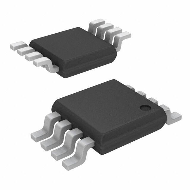
The ISL28233IUZ is available in an industry standard
pinout 8 Ld MSOP package. It operates over the
temperature range of -40°C to +85°C.
• Input Bias Current . . . . . . . . . . . . . 110pA, Max.
• Low Offset Drift . . . . . . . . . . . . . 0.06µV/°C, Max
• Quiescent Current (Per Amplifier) . . . . . 18µA, Typ.
• Single Supply Range . . . . . . . . . +1.65V to +5.5V
• Dual Supply Range . . . . . . . . ±0.825V to ±2.75V
• Low Noise (0.01Hz to 10Hz) . . . . . . . 1.1µVP-P, Typ.
• Rail-to-Rail Inputs and Output
• Operating Temperature Range . . . -40°C to +85°C
Applications
• Bi-Directional Current Sense
• Temperature Measurement
• Medical Equipment
• Electronic Weigh Scales
• Precision/Strain Gauge Sensor
• Precision Regulation
• Low Ohmic Current Sense
• High Gain Analog Front Ends
Typical Application
VOS vs TEMP
8
6
N = 60
MAX
4
2
MEDIAN
0
-2
MIN
-4
-6
-8
-40
BI-DIRECTIONAL CURRENT SENSE AMPLIFIER
November 17, 2011
FN6942.2
1
-20
0
20
40
60
80
100
TEMPERATURE (°C)
CAUTION: These devices are sensitive to electrostatic discharge; follow proper IC Handling Procedures.
1-888-INTERSIL or 1-888-468-3774 | Copyright Intersil Americas Inc. 2010, 2011. All Rights Reserved
Intersil (and design) is a trademark owned by Intersil Corporation or one of its subsidiaries.
All other trademarks mentioned are the property of their respective owners.
�ISL28233I
Ordering Information
PART NUMBER
(Note 3)
PART MARKING
PACKAGE
(Pb-Free)
PKG.
DWG. #
ISL28233IUZ (Note 2)
8233Z
8 Ld MSOP
M8.118A
ISL28233IUZ-T7 (Notes 1, 2)
8233Z
8 Ld MSOP
M8.118A
NOTES:
1. Please refer to TB347 for details on reel specifications.
2. These Intersil Pb-free plastic packaged products employ special Pb-free material sets, molding compounds/die attach materials,
and 100% matte tin plate plus anneal (e3 termination finish, which is RoHS compliant and compatible with both SnPb and Pb-free
soldering operations). Intersil Pb-free products are MSL classified at Pb-free peak reflow temperatures that meet or exceed the
Pb-free requirements of IPC/JEDEC J STD-020.
3. For Moisture Sensitivity Level (MSL), please see device information page for ISL28233I. For more information on MSL please
see techbrief TB363.
2
FN6942.2
November 17, 2011
�ISL28233I
Pin Configurations
ISL28233IUZ
(8 LD MSOP)
TOP VIEW
OUT_A 1
IN-_A 2
8 V+
7 OUT_B
- +
IN+_A 3
+ -
V- 4
6 IN-_B
5 IN+_B
Pin Descriptions
ISL28233IUZ
(8 Ld MSOP)
PIN
NAME
FUNCTION
3
IN+_A
Non-inverting input
5
IN+_B
EQUIVALENT CIRCUIT
V+
IN+_C
+
+
IN+
IN+_D
IN-
CLOCK GEN + DRIVERS
VCircuit 1
4
V-
Negative supply
2
IN-_A
Inverting input
6
IN-_B
(See Circuit 1)
IN-_C
IN-_D
1
OUT_A
7
OUT_B
Output
V+
OUT_C
OUT
OUT_D
V-
Circuit 2
8
V+
Positive supply
3
FN6942.2
November 17, 2011
�ISL28233I
Absolute Maximum Ratings
Max Supply Voltage V+ to V- . . .
Max Voltage VIN to GND . . . . . .
Max Input Differential Voltage . .
Max Input Current . . . . . . . . . .
Max Voltage VOUT to GND (10s)
ESD Tolerance
Human Body Model . . . . . . . .
Machine Model . . . . . . . . . . .
Charged Device Model . . . . . .
Latch-Up Passed Per JESD78B . .
Thermal Information
....
(V- ....
....
....
...........
0.3V) to (V+ +
...........
...........
...........
.
.
.
.
.
.
.
.
.
.
.
.
.
.
.
.
.
.
.
.
.
.
.
.
.
.
.
.
.
.
.
.
.
.
.
.
.
.
.
.
.
.
.
.
.
.
.
.
.
.
.
.
.
.
.
.
. .6.5V
0.3V)V
. 6.5V
. 20mA
.±3.0V
. 4000V
. . 400V
. 2000V
+125°C
Thermal Resistance (Typical)
JA
(°C/W)
JC
(°C/W)
8 Ld MSOP (Notes 4, 5) . . . . . . . .
180
65
Maximum Storage Temperature Range . . . -65°C to +150°C
Pb-Free Reflow Profile . . . . . . . . . . . . . . . . . .see link below
http://www.intersil.com/pbfree/Pb-FreeReflow.asp
Operating Conditions
Temperature Range . . . . . . . . . . . . . . . . . . -40°C to +85°C
CAUTION: Do not operate at or near the maximum ratings listed for extended periods of time. Exposure to such conditions may adversely impact
product reliability and result in failures not covered by warranty.
NOTES:
4.
JA is measured with the component mounted on a high effective thermal conductivity test board in free air. See Tech Brief
TB379 for details.
5. For JC, the “case temp” location is taken at the package top center.
Electrical Specifications
PARAMETER
V+ = 5V, V- = 0V, VCM = 2.5V, TA = +25°C, RL = 10k , unless otherwise specified.
Boldface limits apply over the operating temperature range,
-40°C to +85°C.
DESCRIPTION
CONDITIONS
MIN
(Note 6)
TYP
MAX
(Note 6)
UNIT
-8
±2
8
µV
-11.9
-
11.9
µV
-0.06
0.02
0.06
µV/°C
DC SPECIFICATIONS
VOS
Input Offset Voltage
TCVOS
Input Offset Voltage Temperature
Coefficient
IOS
Input Offset Current
-
1
-
pA
TCIOS
Input Offset Current Temperature
Coefficient
-
0.11
-
pA/°C
IB
Input Bias Current
-110
±30
110
pA
-110
-
110
pA
-
0.49
-
pA/°C
V+ = 5.0V, V- = GND
-0.1
-
5.1
V
VCM = -0.1V to 5.1V
118
125
-
dB
-
dB
-
dB
-
dB
4.981
-
V
18
35
mV
174
-
dB
1.65
-
5.5
V
-
18
25
µA
-
-
35
µA
TCIB
Input Bias Current Temperature
Coefficient
Common Mode
Input Voltage
Range
CMRR
Common Mode Rejection Ratio
115
PSRR
Power Supply Rejection Ratio
Vs = 1.65V to 5.5V
110
138
110
VOH
Output Voltage Swing, High
RL = 10k
VOL
Output Voltage Swing, Low
AOL
Open Loop Gain
RL = 1M
V+
Supply Voltage
Guaranteed by PSRR
IS
Supply Current, Per Amplifier
RL = OPEN
4.965
ISC+
Output Source Short Circuit Current RL = Short to ground or V+
13
17
26
mA
ISC-
Output Sink Short Circuit Current
-26
-19
-13
mA
4
FN6942.2
November 17, 2011
�ISL28233I
Electrical Specifications
PARAMETER
V+ = 5V, V- = 0V, VCM = 2.5V, TA = +25°C, RL = 10k , unless otherwise specified.
Boldface limits apply over the operating temperature range,
-40°C to +85°C. (Continued)
DESCRIPTION
CONDITIONS
MIN
(Note 6)
TYP
MAX
(Note 6)
UNIT
AC SPECIFICATIONS
GBWP
Gain Bandwidth Product
f = 50kHz
AV = 100, RF = 100k
RG = 1k RL = 10k to VCM
-
400
-
kHz
eN VP-P
Peak-to-Peak Input Noise Voltage
f = 0.01Hz to 10Hz
-
1.1
-
µVP-P
eN
Input Noise Voltage Density
f = 1kHz
-
65
-
nV/ (Hz
)
iN
Input Noise Current Density
f = 1kHz
-
72
-
fA/ (Hz)
f = 10Hz
-
79
-
fA/ (Hz)
f = 1MHz
-
1.6
-
pF
-
1.12
-
pF
-
0.2
-
V/µs
-
0.1
-
V/µs
-
1.1
-
µs
-
1.1
-
µs
-
8
-
µs
-
10
-
µs
Cin
Differential Input Capacitance
Common Mode Input Capacitance
TRANSIENT RESPONSE
SR
Positive Slew Rate
VOUT = 1V to 4V, RL = 10k
Negative Slew Rate
tr, tf, Small Signal
Rise Time, tr 10% to 90%
Fall Time, tf 10% to 90%
tr, tf Large Signal
Rise Time, tr 10% to 90%
Fall Time, tf 10% to 90%
AV = +1, VOUT = 0.1VP-P
RF = 0 RL = 10k
CL = 1.2pF
AV = +1, VOUT = 2VP-P
RF = 0 RL = 10k
CL = 1.2pF
ts
Settling Time to 0.1%, 2VP-P Step
AV = +1, RF = 0
RL = 10k CL = 1.2pF
-
35
-
µs
trecover
Output Overload Recovery Time,
Recovery to 90% of output
saturation
AV = +2, RF = 10k
RL = Open CL = 3.7pF
-
10.5
-
µs
NOTE:
6. Parameters with MIN and/or MAX limits are 100% tested at +25°C, unless otherwise specified. Temperature limits established
by characterization and are not production tested.
5
FN6942.2
November 17, 2011
�ISL28233I
Typical Performance Curves
n
V+ = 5V, V- = 0V, VCM = 2.5V, RL = Open, T = +25°C, unless
otherwise specified.
3
8
2
N = 59
MAX
6
MAX
4
1
2
0
MEDIAN
MEDIAN
0
-1
-2
-2
MIN
-3
-4
N = 59
-4
1.5
2.0
2.5
VS = ±1V
VIN = 0V
MIN
RL =OPEN
-6
3.0
3.5
4.0
4.5
5.0
5.5
-8
-40
-20
0
8
60
100
N = 60
MAX
80
100
N = 54
80
4
2
40
FIGURE 2. VOS vs TEMPERATURE
FIGURE 1. INPUT OFFSET VOLTAGE vs SUPPLY
VOLTAGE
6
20
TEMPERATURE (°C)
SUPPLY VOLTAGE (V)
60
MEDIAN
VS = 5V
40
0
20
-2
VS = ±2.5V
VIN = 0V
RL =OPEN
MIN
-4
-6
-8
-40
-20
0
20
40
60
TEMPERATURE (°C)
80
VS = 1.65V
0
-20
100
-40
-40
-20
0
20
40
60
TEMPERATURE (°C)
80
100
FIGURE 4. MEDIAN IB+ vs TEMPERATURE
FIGURE 3. VOS vs TEMPERATURE
20
80
N = 54
N = 54
70
10
60
50
0
VS = 5V
40
30
-10
VS = 1.65V
20
VS = 5V
-20
10
VS = 1.65V
0
-30
-10
-20
-40
-20
0
20
40
60
80
TEMPERATURE (°C)
FIGURE 5. MEDIAN IB- vs TEMPERATURE
6
100
-40
-40
-20
0
20
40
60
80
100
TEMPERATURE (°C)
FIGURE 6. MEDIAN IOS vs SUPPLY VOLTAGE vs
TEMPERATURE
FN6942.2
November 17, 2011
�ISL28233I
Typical Performance Curves
V+ = 5V, V- = 0V, VCM = 2.5V, RL = Open, T = +25°C, unless
otherwise specified. (Continued)
30
28
N = 30
25
N = 30
26
VS = 1.65V
24
20
22
15
MAX
20
VS = 5V
MEDIAN
18
10
16
5
VS = ±0.825V
VIN = 0V
RL =OPEN
MIN
14
0
-40
-20
0
20
40
60
80
100
12
-40
-20
0
TEMPERATURE (°C)
28
1000
N = 30
800
600
24
400
22
20
18
12
-40
60
80
100
VS = 5V
RL = 100k
CL = 3.7pF
Rg = 10, Rf = 100k
AV = 10,000
200
MAX
0
-200
MEDIAN
16
14
40
FIGURE 8. SUPPLY CURRENT vs TEMPERATURE
FIGURE 7. MEDIAN SUPPLY CURRENT vs
TEMPERATURE vs SUPPLY VOLTAGE
26
20
TEMPERATURE (°C)
MIN
-20
-400
VS = ±2.5V
VIN = 0V
RL =OPEN
0
20
40
60
TEMPERATURE (°C)
80
-600
-800
100
FIGURE 9. SUPPLY CURRENT vs TEMPERATURE
-1000
0
50
100 150 200 250 300 350 400 450 500
FREQUENCY (Hz)
FIGURE 10. INPUT NOISE VOLTAGE 0.1Hz TO 10Hz
1.0
1000
VS = 5V
AV = 1
VS = 5V
AV = 1
0.1
100
10
0.001 0.01
0.1
1
10
100
FREQUENCY (Hz)
1k
10k
FIGURE 11. INPUT NOISE VOLTAGE DENSITY vs
FREQUENCY
7
100k
0.01
0.001 0.01
0.1
1
10
100
1k
10k
100k
FREQUENCY (Hz)
FIGURE 12. INPUT NOISE CURRENT DENSITY vs
FREQUENCY
FN6942.2
November 17, 2011
�ISL28233I
Typical Performance Curves
V+ = 5V, V- = 0V, VCM = 2.5V, RL = Open, T = +25°C, unless
otherwise specified. (Continued)
200
200
150
150
PHASE
PHASE
100
100
50
50
GAIN
0
CL = 100pF
SIMULATION
-50
-50
-100
0.1m 1m 10m 100m 1
10
100 1k 10k 100k 1M
10M
FREQUENCY (Hz)
1
RL = 1k
-2
-3
RL = 10k
-4
RL = 49.9k
RL = OPEN
-2
-4
VS = ±0.8V
CL = 3.7pF
AV = +1
VOUT = 10mVP-P
1k
-6
-7
-8
10k
100k
FREQUENCY (Hz)
1M
10M
FIGURE 15. GAIN vs FREQUENCY vs R L, VS = ±0.8V
10
RL = OPEN
RL = 49.9k
VS = ±2.5V
CL = 3.7pF
AV = +1
VOUT = 10mVP-P
-9
100
1k
10k
100k
FREQUENCY (Hz)
1M
10M
FIGURE 16. GAIN vs FREQUENCY vs RL, VS = ±2.5V
1
9
0
8
-1
Rf = Rg = 1k
7
6
-2
4
0
100
1k
-4
-5
Rf = Rg = 100k
VS = ±2.5V
RL = 100k
CL = 3.7pF
AV = +2
VOUT = 10mVP-P
VOUT = 1V
-3
Rf = Rg = 10k
5
1
RL = 10k
-3
-5
-9
100
2
RL = 1k
-1
-5
3
10M
RL = 100k
0
RL = 100k
-1
-8
-100
0.1m 1m 10m 100m 1
10 100 1k 10k 100k 1M
FREQUENCY (Hz)
1
0
-7
RL = 10M
CL = 100pF
SIMULATION
FIGURE 14. FREQUENCY RESPONSE vs OPEN LOOP
GAIN, RL = 10M
FIGURE 13. FREQUENCY RESPONSE vs OPEN LOOP
GAIN, RL = 10k
-6
GAIN
0
RL = 10k
-6
-7
VOUT = 500mV
VOUT = 250mV
VOUT = 100mV
-8
10k
100k
FREQUENCY (Hz)
1M
FIGURE 17. GAIN vs FREQUENCY vs FEEDBACK
RESISTOR VALUES Rf/Rg
8
10M
-9
100
VOUT = 10mV
1k
10k
100k
FREQUENCY (Hz)
VS = ±2.5V
RL = OPEN
CL = 3.7pF
AV = 1
1M
10M
FIGURE 18. GAIN vs FREQUENCY vs VOUT, RL = OPEN
FN6942.2
November 17, 2011
�ISL28233I
Typical Performance Curves
V+ = 5V, V- = 0V, VCM = 2.5V, RL = Open, T = +25°C, unless
otherwise specified. (Continued)
70
60
1
AV = 1000
Rg = 100, Rf = 100k
0
-1
50
40
20
AV = 10
0
-4
-8
Rg = OPEN, Rf = 0
100
1k
10k
100k
FREQUENCY (Hz)
1M
10M
8
4
2
-9
100
1k
10k
100k
FREQUENCY (Hz)
1M
10M
FIGURE 20. GAIN vs FREQUENCY vs SUPPLY VOLTAGE
20
CL = 824pF
0
CL = 474pF
-20
CL = 224pF
-40
0
VS = ±2.5V
RL = 100k
AV = +1
VCM = 1VP-P
SIMULATION
-60
-2
-4
RL = 100k
CL = 3.7pF
AV = +1
VOUT = 10mVP-P
-7
FIGURE 19. FREQUENCY RESPONSE vs CLOSED LOOP
GAIN
6
VS = ±2.75V
-6
AV = 1
-10
10
VS= ±1.5V
-5
Rg = 10k, Rf = 100k
10
VS = ±0.8V
-3
V+ = 5V
CL = 3.7pF
RL = 100k
VOUT = 10mVP-P
30
VS = ±0.7V
-2
Rg = 1k, Rf = 100k
AV = 100
CL = 104pF
VS = ±2.5V
-6 R = 100k
L
-8 AV = +1
VOUT = 10mVP-P
-10
100
1k
-80
CL = 51pF
-100
CL = 3.7pF
10k
-120
100k
1M
10M
-140
100
1k
FREQUENCY (Hz)
10k
100k
1M
10M
FREQUENCY (Hz)
FIGURE 21. GAIN vs FREQUENCY vs C L
FIGURE 22. CMRR vs FREQUENCY, VS = ±2.5V
0
-10
-20
-30
-40
-50
-60
PSRR+
-70
-80
PSRR-
-90
-100
-110
10
100
VS = ±2.5V
RL = 100k
CL = 16.3pF
AV = +1
VCM = 1VP-P
1k
10k
100k
FREQUENCY (Hz)
1M
10M
FIGURE 23. PSRR vs FREQUENCY, VS = ±2.5V
9
FN6942.2
November 17, 2011
�ISL28233I
Typical Performance Curves
V+ = 5V, V- = 0V, VCM = 2.5V, RL = Open, T = +25°C, unless
otherwise specified. (Continued)
0
180
-10
170
-20
160
PSRR-
-30
-40
150
-50
140
-60
PSRR+
-80
-90
-100
10
100
1k
10k
100k
FREQUENCY (Hz)
1M
120
10M
100
-40
20
40
60
80
100
350
400
FIGURE 25. CMRR vs TEMPERATURE
N = 60
4.5
MAX
4.0
3.5
160
3.0
2.5
MEDIAN
2.0
130
120
0
TEMPERATURE (°C)
170
140
-20
5.0
190
150
N = 60
VS = ±2.5V
VCM = ±2.6V
MIN
110
FIGURE 24. PSRR vs FREQUENCY, VS = ±0.8V
180
MEDIAN
130
VS = ±0.8V
RL = 100k
CL = 16.3pF
AV = +1
VCM = 1VP-P
-70
MAX
RL = 100k
CL = 3.7pF
AV = 1
VOUT = 4VP-P
1.5
MIN
1.0
VS = 2V to 5.5V
110
100
-40
0.5
0
-20
0
20
40
60
TEMPERATURE (°C)
80
100
0
50
100
150
200
250
TIME (µs)
300
FIGURE 27. LARGE SIGNAL STEP RESPONSE (4V)
FIGURE 26. PSRR vs TEMPERATURE
1.2
0.14
1.0
0.12
0.10
0.8
0.08
0.6
RL = 100k
CL = 3.7pF
AV = 1
VOUT = 1VP-P
0.4
0.04
0.2
0
RL = 100k
CL = 3.7pF
AV = 1
VOUT = 100mVP-P
0.06
0.02
0
10
20
30
40
50
60
TIME (µs)
70
80
90
100
FIGURE 28. LARGE SIGNAL STEP RESPONSE (1V)
10
0
0
5
10
15
20
25
TIME (µs)
30
35
40
FIGURE 29. SMALL SIGNAL STEP RESPONSE (100mV)
FN6942.2
November 17, 2011
�ISL28233I
Typical Performance Curves
4.988
V+ = 5V, V- = 0V, VCM = 2.5V, RL = Open, T = +25°C, unless
otherwise specified. (Continued)
N = 60
4.986
24
N = 60
22
4.984
MAX
4.982
20
MEDIAN
18
4.980
MEDIAN
MIN
16
VS = ±2.5V
RL = 10k
4.978
4.976
-40
-20
0
20
40
60
TEMPERATURE (°C)
80
100
14
-40
-90
0
20
40
60
80
100
-60
Vs = ±0.8V
RL = OPEN
CL = 3.7pF
AV = 1
VOUT = 1VP-P
-70
-80
-90
-100
-100
-110
-110
-120
-120
-130
-130
-140
10
-20
VS = ±2.5V
RL = 10k
FIGURE 31. VOL vs TEMPERATURE
-60
-80
MIN
TEMPERATURE (°C)
FIGURE 30. VOH vs TEMPERATURE
-70
MAX
100
1k
10k
FREQUENCY (Hz)
100k
1M
FIGURE 32. CROSSTALK vs FREQUENCY, VS = ±0.8V
-140
10
Vs = ±2.5V
RL = OPEN
CL = 3.7pF
AV = 1
VOUT = 1VP-P
100
1k
10k
FREQUENCY (Hz)
100k
1M
FIGURE 33. CROSSTALK vs FREQUENCY, VS = ±2.5V
12
14
10
12
10
8
8
6
6
4
4
2
2
0
0
TCIOS (pA/°C)
FIGURE 34. TCIOS HISTOGRAM
11
TCIB (pA/°C)
FIGURE 35. TCIb HISTOGRAM
FN6942.2
November 17, 2011
�ISL28233I
Typical Performance Curves
V+ = 5V, V- = 0V, VCM = 2.5V, RL = Open, T = +25°C, unless
otherwise specified. (Continued)
50
16
40
14
30
12
20
10
10
MEDIAN
0
8
-10
6
-20
4
MIN
-30
2
0
N = 10
MAX
-40
-50 -42 -34 -26 -18 -10
-2
6
14
22
30
-50
-0.5 0.0 0.5 1.0 1.5 2.0 2.5 3.0 3.5 4.0 4.5 5.0 5.5
COMMON MODE VOLTAGE (V)
TCVOS (nV/°C)
FIGURE 36. TCVOS HISTOGRAM
FIGURE 37. IOS vs VCM
50
50
N = 10
40
30
N = 10
40
30
20
MAX
10
0
20
MAX
10
0
MEDIAN
-10
-20
MIN
MEDIAN
-10
-20
MIN
-30
-30
-40
-40
-50
-0.5 0.0 0.5 1.0 1.5 2.0 2.5 3.0 3.5 4.0 4.5 5.0 5.5
COMMON MODE VOLTAGE (V)
-50
-0.5 0.0 0.5 1.0 1.5 2.0 2.5 3.0 3.5 4.0 4.5 5.0 5.5
COMMON MODE VOLTAGE (V)
FIGURE 39. IB- vs VCM
FIGURE 38. IB+ vs VCM
10
8
N = 10
6
MAX
4
2
MEDIAN
0
-2
-4
MIN
-6
-8
-10
-0.5 0.0 0.5 1.0 1.5 2.0 2.5 3.0 3.5 4.0 4.5 5.0 5.5
COMMON MODE VOLTAGE (V)
FIGURE 40. VOS vs VCM
12
FN6942.2
November 17, 2011
�ISL28233I
MAIN AMPLIFIER
5kHz CROSSOVER
FILTER
IN-
VOUT
IN+
CHOPPER STABILIZED DC OFFSET CORRECTION
FIGURE 41. ISL28233IUZ FUNCTIONAL BLOCK DIAGRAM
Applications Information
Functional Description
The ISL28233IUZ uses a proprietary chopper-stabilized
technique (see Figure 41) that combines a 400kHz main
amplifier with a very high open loop gain (174dB)
chopper amplifier to achieve very low offset voltage and
drift (2µV, 0.02µV/°C typical) while consuming only 18µA
of supply current per channel.
This multi-path amplifier architecture contains a time
continuous main amplifier whose input DC offset is
corrected by a parallel-connected, high gain chopper
stabilized DC correction amplifier operating at 100kHz.
From DC to ~5kHz, both amplifiers are active with DC
offset correction and most of the low frequency gain is
provided by the chopper amplifier. A 5kHz crossover filter
cuts off the low frequency amplifier path leaving the
main amplifier active out to the 400kHz gain-bandwidth
product of the device.
The key benefits of this architecture for precision
applications are very high open loop gain, very low DC
offset, and low 1/f noise. The noise is virtually flat across
the frequency range from a few millihertz out to 100kHz,
except for the narrow noise peak at the amplifier
crossover frequency (5kHz).
Rail-to-rail Input and Output (RRIO)
The RRIO CMOS amplifier uses parallel input PMOS and
NMOS that enable the inputs to swing 100mV beyond
either supply rail. The inverting and non-inverting inputs
do not have back-to-back input clamp diodes and are
capable of maintaining high input impedance at high
differential input voltages. This is effective in eliminating
output distortion caused by high slew-rate input signals.
The output stage uses common source connected PMOS
and NMOS devices to achieve rail-to-rail output drive
capability with 17mA current limit and the capability to
swing to within 20mV of either rail while driving a 10k
load.
IN+ and IN- Protection
All input terminals have internal ESD protection diodes
to both positive and negative supply rails, limiting the
input voltage to within one diode beyond the supply
rails. For applications where either input is expected to
13
exceed the rails by 0.5V, an external series resistor
must be used to ensure the input currents never exceed
20mA (see Figure 42).
RIN
VIN
+
VOUT
RL
FIGURE 42. INPUT CURRENT LIMITING
Layout Guidelines for High Impedance
Inputs
To achieve the maximum performance of the high input
impedance and low offset voltage of the ISL28233IUZ,
care should be taken in the circuit board layout. The PC
board surface must remain clean and free of moisture to
avoid leakage currents between adjacent traces.
Surface coating of the circuit board will reduce surface
moisture and provide a humidity barrier, reducing
parasitic resistance on the board. The use of guard rings
around the amplifier inputs will further reduce leakage
currents. Figure 43 shows how the guard ring should be
configured. The guard ring does not need to be a
specific width, but it should form a continuous loop
around both inputs. By setting the guard ring voltage
equal to the voltage at the non-inverting input, parasitic
capacitance is minimized as well.
V+
HIGH IMPEDANCE INPUT
ISL28433
IN
+
-
GUARD RING
PC TRACE
FIGURE 43. USE OF GUARD RINGS TO REDUCE
High Gain, Precision DC-Coupled Amplifier
The circuit in Figure 44 implements a single-stage
DC-coupled amplifier with an input DC sensitivity of
under 100nV that is only possible using a low VOS
amplifier with high open loop gain. High gain DC
FN6942.2
November 17, 2011
�ISL28233I
amplifiers operating from low voltage supplies are not
practical using typical low offset precision op amps. For
example, the typical ±100µV VOS and offset drift
0.5µV/°C of a low offset op amp would produce a DC
error of >1V with an additional 5mV/°C of temperature
dependent error making it difficult to resolve DC input
voltage changes in the mV range.
The ±8µV max VOS and 0.06µV/°C of the ISL28233IUZ
produces a temperature stable maximum DC output
error of only ±80mV with a maximum temperature drift
of 0.06µV/°C. The additional benefit of a very low 1/f
noise corner frequency and some feedback filtering
enables DC voltages and voltage fluctuations well below
100nV to be easily detected with a simple single stage
amplifier.
CF
0.018µF
+2.5V
VIN
1M
RL
+
100
The information in this SPICE model is protected under
the United States copyright laws. Intersil Corporation
hereby grants users of this macro-model hereto referred
to as “Licensee”, a nonexclusive, nontransferable licence
to use this model as long as the Licensee abides by the
terms of this agreement. Before using this macro-model,
the Licensee should read this license. If the Licensee
does not accept these terms, permission to use the
model is not granted.
The Licensee may not sell, loan, rent, or license the
macro-model, in whole, in part, or in modified form, to
anyone outside the Licensee’s company. The Licensee
may modify the macro-model to suit his/her specific
applications, and the Licensee may make copies of this
macro-model for use within their company only.
This macro-model is provided “AS IS, WHERE IS, AND
WITH NO WARRANTY OF ANY KIND EITHER EXPRESSED
OR IMPLIED, INCLUDING BUY NOT LIMITED TO ANY
IMPLIED WARRANTIES OF MERCHANTABILITY AND
FITNESS FOR A PARTICULAR PURPOSE.”
1M ,
100
LICENSE STATEMENT
VOUT
-2.5V
In no event will Intersil be liable for special, collateral,
incidental, or consequential damages in connection with
or arising out of the use of this macro-model. Intersil
reserves the right to make changes to the product and
the macro-model without prior notice.
ACL = 10kV/V
FIGURE 44. HIGH GAIN, PRECISION DC-COUPLED
AMPLIFIER
ISL28233IUZ SPICE Model
Figure 45 shows the SPICE model schematic and
Figure 46 shows the net list for the ISL28233IUZ SPICE
model. The model is a simplified version of the actual
device and simulates important parameters such as
noise, Slew Rate, Gain and Phase. The model uses typical
parameters from the “Electrical Specifications Table” on
page 4. The poles and zeroes in the model were
determined from the actual open and closed-loop gain
and phase response. This enables the model to present
an accurate AC representation of the actual device. The
model is configured for ambient temperature of +25°C.
Figures 47 through 54 show the characterization vs
simulation results for the Noise Density, Frequency
Response vs Close Loop Gain, Gain vs Frequency vs CL
and Large Signal Step Response (4V).
14
FN6942.2
November 17, 2011
�ISL28233I
:��
:��
(R�
�
(R�
-�
6��
-�
6��
:MR�
6�
6�
1�
)R
1�
'MR�
'MR�
��
:MR�
��
6�
6�
�
-RTYX�7XEKI
:SPXEKI�2SMWI
�
�
(�
6�
6�
(�
'�
+�
+�
:�
:�
��
::�
��
��
:�
+�
6�
:�
+�
6�
(�
'�
(�
�
�
76�0MQMX�
�*MVWX�4SPI
+EMR�7XEKI
�
6��
:�
0�
(�
6��
+�
6��
(�
'�
+�
+��
6��
::�
:SYX
��
6��
)�
+�
+�
6��
6�
�
0�
'�
+��
+�
+��
(�
6��
(�
:�
>IVS�4SPI
4SPI
3YXTYX�7XEKI
FIGURE 45. SPICE CIRCUIT SCHEMATIC
15
FN6942.2
November 17, 2011
�ISL28233I
* ISL28233 Macromodel
* Revision B, April 2009
* AC characteristics, Voltage Noise
*Copyright 2009 by Intersil Corporation
*Refer to data sheet LICENSE STATEMENT Use of
*this model indicates your acceptance with the
*terms and provisions in the License Statement.
* Connections:
+input
*
|
-input
*
|
|
+Vsupply
*
|
|
|
-Vsupply
*
|
|
|
|
output
*
|
|
|
|
|
.subckt ISL28233
3
2
7
4
6
*
*Voltage Noise
D_DN1
102 101 DN
D_DN2
104 103 DN
R_R21
0 101 120k
R_R22
0 103 120k
E_EN
8 3 101 103 1
V_V15
102 0 0.1Vdc
V_V16
104 0 0.1Vdc
*
*Input Stage
C_Cin1
8 0 0.4p
C_Cin2
2 0 2.0p
R_R1
9 10 10
R_R2
10 11 10
R_R3
4 12 100
R_R4
4 13 100
M_M1
12 8 9 9 pmosisil
+ L=50u
+ W=50u
M_M2
13 2 11 11 pmosisil
+ L=50u
+ W=50u
I_I1
4 7 DC 92uA
I_I2
7 10 DC 100uA
*
*Gain stage
G_G1
4 VV2 13 12 0.0002
G_G2
7 VV2 13 12 0.0002
R_R5
4 VV2 1.3Meg
R_R6
VV2 7 1.3Meg
D_D1
4 14 DX
D_D2
15 7 DX
V_V3
VV2 14 0.7Vdc
V_V4
15 VV2 0.7Vdc
*
*SR limit first pole
G_G3
4 VV3 VV2 16 1
G_G4
7 VV3 VV2 16 1
R_R7
4 VV3 1meg
R_R8
VV3 7 1meg
C_C1
VV3 7 12u
C_C2
4 VV3 12u
D_D3
4 17 DX
D_D4
18 7 DX
V_V5
VV3 17 0.7Vdc
V_V6
18 VV3 0.7Vdc
*
*Zero/Pole
E_E1
16 4 7 4 0.5
G_G5
4 VV4 VV3 16 0.000001
G_G6
7 VV4 VV3 16 0.000001
L_L1
20 7 0.3H
R_R12
20 7 2.5meg
R_R11
VV4 20 1meg
L_L2
4 19 0.3H
R_R9
4 19 2.5meg
R_R10
19 VV4 1meg
*Pole
G_G7
4 VV5 VV4 16 0.000001
G_G8
7 VV5 VV4 16 0.000001
C_C3
VV5 7 0.12p
C_C4
4 VV5 0.12p
R_R13
4 VV5 1meg
R_R14
VV5 7 1meg
*
*Output Stage
G_G9
21 4 6 VV5 0.0000125
G_G10
22 4 VV5 6 0.0000125
D_D5
4 21 DY
D_D6
4 22 DY
D_D7
7 21 DX
D_D8
7 22 DX
R_R15
4 6 8k
R_R16
6 7 8k
G_G11
6 4 VV5 4 -0.000125
G_G12
7 6 7 VV5 -0.000125
*
.model pmosisil pmos (kp=16e-3 vto=10m)
.model DN D(KF=6.4E-16 AF=1)
.MODEL DX D(IS=1E-18 Rs=1)
.MODEL DY D(IS=1E-15 BV=50 Rs=1)
.ends ISL28233
FIGURE 46. SPICE NET LIST
16
FN6942.2
November 17, 2011
�ISL28233I
Characterization vs Simulation Results
v
1000
1000
V+ = 5V
AV = 1
V+ = 5V
AV = 1
100
100
10
0.001 0.01
0.1
1
10
100
1k
10k
100k
10
0.1
1
FREQUENCY (Hz)
70
60
20
V+ = 5V
CL = 3.7pF
RL = 100k
VOUT = 10mVP-P
AV = 10
Rg = 10k, Rf = 100k
10
0
50
Rg = 1k, Rf = 100k
30
1k
10k
100k
FREQUENCY (Hz)
1M
10M
FIGURE 49. CHARACTERIZED FREQUENCY RESPONSE
vs CLOSED LOOP GAIN
8
4
AV = 100
Rg = 1k, Rf = 100k
30
AV = 1
-10
10
Rg = 10M Rf = 1
100
0
-2
-2
-4
-4
10k
100k
FREQUENCY (Hz)
CL = 474pF
-6
CL = 3.7pF
-8
1M
10M
FIGURE 51. CHARACTERIZED GAIN vs FREQUENCY vs
CL
17
10M
CL
C
L = 224pF
2
0
1k
1M
CL = 824pF
4
V+ = 5V
CL = 104pF
-6 RL = 100k
CL = 51pF
AV = +1
-8 V
OUT = 10mVP-P CL = 3.7pF
1k
10k
100k
FREQUENCY (Hz)
FIGURE 50. SIMULATED FREQUENCY RESPONSE vs
CLOSED LOOP GAIN
6
2
-10
100
Rg = 10k, Rf = 100k
AV = 10
20
8
CL = 824pF
CL
CL = 474pF
CL = 224pF
6
100k
Rg = 100, Rf = 100k
40
0
Rg = OPEN, Rf = 0
100
10k
10
AV = 1
-10
10
AV = 1000
60
50
40
1k
FIGURE 48. SIMULATED INPUT NOISE VOLTAGE
DENSITY vs FREQUENCY
70
Rg = 100, Rf = 100k
AV = 100
100
FREQUENCY (Hz)
FIGURE 47. CHARACTERIZED INPUT NOISE VOLTAGE
DENSITY vs FREQUENCY
AV = 1000
10
-10
100
1k
10k
100k
FREQUENCY (Hz)
1M
10M
FIGURE 52. SIMULATED GAIN vs FREQUENCY vs CL
FN6942.2
November 17, 2011
�ISL28233I
Characterization vs Simulation Results (Continued)
5.0
5.0
4.5
4.5
4.0
4.0
3.5
3.5
3.0
2.0
1.5
2.5
2.0
1.5
1.0
1.0
0.5
0.5
0
0
50
100
150
200
250
VOUT
3.0
V+ = 5V
RL = 100k
CL = 3.7pF
AV = 1
VOUT = 4VP-P
2.5
VIN
300
350
400
0
0
50
100
150
TIME (µs)
FIGURE 53. CHARACTERIZED LARGE SIGNAL STEP
RESPONSE (4V)
200
250
300
350
400
TIME (µs)
FIGURE 54. SIMULATED LARGE SIGNAL STEP
RESPONSE (4V)
Revision History
The revision history provided is for informational purposes only and is believed to be accurate, but not warranted. Please go to
web to make sure you have the latest Rev.
DATE
REVISION
CHANGE
10/8/11
FN6942.2
Removed “UZ” from Device number top of all pages.
8/23/10
FN6942.1
Removed all ISL28433 device information from data sheet.
Stamped not recommended for new designs since these parts are going to be obsolete.
Recommended replacement part ISL28233FUZ.
3/25/10
FN6942.0
Initial Release.
Products
Intersil Corporation is a leader in the design and manufacture of high-performance analog semiconductors. The
Company's products address some of the industry's fastest growing markets, such as, flat panel displays, cell phones,
handheld products, and notebooks. Intersil's product families address power management and analog signal
processing functions. Go to www.intersil.com/products for a complete list of Intersil product families.
*For a complete listing of Applications, Related Documentation and Related Parts, please see the respective device
information page on intersil.com: ISL28233I
To report errors or suggestions for this datasheet, please go to www.intersil.com/askourstaff
FITs are available from our website at http://rel.intersil.com/reports/search.php
For additional products, see www.intersil.com/product_tree
Intersil products are manufactured, assembled and tested utilizing ISO9000 quality systems as noted
in the quality certifications found at www.intersil.com/design/quality
Intersil products are sold by description only. Intersil Corporation reserves the right to make changes in circuit design, software and/or specifications
at any time without notice. Accordingly, the reader is cautioned to verify that data sheets are current before placing orders. Information furnished by
Intersil is believed to be accurate and reliable. However, no responsibility is assumed by Intersil or its subsidiaries for its use; nor for any
infringements of patents or other rights of third parties which may result from its use. No license is granted by implication or otherwise under any
patent or patent rights of Intersil or its subsidiaries.
For information regarding Intersil Corporation and its products, see www.intersil.com
18
FN6942.2
November 17, 2011
�ISL28233I
Package Outline Drawing
M8.118A
8 LEAD MINI SMALL OUTLINE PLASTIC PACKAGE (MSOP)
Rev 0, 9/09
3.0±0.1
8
A
0.25
CAB
3.0±0.1
4.9±0.15
DETAIL "X"
1.10 Max
PIN# 1 ID
B
SIDE VIEW 2
1
0.18 ± 0.05
2
0.65 BSC
TOP VIEW
0.95 BSC
0.86±0.09
H
GAUGE
PLANE
C
0.25
SEATING PLANE
0.33 +0.07/ -0.08
0.08 C A B
0.10 ± 0.05
3°±3°
0.10 C
0.55 ± 0.15
DETAIL "X"
SIDE VIEW 1
5.80
NOTES:
4.40
3.00
1.
Dimensions are in millimeters.
2.
Dimensioning and tolerancing conform to JEDEC MO-187-AA
and AMSE Y14.5m-1994.
3.
Plastic or metal protrusions of 0.15mm max per side are not
included.
4.
Plastic interlead protrusions of 0.25mm max per side are not
included.
5.
Dimensions D and E1 are measured at Datum Plane H.
6.
This replaces existing drawing # MDP0043 MSOP 8L.
0.65
0.40
1.40
TYPICAL RECOMMENDED LAND PATTERN
19
FN6942.2
November 17, 2011
�


 工商网监
湘ICP备2023018690号
工商网监
湘ICP备2023018690号
