DATASHEET
ISL78424, ISL78434, ISL78444
FN9357
Rev.0.00
Sep 10, 2018
100V Boot, 4A Peak, Half-Bridge Driver with Single PWM Input and Adaptive
Dead Time Control
The ISL78424, ISL78434, and ISL78444 are Automotive
Grade (AEC-Q100 Grade 1) high voltage, high
frequency, half-bridge NMOS FET drivers for driving
the gates of up to 70V half-bridge topologies.
The family of half-bridge drivers feature 3A sourcing,
4A sinking peak gate drive current. The ISL78424 and
ISL78444 feature a single tri-level PWM input for
controlling both gate drivers. The ISL78434 has dual
independent inputs for controlling the high-side and
low-side driver separately. The ISL78424 and ISL78434
have independent sourcing and sinking pins for each gate
driver while ISL78444 has a single combined
sourcing/sinking output for each gate driver.
Strong gate drive strength and the Adaptive Dead Time
(ADT) feature allow this family of drivers to switch high
voltage, low rDS(ON) power FETs in half-bridge
topologies at high operating frequencies while providing
shoot-through protection and minimizing dead time
switching losses.
The ISL78424, ISL78434, and ISL78444 are offered in a 14
Ld HTSSOP package that complies with 100V conductor
spacing per IPC-2221B. The ISL78444 is pin compatible
with the ISL78420. All devices are specified across a
wide ambient temperature range of -40°C to +140°C.
Features
• Patented gate-sensed adaptive dead time control
provides shoot-through protection and mimized dead
time
• Unique tri-level PWM input for integration with
Renesas multiphase controllers (for example,
ISL78225 and ISL78226)
• 3A sourcing and 4A sinking output current
• On-chip 3Ω bootsrap FET switch
• Programmable dead time delay with single resistor
• Tri-level PWM input (ISL78424, ISL78444)
• Independent HI/LI inputs (ISL78434)
• Separate source/sink pins at driver outputs
(ISL78424, ISL78434)
• Bootstrap and VDD Undervoltage Lockout (UVLO)
• Wide supply range: 8V to 18V
• Bootstrap supply maximum voltage: 100V
• Maximum phase voltage: 86V
• Minimum phase voltage: -10V
Applications
• Automotive half-bridge and 3-phase motor driver
Related Literature
For a full list of related documents, visit our website:
• ISL78424, ISL78434, ISL78444 product pages
RSINK
• 12V to 24V and 12V to 48V bidirectional DC/DC
(with ISL78226, ISL78224 controllers)
• Multi-phase boost (with ISL78220 and ISL78225
controllers)
V_BUS
12V
PWM
RSOURCE
CBOOT
HB 1
HO_H
2
HO_L
HS
14
13
12
3
4
ISL78424
NC 5
NC 6
AGND
7
11
10
9
8
LO_H
RSOURCE
PWM1
LO_L
VSS
PWM
EN
VDD
EN
RDT
VOUT
VDD
48V
RSINK
From
Controller
RDT
PWM2
ISL78226 PWM3
6-Phase
PWM4
DC/DC
Controller PWM5
PWM6
LO
ISL78444
HB
HO
HS
VSS
EPAD
Phase #1
Phase #2
Phase #3
Phase #4
Phase #5
Phase #6
Figure 1. Independent Source and Sink Outputs for
Optimizing Gate Drive Current and Adaptive Dead Time
Sensing
FN9357 Rev.0.00
Sep 10, 2018
Figure 2. NMOS Half-Bridge Driver for 12V-48V Bi-Directional
DC/DC Controller
Page 1 of 34
�ISL78424, ISL78434, ISL78444
Contents
1.
1.1
1.2
1.3
1.4
Overview . . . . . . . . . . . . . . . . . . . . . . . . . . . . . . . . . . . . . . . . . . . . . . . . . . . . . . . . . . . . . . . . . . . . .
Block Diagrams . . . . . . . . . . . . . . . . . . . . . . . . . . . . . . . . . . . . . . . . . . . . . . . . . . . . . . . . . . . . .
Ordering Information . . . . . . . . . . . . . . . . . . . . . . . . . . . . . . . . . . . . . . . . . . . . . . . . . . . . . . . . .
Pin Configurations . . . . . . . . . . . . . . . . . . . . . . . . . . . . . . . . . . . . . . . . . . . . . . . . . . . . . . . . . . .
Pin Descriptions. . . . . . . . . . . . . . . . . . . . . . . . . . . . . . . . . . . . . . . . . . . . . . . . . . . . . . . . . . . . .
2.1
2.2
2.3
2.4
2.5
2.6
Specifications. . . . . . . . . . . . . . . . . . . . . . . . . . . . . . . . . . . . . . . . . . . . . . . . . . . . . . . . . . . . . . . . . 8
Absolute Maximum Ratings . . . . . . . . . . . . . . . . . . . . . . . . . . . . . . . . . . . . . . . . . . . . . . . . . . . . 8
Thermal Information. . . . . . . . . . . . . . . . . . . . . . . . . . . . . . . . . . . . . . . . . . . . . . . . . . . . . . . . . . 8
Recommended Operating Conditions . . . . . . . . . . . . . . . . . . . . . . . . . . . . . . . . . . . . . . . . . . . . 8
Electrical Specifications . . . . . . . . . . . . . . . . . . . . . . . . . . . . . . . . . . . . . . . . . . . . . . . . . . . . . . . 9
Switching Specifications . . . . . . . . . . . . . . . . . . . . . . . . . . . . . . . . . . . . . . . . . . . . . . . . . . . . . 11
Timing Diagrams . . . . . . . . . . . . . . . . . . . . . . . . . . . . . . . . . . . . . . . . . . . . . . . . . . . . . . . . . . . 13
2.
3.
3
3
6
6
7
Typical Performance Curves. . . . . . . . . . . . . . . . . . . . . . . . . . . . . . . . . . . . . . . . . . . . . . . . . . . . 15
4.
4.1
4.2
4.3
4.4
4.5
4.6
4.7
4.8
4.9
4.10
4.11
4.12
4.13
4.14
4.15
Product Description. . . . . . . . . . . . . . . . . . . . . . . . . . . . . . . . . . . . . . . . . . . . . . . . . . . . . . . . . . .
Single PWM or Independent HI/LI Inputs . . . . . . . . . . . . . . . . . . . . . . . . . . . . . . . . . . . . . . . .
ISL78424 and ISL78444 PWM Input . . . . . . . . . . . . . . . . . . . . . . . . . . . . . . . . . . . . . . . . . . . .
ISL78434 HI/LI Lockout Protection . . . . . . . . . . . . . . . . . . . . . . . . . . . . . . . . . . . . . . . . . . . . .
Separate Source and Sink Outputs . . . . . . . . . . . . . . . . . . . . . . . . . . . . . . . . . . . . . . . . . . . . .
Peak Gate Drive Currents . . . . . . . . . . . . . . . . . . . . . . . . . . . . . . . . . . . . . . . . . . . . . . . . . . . .
Shoot-Through Protection . . . . . . . . . . . . . . . . . . . . . . . . . . . . . . . . . . . . . . . . . . . . . . . . . . . .
Shoot-Through and Dead Time . . . . . . . . . . . . . . . . . . . . . . . . . . . . . . . . . . . . . . . . . . . . . . . .
Adaptive Dead Time Control (ADTC). . . . . . . . . . . . . . . . . . . . . . . . . . . . . . . . . . . . . . . . . . . .
Adaptive Dead Time and Gate Resistors. . . . . . . . . . . . . . . . . . . . . . . . . . . . . . . . . . . . . . . . .
Falling Thresholds for ADTC . . . . . . . . . . . . . . . . . . . . . . . . . . . . . . . . . . . . . . . . . . . . . . . . . .
Adjustable Dead Time Delay (RDT Pin) . . . . . . . . . . . . . . . . . . . . . . . . . . . . . . . . . . . . . . . . .
Integrated Bootstrap Switch. . . . . . . . . . . . . . . . . . . . . . . . . . . . . . . . . . . . . . . . . . . . . . . . . . .
Bootstrap Capacitor . . . . . . . . . . . . . . . . . . . . . . . . . . . . . . . . . . . . . . . . . . . . . . . . . . . . . . . . .
EN Pin . . . . . . . . . . . . . . . . . . . . . . . . . . . . . . . . . . . . . . . . . . . . . . . . . . . . . . . . . . . . . . . . . . .
UVLO Protection - VDD and Boot . . . . . . . . . . . . . . . . . . . . . . . . . . . . . . . . . . . . . . . . . . . . . .
20
20
20
21
21
22
23
23
23
24
25
25
26
26
27
27
5.1
5.2
5.3
5.4
5.5
5.6
Applications Information. . . . . . . . . . . . . . . . . . . . . . . . . . . . . . . . . . . . . . . . . . . . . . . . . . . . . . .
Supply Voltage Operating Range . . . . . . . . . . . . . . . . . . . . . . . . . . . . . . . . . . . . . . . . . . . . . .
Bootstrap Capacitor Design . . . . . . . . . . . . . . . . . . . . . . . . . . . . . . . . . . . . . . . . . . . . . . . . . . .
Gate Drive Limiting Resistors . . . . . . . . . . . . . . . . . . . . . . . . . . . . . . . . . . . . . . . . . . . . . . . . .
Adaptive Dead Time Control . . . . . . . . . . . . . . . . . . . . . . . . . . . . . . . . . . . . . . . . . . . . . . . . . .
Adjustable Dead Time Control . . . . . . . . . . . . . . . . . . . . . . . . . . . . . . . . . . . . . . . . . . . . . . . . .
Power Dissipation Calculation . . . . . . . . . . . . . . . . . . . . . . . . . . . . . . . . . . . . . . . . . . . . . . . . .
28
28
28
28
29
29
29
5.
6.
PCB Layout Guidelines . . . . . . . . . . . . . . . . . . . . . . . . . . . . . . . . . . . . . . . . . . . . . . . . . . . . . . . . 31
7.
Revision History. . . . . . . . . . . . . . . . . . . . . . . . . . . . . . . . . . . . . . . . . . . . . . . . . . . . . . . . . . . . . . 32
8.
Package Outline Drawing . . . . . . . . . . . . . . . . . . . . . . . . . . . . . . . . . . . . . . . . . . . . . . . . . . . . . . 33
FN9357 Rev.0.00
Sep 10, 2018
Page 2 of 34
�ISL78424, ISL78434, ISL78444
1.
1.1
1. Overview
Overview
Block Diagrams
ISL78424
10
HB
VDD
5V
Regulator
5V
5V
Switch
Control
HB
UVLO
HO_H
Gate
Drive
Level
Shift
HO_L
1M
PWM HS
HS
160k
PWM
Delay
-
Adaptive
Dead Time
VDD
UVLO
+
~6V
160k
LO_H
+
Delay
Gate
Drive
LO_L
100k
EN
~6V
160k
5V
0.6V
Ref
VSS
Prog Dead
Time
RDT
AGND
Figure 3. ISL78424 Block Diagram
FN9357 Rev.0.00
Sep 10, 2018
Page 3 of 34
�ISL78424, ISL78434, ISL78444
1. Overview
ISL78434
10
HB
VDD
5V
Regulator
5V
Switch
Control
LI
HB
UVLO
HO_H
Gate
Drive
Level
Shift
HO_L
1M
HS
HS
HI
~6V
160k
Delay
Adaptive
Dead Time
VDD
UVLO
LO_H
LI
~6V
160k
Delay
Gate
Drive
LO_L
100k
EN
~6V
VSS
160k
AGND
Figure 4. ISL78434 Block Diagram
FN9357 Rev.0.00
Sep 10, 2018
Page 4 of 34
�ISL78424, ISL78434, ISL78444
1. Overview
ISL78444
10
HB
VDD
5V
Regulator
5V
5V
Switch
Control
HB
UVLO
HO
Gate
Drive
Level
Shift
1M
PWM HS
HS
160k
PWM
Delay
-
Adaptive
Dead Time
VDD
UVLO
+
~6V
160k
+
Delay
Gate
Drive
LO
100k
EN
~6V
160k
5V
0.6V
Ref
VSS
Prog Dead
Time
RDT
AGND
Figure 5. ISL78444 Block Diagram
FN9357 Rev.0.00
Sep 10, 2018
Page 5 of 34
�ISL78424, ISL78434, ISL78444
1.2
1. Overview
Ordering Information
Part Number
(Notes 2, 3)
Part
Marking
Temp Range
(°C)
Tape and Reel
(Units) (Note 1)
Package
(RoHS Compliant)
Pkg.
Dwg. #
ISL78424AVEZ
78424 AVEZ
-40 to +125
-
14 Ld HTSSOP
M14.173B
ISL78424AVEZ-T
78424 AVEZ
-40 to +125
2.5k
14 Ld HTSSOP
M14.173B
ISL78424AVEZ-T7A
78424 AVEZ
-40 to +125
250
14 Ld HTSSOP
M14.173B
ISL78434AVEZ
78434 AVEZ
-40 to +125
-
14 Ld HTSSOP
M14.173B
ISL78434AVEZ-T
78434 AVEZ
-40 to +125
2.5k
14 Ld HTSSOP
M14.173B
ISL78434AVEZ-T7A
78434 AVEZ
-40 to +125
250
14 Ld HTSSOP
M14.173B
ISL78444AVEZ
78444 AVEZ
-40 to +125
-
14 Ld HTSSOP
M14.173B
ISL78444AVEZ-T
78444 AVEZ
-40 to +125
2.5k
14 Ld HTSSOP
M14.173B
ISL78444AVEZ-T7A
78444 AVEZ
-40 to +125
250
14 Ld HTSSOP
M14.173B
Notes:
1. Refer to TB347 for details about reel specifications.
2. These Pb-free plastic packaged products employ special Pb-free material sets, molding compounds/die attach materials, and
100% matte tin plate plus anneal (e3 termination finish, which is RoHS compliant and compatible with both SnPb and Pb-free
soldering operations). Pb-free products are MSL classified at Pb-free peak reflow temperatures that meet or exceed the Pb-free
requirements of IPC/JEDEC J STD-020.
3. For Moisture Sensitivity Level (MSL), refer to the ISL78424, ISL78434, and ISL78444 product information pages. For more
information about MSL, refer to TB363.
4. These packages are in compliance with 100V conductor spacing guidelines per IPC-2221.
Table 1. Key Differences Between Family of Parts
Part Number
Input
ISL78424
PWM
ISL78434
HI/LI
ISL78444
PWM
1.3
Driver Output Pins
Adaptive Dead Time Control
HO_H: High-Side Source
HO_L: High-side Sink
LO_H: Low-Side Source
LO_L: Low-Side Sink
Yes
HO: High-Side Source and Sink
LO: Low-Side Source and Sink
Yes
Yes
Pin Configurations
ISL78424 (14 Ld HTSSOP)
Top View
ISL78424
ISL78434 (14 Ld HTSSOP)
Top View
14
VDD
2
13
LO_H
HO_L
3
12
LO_L
VSS
HS
4
11
VSS
PW M
NC
5
10
LI
9
EN
NC
6
9
EN
8
RDT
AG ND
7
8
HI
14
VDD
2
13
HO_L
3
HS
4
NC
HB
1
LO_H
HO _H
12
LO_L
11
5
10
NC
6
AGND
7
HB
1
HO_H
FN9357 Rev.0.00
Sep 10, 2018
EPAD
ISL78434
EPAD
Page 6 of 34
�ISL78424, ISL78434, ISL78444
1. Overview
ISL78444 (14 Ld HTSSOP)
Top View
1.4
14
VDD
2
13
LO
HB
3
12
VSS
HO
4
11
PW M
HS
5
10
EN
NC
6
9
RD T
NC
7
8
AG N D
NC
1
NC
ISL78444
EPA D
Pin Descriptions
ISL78424 ISL78434 ISL78444 Symbol
Description
1
1
3
HB
High-side bootstrap supply voltage referenced to HS. Connect boot cap from HB to HS.
-
-
4
HO
High-side driver output. Connect to gate of high-side NFET.
2
2
-
HO_H
High-side driver source output. Connect to gate of high-side NFET. This pin is also the
sense input for high-side adaptive dead time control.
3
3
-
HO_L
High-side driver sink output. Connect to gate of high-side NFET.
4
4
5
HS
7
7
8
AGND
-
8
-
HI
8
-
9
RDT
9
9
10
EN
Driver enable. When high, the driver outputs respond to input logic control. When low, the
low-side driver sink output is active and the high-side driver sink output has a 1MΩ
impedance to HS to keep the half bridge NFETs off.
-
10
-
LI
Low-side gate driver logic input. 3V and 5V logic compatible.
10
-
11
PWM
Tri-Level PWM input for controlling the driver outputs.
11
11
12
VSS
Low-side driver reference. Connect to AGND through EPAD. Connect to source of
low-side NFET.
-
-
13
LO
12
12
-
LO_L
Low-side driver sink output. Connect to gate of low-side NFET.
13
13
-
LO_H
Low-side driver source output. Connect to gate of low-side NFET. This pin is also the
sense input for the low-side adaptive dead time control.
14
14
14
VDD
Supply voltage for internal bias circuitry and low-side driver source output.
5, 6
5, 6
1, 2, 6, 7
NC
EPAD
FN9357 Rev.0.00
Sep 10, 2018
High-side driver reference. Connect to source of high-side NFET.
Analog ground pin. Connect to VSS through EPAD.
High-side gate driver logic input. 3V and 5V logic compatible.
Adjustable dead time delay pin. Connect a resistor to ground to increase the dead time
delay in addition to the adaptive dead time control. See “Adjustable Dead Time Delay
(RDT Pin)” on page 25 for more information.
Low-side driver output. Connect to gate of low-side NFET.
No connect. This pin is not internally connected.
Bottom side thermal pad is not electrically connected internally. Connect VSS and AGND
pins together with EPAD on PCB. Connect EPAD PCB to ground plane with as many vias
as possible for optimum thermal performance. See “PCB Layout Guidelines” on page 31
for more information.
Page 7 of 34
�ISL78424, ISL78434, ISL78444
2.
2. Specifications
Specifications
2.1
Absolute Maximum Ratings
All voltages referenced to VSS unless otherwise specified.
Parameter
Minimum
Maximum
Unit
Supply Voltage, VDD, HB-HS
-0.3
20
V
PWM, HI, LI and EN Voltage
-0.3
VDD + 0.3
V
RDT Voltage
-0.3
5
V
Voltage on LO
-0.3
VDD + 0.3
V
VHS - 0.3
VHB + 0.3
V
Voltage on HO (Referenced to HS)
Voltage on HB
Voltage on HS
-1
Average Current in VDD to HB FET
ESD Rating
100
V
86
V
100
mA
Value
Human Body Model (Tested per AEC-Q100-002)
Charged Device Model (Tested per AEC-Q100-011)
Latch-Up (Tested per AEC-A100-004)
Unit
2.5
kV
1
kV
100
mA
CAUTION: Do not operate at or near the maximum ratings listed for extended periods of time. Exposure to such conditions can
adversely impact product reliability and result in failures not covered by warranty.
2.2
Thermal Information
Thermal Resistance (Typical)
14 Ld HTSSOP Package (Notes 5, 6)
JA (°C/W)
JC (°C/W)
35
2.5
Notes:
5. JA is measured in free air with the component mounted on a high-effective thermal conductivity test board with “direct attach”
features. See TB379.
6. For JC, the “case temp” location is the center of the exposed metal pad on the package underside.
Parameter
Minimum
Maximum Power Dissipation at +25°C in Free Air
Storage Temperature Range
-65
Junction Temperature Range
-55
Pb-Free Reflow Profile
2.3
Maximum
Unit
3.5
W
+150
°C
+150
°C
Refer to TB493
Recommended Operating Conditions
Parameter
Supply Voltage, VDD
Voltage on HS
Minimum
Maximum
Unit
8
18
V
-0.7
70
V
-10
V
Voltage on HS (Negative repetitive transient VADTC_HO
RDT = 0Ω to AGND
150
210
325
ns
tDTLH_10k LO falling to HO rising
(LO Sense) RDT = 10kΩ to AGND
89
110
142
ns
tDTHL_10k HO falling to LO rising
(HO Sense) HS = 5V
RDT = 10kΩ to AGND
108
125
150
ns
tDTHS_10k ISL78424 only
(HS Sense) HS falling to LO Rising
HO_H-HS > VADTC_HO
RDT = 10kΩ to AGND
190
250
350
ns
tDTLH_65k LO falling to HO rising
(LO Sense) RDT = 100kΩ to AGND
250
290
335
ns
tDTHL_65k HO falling to LO rising
(HO Sense) HS = 5V
RDT = 100kΩ to AGND
265
300
340
ns
tDTHS_65k ISL78424 only
(HS Sense) HS falling to LO rising
HO_H-HS > VADTC_HO
RDT = 100kΩ to AGND
385
440
542
ns
tDTLH_100k LO falling to HO rising
(LO Sense) RDT = 100kΩ to AGND
-
405
-
ns
tDTHL_100k HO falling to LO rising
(HO Sense) HS = 5V
RDT = 100kΩ to AGND
-
430
-
ns
tDTHS_100k ISL78424 only
(HS Sense) HS falling to LO rising
HO_H-HS > VADTC_HO
RDT = 100kΩ to AGND
-
550
-
ns
tMATCHmin
RDT = 0Ω to AGND
(tDTHLmin - tDTLHmin)
-38
-15
15
ns
tMATCH_10k
RDT = 10kΩ to AGND
(tDTHL_10k - tDTLH_10k)
ISL78424 and ISL78444 only
-38
-12
13
ns
tMATCH_65k
RDT = 65kΩ to AGND
(tDTHL_65k - tDTLH_65k)
ISL78424 and ISL78444 only
-38
-13
10
ns
CL = 1nF
-
10
-
ns
ISL78424, ISL78444
-
50
-
ns
ISL78434
-
50
-
ns
tRC,tFC
tmin
Notes:
7. Compliance to datasheet limits is assured by one or more methods: production test, characterization, and/or design.
8. Dead Time is defined as the period of time between LO falling and HO rising or between HO falling and LO rising.
FN9357 Rev.0.00
Sep 10, 2018
Page 12 of 34
�ISL78424, ISL78434, ISL78444
2.6
2. Specifications
Timing Diagrams
tPDHO
tPDLO
VPWMH
VPWML
PWM
LO
50%
1V
50%
50%
1V
50%
HO
tADTC
+ tDTLH
EN
tADTC
+ tDTHL
t PDHO2 + t DTLH
t PDLO2 + t DTHL
t PDHO1
t PDLO1
V PWMH
V MIDH
V MIDL
V PWML
PWM
LO
50%
50%
HO
50%
50%
50%
50%
EN
V ENH
V ENL
t ENL
tENH
Figure 6. ISL78424, ISL78444
Notes:
9. Rise and Fall Times on PWM signal are shown exaggerated.
10. Timing Diagrams are with HS = VSS = 0V
11. For ISL78424, HO_H shorted to HO_L and represented as HO; LO_H shorted to LO_L and represented as LO
12. tADTC: Adaptive dead time control delay from LO or HO falling below VADTC
13. tDTLH and tDTHL is adjustable dead time delay. See “Adjustable Dead Time Delay (RDT Pin)” on page 25 for more information.
14. For RDT = 0V the adjustable dead time control is disabled and tDTLH = tDTHL = 0ns
15. tADTC + tDTLH: Dead time delay from LO falling to HO rising. Measured from 1V on LO to 50% of HO.
16. tADTC + tDTHL: Dead time delay from HO falling to LO rising. Measured from 1V on HO to 50% of LO.
17. tPDLO: Propagation delay from PWM rising to LO falling. Measured from PWM = 3.8V to 50% of LO.
18. tPDHO: Propagation delay from PWM falling to HO falling. Measured from PWM = 0.8V to 50% of HO.
19. tPDLO1: Propagation delay from PWM entering tri-level state to LO falling. Measured from PWM = 1.6V to 50% of LO.
20. tPDLO2: Propagation delay from PWM exiting tri-level state to LO rising. Measured from PWM = 0.8V to 50% of LO.
21. tPDHO1: Propagation delay from PWM entering tri-level state to HO falling. Measured from PWM = 3.0V to 50% of HO.
22. tPDHO2: Propagation delay from PWM exiting tri-level state to HO rising. Measured from PWM = 3.8V to 50% of HO.
23. tENL: Disable delay time from EN falling. Measured from VENL to 50% falling on LO with PWM = 0V.
24. tENH: Enable delay time from EN rising. Measured from VENH to 50% rising on LO with PWM = 0V.
FN9357 Rev.0.00
Sep 10, 2018
Page 13 of 34
�ISL78424, ISL78434, ISL78444
t PDLI1
LI
2. Specifications
t PD HI1
V LI_IH
V HI_IH
V LI_IL
V HI_IL
HI
LO
50%
50%
1V, Typ
50%
HO
t DTLH
50%
1V, Typ
t DTHL
EN
tPDLI2
LI
V HI_IH
V LI_IH
V HI_IL
V LI_IL
HI
LO
50%
50%
HO
50%
50%
tPDHI2
EN
V ENH
V ENL
tENL
tENH
Figure 7. ISL78434
Notes:
25. Rise and fall times on HI and LI signal are shown exaggerated.
26. Timing diagrams are with HS = VSS = 0V
27. For ISL78434, HO_H shorted to HO_L and represented as HO; LO_H shorted to LO_L and represented as LO
28. tDTLH: Adaptive dead time delay from LO falling to HO rising. Measured from 1V on LO to 50% of HO.
29. tDTHL: Adaptive dead time delay from HO falling to LO rising. Measured from 1V on HO to 50% of LO.
30. tPDLI1: Propagation delay from LI falling to LO falling. Measured from LI = 1.0V to 50% of LO.
31. tPDHI1: Propagation delay from HI falling to HO falling. Measured from HI = 1.0V to 50% of HO.
32. tPDLI2: Propagation delay from LI rising to LO rising. Measured from LI = 2.1V to 50% of LO with HI = 0 for >1µs before LI rising.
33. tPDHI2: Propagation delay from HI rising to HO rising. Measured from HI = 2.1V to 50% of HO with LI = 0 for >1µs before HI rising.
34. tENL: Disable delay time from EN falling. Measured from VENL to 50% falling on LO with LI = 5V.
35. tENH: Enable delay time from EN rising. Measured from VENH to 50% rising on LO with LI = 5V.
FN9357 Rev.0.00
Sep 10, 2018
Page 14 of 34
�ISL78424, ISL78434, ISL78444
3.
3. Typical Performance Curves
Typical Performance Curves
Unless otherwise stated, typical performance curves are taken with conditions with respect to its corresponding
parameter in the Electrical Specifications table.
300
1.0
VDD = 12V
VDD = 12V
VDD = 8V
0.9
VDD = 8V
250
VDD = 18V
0.8
Current (μA)
Current (mA)
VDD = 18V
0.7
0.6
200
150
100
50
0.5
0
0.4
-50
0
50
100
-50
150
0
50
100
150
Temperature (°C)
Temperature (°C)
Figure 8. Quiescent Current vs Temperature
Figure 9. Shutdown Current vs Temperature
(ISL78424 and ISL78444)
300
140
VDD = 12V
120
VDD = 8V
250
100
200
Current (μA)
Current (μA)
VDD = 18V
150
100
80
60
40
50
VDD = 12V
VDD = 8V
VDD = 18V
20
0
0
-50
0
50
100
-50
150
0
50
100
150
Temperature (°C)
Temperature (°C)
Figure 10. Shutdown Current vs Temperature (ISL78434)
Figure 11. HB to VSS Bias Current vs Temperature
5.0
1.8
4.5
1.7
1.6
4.0
Voltage (V)
Voltage (V)
1.5
3.5
3.0
2.5
1.4
1.3
1.2
1.1
2.0
1.0
1.5
0.9
1.0
0.8
-50
0
50
100
Temperature (°C)
Figure 12. PWM High Rising Threshold Voltage vs
Temperature
FN9357 Rev.0.00
Sep 10, 2018
150
-50
0
50
100
150
Temperature (°C)
Figure 13. PWM Low Falling Threshold Voltage vs
Temperature
Page 15 of 34
�ISL78424, ISL78434, ISL78444
3. Typical Performance Curves
5.0
5.0
4.5
4.5
4.0
4.0
HI Falling
3.5
3.0
Voltage (V)
Voltage (V)
3.5
HI Rising
PWM High Rising
PWM Low Falling
PWM Mid High Falling
PWM Mid Low Rising
2.5
2.0
3.0
2.5
2.0
1.5
1.5
1.0
1.0
0.5
0.5
0.0
0.0
-50
0
50
100
150
-50
0
Temperature (°C)
Figure 14. PWM Threshold Voltage vs Temperature
150
5.0
4.5
LI Rising
4.5
EN Rising
4.0
LI Falling
4.0
EN Falling
3.5
Voltage (V)
3.5
3.0
2.5
2.0
3.0
2.5
2.0
1.5
1.5
1.0
1.0
0.5
0.5
0.0
0.0
-50
0
50
100
150
-50
0
50
Temperature (°C)
100
150
Temperature (°C)
Figure 16. LI Threshold Voltage vs Temperature
Figure 17. EN Threshold Voltage vs Temperature
10
8
EN Rising
7
VDD Rising
VDD Falling
9
EN Falling
8
6
7
5
Voltage (V)
Time (μs)
100
Figure 15. HI Threshold Voltage vs Temperature
5.0
Voltage (V)
50
Temperature (°C)
4
3
6
5
4
3
2
2
1
1
0
0
-50
0
50
100
Temperature (°C)
Figure 18. EN Delay Time vs Temperature
FN9357 Rev.0.00
Sep 10, 2018
150
-50
0
50
100
150
Temperature (°C)
Figure 19. UVLO Threshold Voltage vs Temperature
Page 16 of 34
�ISL78424, ISL78434, ISL78444
3. Typical Performance Curves
10
6
VHB Rising
9
5
VHB Falling
8
Resistance (Ω)
Voltage (V)
7
6
5
4
3
2
4
3
2
1
1
0
0
-50
0
50
100
150
-50
0
50
Temperature (°C)
Figure 20. Boot UVLO Threshold Voltage vs Temperature
8
Pull Up
7
Pull Up
7
Pull Down
6
6
5
5
Current (A)
Current (A)
150
Figure 21. Boot Switch Resistance vs Temperature
8
4
3
Pull Down
4
3
2
2
1
1
0
0
-60
-40
-20
0
20
40
60
80
100
120
160
140
-60
-40
-20
0
Temperature (°C)
20
40
60
80
100
120
160
140
Temperature (°C)
Figure 22. Low-Side Peak Current vs Temperature
Figure 23. High-Side Peak Current vs Temperature
0.50
0.50
0.45
VHO High Voltage
0.45
VLO High Voltage
0.40
VHO Low Voltage
0.40
VLO Low Voltage
0.35
Voltage (V)
0.35
Voltage (V)
100
Temperature (°C)
0.30
0.25
0.20
0.30
0.25
0.20
0.15
0.15
0.10
0.10
0.05
0.05
0.00
0.00
-50
0
50
100
150
Temperature (°C)
Figure 24. HO Gate Driver Voltage vs Temperature
FN9357 Rev.0.00
Sep 10, 2018
-50
0
50
100
150
Temperature (°C)
Figure 25. LO Gate Driver Voltage vs Temperature
Page 17 of 34
�ISL78424, ISL78434, ISL78444
3. Typical Performance Curves
70
80
60
70
60
Time (ns)
Time (ns)
50
40
30
20
50
40
30
20
PWM Mid to HO Falling
10
PWM Mid to LO Falling
10
PWM Mid to HO Rising
PWM Mid to LO Rising
0
0
-50
0
50
100
-50
150
0
Figure 26. PWM to HO Propagation Delay vs
Temperature
60
60
50
50
40
40
30
20
150
30
20
HI Falling to HO Falling
10
LI Falling to LO Falling
10
LI Rising to LO Rising
HI Rising to HO Rising
0
-50
0
50
100
0
150
-50
0
Temperature (°C)
450
450
400
400
350
350
300
300
Time (ns)
500
250
200
150
100
150
Figure 29. LI Propagation Delay vs Temperature
500
RDT = 0kΩ
RDT = 50kΩ
RDT = 100kΩ
50
Temperature (°C)
Figure 28. HI Propagation Delay vs Temperature
Time (ns)
100
Figure 27. PWM to LO Propagation Delay vs
Temperature
Time (ns)
Time (ns)
50
Temperature (°C)
Temperature (°C)
RDT = 10kΩ
RDT = 64.4kΩ
250
RDT = 0kΩ
RDT = 50kΩ
RDT = 100kΩ
200
150
100
100
50
50
RDT = 10kΩ
RDT = 64.4kΩ
0
0
-50
0
50
100
Temperature (°C)
Figure 30. Dead Time HO Falling to LO Rising vs
Temperature (ISL78424 and ISL78444 only)
FN9357 Rev.0.00
Sep 10, 2018
150
-50
0
50
100
150
Temperature (°C)
Figure 31. Dead Time LO Falling to HO Rising vs
Temperature (ISL78424 and ISL78444 only)
Page 18 of 34
�ISL78424, ISL78434, ISL78444
3. Typical Performance Curves
500
500
Temp = -40˚C
Temp = 25˚C
Temp = 140˚C
450
400
350
350
300
300
Time (ns)
Time (ns)
400
Temp = -40˚C
Temp = 25˚C
Temp = 140˚C
450
250
200
250
200
150
150
100
100
50
50
0
0
0
20
40
60
80
100
0
20
Resistance (kΩ)
Figure 32. Dead Time HO Falling to LO Rising vs RDT
Resistance (ISL78424 and ISL78444 only)
60
80
100
Figure 33. Dead Time LO Falling to HO Rising vs RDT
Resistance (ISL78424 and ISL78444 only)
0.10
0.10
0.09
0.09
0.08
0.08
0.07
0.07
Current (A)
Current (A)
40
Resistance (kΩ)
0.06
0.05
0.04
0.06
0.05
0.04
0.03
0.03
0.02
0.02
0.01
0.01
0.00
0.00
0
2
4
6
8
10
0
Capacitance (nF)
2
4
6
8
10
Capacitance (nF)
Figure 34. VDD Current vs Capacitance on HO, LO
PWM, 5V/Div
Figure 35. HB to HS Current vs Capacitance on HO, LO
PWM, 5V/Div
BOOT, 5V/Div
BOOT, 5V/Div
HO, 5V/Div
HO, 5V/Div
HS, 5V/Div
HS, 5V/Div
HO-HS, 5V/Div
HO-HS, 5V/Div
LO, 5V/Div
LO, 5V/Div
20ns/Div
20ns/Div
Figure 36. Dead Time HO Falling to LO Rising
Figure 37. Dead Time LO Falling to HO Rising
FN9357 Rev.0.00
Sep 10, 2018
Page 19 of 34
�ISL78424, ISL78434, ISL78444
4.
4. Product Description
Product Description
The ISL78424, ISL78434, and ISL78444 are Automotive Grade (AEC-Q100 Grade 1) high voltage, high frequency,
half-bridge N-MOSFET gate drivers for up to 70V half-bridge topologies. The family of half bridge drivers feature 3A
sourcing, 4A sinking peak gate drive current. The ISL78424 and ISL78444 feature a single tri-level PWM input for
controlling both gate drivers. The ISL78434 has dual independent inputs for controlling the high and low-side driver
separately. Strong gate drive strength and the adaptive dead time feature allow this family of drivers to switch high
voltage, low rON power MOSFETs in half bridge topologies at high operating frequencies while providing
shoot-through protection and minimizing dead time switching losses. For drivers with single PWM inputs (ISL78424
and ISL78444), when the input is logic high, the high-side driver is on and the low-side driver is off. When the input is
a logic low, the low-side driver is on and the high-side driver is off. When the input voltage is mid-level, both the high
and low-side drivers are low to keep the bridge off. The tri-level single PWM input allows the half-bridge to be phase
dropped in multi-phase applications. When the enable pin (EN) is low, it takes the bridge driver outputs to a low state
to turn off the FETs. When used with the Renesas Multiphase PWM Controllers (ISL78220, ISL78225, ISL78224, and
ISL78226) with driver enable output logic, the EN pin prevents false bridge operation during controller start up.
4.1
Single PWM or Independent HI/LI Inputs
The ISL78424 and ISL78444 feature a single tri-level PWM input pin to control both the high-side and low-side
driver outputs. When PWM is logic high on the ISL78424, the high-side source driver is active and the low-side
sink driver is active. When PWM is logic low on the ISL78424, the low-side source driver is active and the
high-side sink driver is active. The ISL78444 combines the sinking and sourcing drivers to make one gate drive
signal (LO or HO). The gate drive signal is high when the sourcing driver is active, and conversely, the gate drive is
low when the sinking driver is active. If the PWM pin is left floating, internal pull-up and pull down resistors bias
the PWM pin to the mid-level state. The mid-level state has both high-side and low-side sink drivers active.
Alternatively, the PWM pin can be actively driven to the mid-level state.
The single tri-level PWM input is ideal for multi-phase DC/DC converter applications that require phase dropping
in light-load conditions. With a single input controlling the high and low-side driver, this reduces the number of
controller signals needed by half and simplifies the PCB design, especially in six phase or greater DC/DC
converters. The mid-level state puts the half-bridge in high impedance state for phase dropping.
The ISL78434 features independent inputs HI and LI that drive the HO and LO outputs, respectively. The PWM
pin is replaced with HI and LI pins. Separate inputs are used in controllers that need to control the upper and lower
FET with independent signals.
4.2
ISL78424 and ISL78444 PWM Input
The ISL78424 and ISL78444 single PWM input controls both high and low-side driver with one control signal.
When the PWM input is switching between logic high and logic low, the high-side driver output is in phase with
the PWM input while the low-side driver is logic inverted from the PWM input. If the PWM is in mid-level (that is,
2.5V) both driver outputs are low. By design, the PWM input prevents a controller from turning both drivers on,
providing shoot-through protection against faulted input logic that can occur from a two input driver inadvertently
turning both drivers on.
5V
2.5V
PWM
0V
HB
HO
HS
VDD
LO
VSS
Figure 38. Single PWM Tri-Level Input Control
FN9357 Rev.0.00
Sep 10, 2018
Page 20 of 34
�ISL78424, ISL78434, ISL78444
4.3
4. Product Description
ISL78434 HI/LI Lockout Protection
With independent HI and LI inputs being driven by two control signals, dead time is set with the controller by
ensuring one control signal is off prior to turning on the other one. There is a possibility the controller outputs are
damaged, faulted or from improper dead time programming, causing logic high to both inputs to the driver. The
ISL78434 features an input lockout protection to prevent both driver outputs going active high at the same time.
Internal logic in the IC senses the HI and LI inputs. The driver locks out any input logic from propagating to that
driver output if the other input is already logic high. For example, if HI = 1, LO output does not respond to LI input
logic high. If LI = 1, HO output does not respond to HI input logic high. The lockout function is disabled when the
first high input goes low, allowing the second input logic to propagate to the output. As a further protection against
shoot-through, adaptive dead time is enforced when recovering from the lockout function.
5V
HI
0V
HB
HO
Lockout
Enforced
HS
5V
LI
0V
VD D
LO
VSS
Figure 39. HI/LI Input with Lockout Protection
4.4
Separate Source and Sink Outputs
The ISL78424 and ISL78434 feature separate pins for the sourcing and sinking driver outputs. The HO_H and
HO_L are the high-side sourcing and sinking drivers, respectively. The LO_H and LO_L are the low-side sourcing
and sinking drivers, respectively. Separate source and sink output pins allow optimizing the FET turn on/off times
using gate drive limiting resistors.
The half bridge MOSFET drain-to-source switching dv/dt and di/dt can cause problems when the turn on or turn off
occurs too fast (transient overshoot, ringing, and EMI). Many half bridge circuit designs commonly place gate
drive limiting resistors in series with the driver output to limit the gate drive current and effectively slow down the
turn on and/or turn off of the MOSFET. The turn on and turn off times are typically independently optimized.
A cumbersome solution for single output drivers is to use a series diode + resistor in parallel of a second gate
resistor to provide isolation of the sourcing and sinking driver currents (see Figure 40 on page 22). With the diode
solution, the gate drive limiting impedance is the parallel resistance in the sinking path and the resistance without
the diode in the sourcing path. The drawback of the diode solution is the extra component cost and the parallel
resistance requires tuning of both resistors for slew rate control.
FN9357 Rev.0.00
Sep 10, 2018
Page 21 of 34
�ISL78424, ISL78434, ISL78444
4. Product Description
V_BUS
D1
R_SINK
R_SOURCE
RBOOT
CBOOT
VDD
HB
HO
HS
8
2
7
VSS
6
HI
5
LI
3
EPAD
4
R_SOURCE
LO
1
D2
R_SINK
Figure 40. Gate Resistors in Standard Bridge Driver
A solution to eliminate the diode and simplify the gate resistance tuning is to provide independent high (sourcing)
and low (sinking) driver outputs. This gives flexibility of tuning the source and sink driver impedance to the
MOSFET gate without the need of a blocking diode. To separate each output into independent source and sink
paths, the half bridge requires an additional pin per driver output (see Figure 41).
V_BUS
R_SINK
R_SOURCE
CBOOT
HB
HO_H
HO_L
HS
NC
NC
AGND
1
14
2
13
3
12
4
EPAD
5
11
10
6
9
7
8
VDD
LO_H
LO_L
R_SOURCE
R_SINK
VSS
PWM
EN
From
Controller
RDT
Figure 41. Independent Source and Sink Driver Outputs
4.5
Peak Gate Drive Currents
The high-side and low-side drivers feature 3A peak sourcing and 4A peak sinking drive capability. Strong gate
drive allows fast switching times when low rDS(ON), high voltage power MOSFETs are used. The switching time of
the MOSFET translates to the total gate charge of the MOSFET divided by the peak current of the driver.
Example:
QGS = 50nC = 50nA•s
ISOURCING = 3A
ISINKING = 4A
(EQ. 1)
Q GS
50nA s
t FET_ON = --------------------------------- = ----------------------- = 16.7ns
3A
I SOURCING
(EQ. 2)
Q GS
50nA s
t FET_OFF = ------------------------- = ----------------------- = 12.5ns
4A
I SINKING
FN9357 Rev.0.00
Sep 10, 2018
Page 22 of 34
�ISL78424, ISL78434, ISL78444
4. Product Description
As we can see with the high sourcing and sinking currents of the ISL78424, ISL78434, and ISL78444, the
switching times of the MOSFETs are 16.7ns (turn on) and 12.5ns (turn off) for a MOSFET with about 5nF of gate
capacitance (VGS = 0V to 10V). Some bridge drivers offer gate drive capability as low as 500mA, resulting in
switching times in the 100ns range for the MOSFET in the example above.
4.6
Shoot-Through Protection
The ISL78424, ISL78434, and ISL78444 feature shoot-through protection of the half bridge by preventing the
driver from turning on both FETs at the same time. These drivers integrate Adaptive Dead Time Control (ADTC)
that prevents a MOSFET in the bridge from being switched on until the complementary MOSFET has been
switched off. The ADTC function seeks to minimize dead time, the time when both MOSFETs are off, while
preventing the possibility that both MOSFETs are on at the same time, a condition that could result in
shoot-through. ADTC prevents shoot-through while minimizing the higher conduction losses that occur during
long dead times.
4.7
Shoot-Through and Dead Time
Shoot-through occurs when both FETs in the half bridge are on at the same time, creating a short-circuit path of the
bridge. In a buck regulator, the bus voltage would see a short-circuit to ground causing large current to flow
through both FETs. This leads to high power dissipation and can result in FET damage. Dead time is the time when
both FETs are off at the same time. Before a FET in the half bridge is turned on, the complementary FET is first
switched off, purposefully creating a period of dead time that prevents shoot-through. However, if care is not taken,
under some conditions one FET may not be completely off before the complementary FET is turned on. In such a
condition, there is no dead time and a transient shoot though condition occurs that results in a momentary
short-circuit of the bridge. This fault becomes very serious as the duration when both FETs are on simultaneously is
extended and can quickly result in damage of the power FETs due to high power dissipation. ISL78424, ISL78434,
and ISL78444 driver includes shoot-through protection to prevent such a condition.
4.8
Adaptive Dead Time Control (ADTC)
With proper design, shoot-through caused by faulted inputs turning both drivers on are avoided. Other
shoot-through conditions occur when there is no dead time on the driver outputs causing a momentary overlap
when both FETs are still on. This kind of shoot-through occurs when the gate to source voltage for the top and
bottom FET are above the gate threshold voltages, turning both FETs on. Even with proper input logic control,
anything that causes the turning off FET to overlap with the turning on FET without dead time causes a transient
shoot-through. To prevent against transient shoot-through faults, the ISL78424, ISL78434, and ISL78444 family of
drivers implement Adaptive Dead Time Control circuit that prevents a driver output from turning ON until a
satisfactory condition is sensed at the turning OFF driver. To turn on a FET, the associated driver output does not go
high until the driver output of the turning off FET crosses a falling threshold. This ensures that one FET is
completely off before the other FET is turned on with a minimum dead time, minimizing switching losses, and
increasing converter efficiency.
PW M
HO
V ADTC_HO
LO
t ADT_LO
t ADT_HO
V ADTC_LO
Figure 42. Adaptive Dead Time Control
FN9357 Rev.0.00
Sep 10, 2018
Page 23 of 34
�ISL78424, ISL78434, ISL78444
4.9
4. Product Description
Adaptive Dead Time and Gate Resistors
To prevent shoot-through, adaptive dead time control senses the voltage at the driver output pins for crossing a
falling threshold, at which point the driver considers the FET to be off, before turning the other driver on. With
single driver outputs HO and LO, the accuracy of the sense circuit is disrupted when gate resistors are used in series
with the driver outputs to slow down the FET turn on/off time because the resistor isolates the driver output from
the FET gate. The resistor and FET gate capacitance form an RC low pass filter of the driver output to the FET
gate. With the gate voltage lagging behind the driver output voltage, the adaptive dead time control could sense a
falling threshold at the driver output but the slower falling gate voltage could still be higher than the gate threshold,
resulting in no dead time and causing a momentary shoot-through condition of the bridge.
V_BUS
PWM
HO
RG1
LO
Ceq
LO
RG2
Ceq
V ADTC_LO
LO
CO
RL
+
Vgs
-
Low-Side
FET VGS
HO
Vgsth
tADT_LO
Figure 43. Adaptive Dead Time Problem with Gate Resistors
The ISL78424 and ISL78434 drivers include a means of using independent source/sink driver outputs to overcome
the error that gate resistors typically introduce to adaptive dead time implementations. The driver output sourcing
pins (LO_H and HO_H) are used as a Kelvin sense when not actively sourcing. When the sinking pins (LO_L or
HO_L) are active during FET turn off, even with gate resistors between driver output and FET gate, the gate
voltage (and not the driver output) is sensed by the LO_H or HO_H pin. Adaptive Dead Time Control combined
with the gate sensing from separate driver output source and sink pins eliminates the error of inaccurate adaptive
dead time sensing when combined with gate resistors.
PWM
LO_L
LO_H
(Sensing Pin)
HO_H
V ADTC_LO
tADT_LO
Figure 44. Adaptive Dead Time with Gate Sensing
Adaptive dead time control minimizes dead time needed to prevent bridge shoot-through. During dead time, the
body diode of the synchronous FET conducts, generating conduction losses that exceed those that would occur if
the MOSFET itself was conducting. Because conduction losses are higher during dead time than they otherwise
would be if the MOSFET were conducting, conversion efficiency is improved as dead time is decreased, so long as
FN9357 Rev.0.00
Sep 10, 2018
Page 24 of 34
�ISL78424, ISL78434, ISL78444
4. Product Description
shoot-through does not occur. The lowest adaptive dead time achieved is limited by the propagation delay of the
sense circuitry inside the driver. If more dead time is required, the adjustable dead time delay function (ISL78424
and ISL78444 only) further increases the minimum dead time set by the Adaptive dead time control by adjusting
the resistor value on RDT pin.
V_BUS
REQ
RSENSE
CBOOT
NC 1
14 VDD
NC
2
13
3
12
HB
HO_H
HO_L
4
EPAD
5
LO_H
CEQ
RSINK
LO_L
RSENSE
11 VSS
CEQ
10 PWM
HS 6
9
EN
NC
8
RDT
7
Figure 45. Adaptive Dead Time with Independent Source/Sink for Gate Sensing
4.10
Falling Thresholds for ADTC
The three thresholds for the falling edge detection for Adaptive Dead Time Control - two for the high-side and one
for the low-side are summarized in Table 2. For ISL78424 and ISL78434, the detection is sensed at the driver
source pins LO_H (low side) and HO_H (high side). For ISL78444 where the source and sink driver outputs are on
one pin, the detection is done at LO and HO directly, losing the gate sense capability. Additionally, there is a falling
edge HS phase sense detector on the high-side driver that turns on the LO output when the high-side gate sense is
not detected. This occurs when a large gate resistor slows down the turn off of the high-side FET such that gate
voltage is below the Miller voltage but still above the ADTC detection threshold. Here the changing of the HS
phase node voltage detects that the high-side FET has turned off.
Table 2. Adaptive Dead Time Falling Edge Thresholds (Note)
Sense Pin
Name
Threshold Voltage (Typical)
LO_H
Low-Side Gate Sense
1.0V from LO_H to VSS
HO_H
High-Side Gate Sense
1.3V from HO_H to HS
High-Side Phase Sense
0.5V from HS to VSS
HS
Note: This information only applies to the ISL78424 and ISL78434. The ISL78444 uses LO and HO as sense pins.
4.11
Adjustable Dead Time Delay (RDT Pin)
The minimum dead time due to propagation delays of the adaptive dead time control circuit on this family of bridge
drivers can be increased with the adjustable dead time delay feature (ISL78424 and ISL78444). Connect a resistor
from the RDT pin to AGND to further increase the dead time set by the ADTC circuit. The adaptive dead time
range due to the additional programmed dead time is 30ns to 240ns, from the allowable RDT resistance values of
10kΩ to 100kΩ. This function is useful if the minimum dead time from the adaptive dead time control requires
extra margin in the system to prevent shoot-through from occurring.
If adjustable dead time delay is not needed, connect the RDT pin to ground.
A 0.6V reference voltage combined with the resistor on the RDT pin generates a current for an internal oscillator;
the current being proportional to the additional dead time delay. The relationship of resistor value on the RDT pin
to dead time is shown in Figure 46 on page 26.
FN9357 Rev.0.00
Sep 10, 2018
Page 25 of 34
�ISL78424, ISL78434, ISL78444
4. Product Description
400
350
Time (ns)
300
250
200
150
100
50
0
0
20
40
60
80
100
120
Resistance (kΩ)
Figure 46. Dead Time HO Falling to LO Rising vs RDT Resistance
(ISL78424; VDD = VHB - VHS = 12V; VHS = 0V)
4.12
Integrated Bootstrap Switch
The ISL78424, ISL78434, and ISL78444 family integrates a bootstrap switch internal to the IC. No external boot
diode is necessary for the high-side driver bootstrap operation. The advantage of a boot switch compared to a boot
diode is that a switch has less voltage drop across it. With a switch the bootstrap voltage at HB can be charged to
~VDD while a boot diode has ~0.7V drop at HB. With the boot switch implementation, the low-side and high-side
driver outputs can turn on FETs at the VDD voltage across gate to source. The boot switch rON is 3Ω typical which
provides the proper impedance to refresh the boot capacitor in applications up to 500kHz when the proper boot
capacitor is selected.
Upon initial enabling of driver, the boot switch is turned on when PWM is logic low for the ISL78424 and
ISL78444 (LI is logic high and HI is logic low for the ISL78434) and the HS pin is below 2V. After a subsequent
turning on of the high-side driver, PWM is logic high for the ISL78424 and ISL78444 (LI is logic low and HI is
logic high for the ISL78434), whenever PWM (HI for the ISL78434) is not logic high and the HS pin is below 2V
the boot switch is turned on. When the boot switch FET is not turned on, there is a parallel path of the FET body
diode with a 10Ω series impedance (see Figure 47).
Figure 47. Bootstrap Switch
4.13
Bootstrap Capacitor
To provide the proper gate drive to the high-side FET, the high-side driver bias on this family of drivers is handled
with a bootstrap capacitor across the HB and HS pins. The boot bias is recharged whenever the HS pin voltage goes
below 2V and the high-side source driver is not commanded by PWM or HI. The internal boot switch from VDD to
HB turns on and the bootstrap capacitor is charged by VDD. To maintain operation of the high-side gate drive and
at the same time be adequately charged during initial boot up and refreshed in operation requires choosing an
appropriate capacitor value. In general, for most applications a 0.1µF to 0.33µF bootstrap capacitor is a good
starting point. For more information on choosing the right bootstrap capacitor, see “Bootstrap Capacitor Design” on
page 28.
FN9357 Rev.0.00
Sep 10, 2018
Page 26 of 34
�ISL78424, ISL78434, ISL78444
4.14
4. Product Description
EN Pin
The EN pin when placed in logic 0 state places the driver into a low power shutdown state. In shutdown, the driver
outputs do not respond to PWM inputs (for ISL78424 and ISL78444) and HI/LI inputs (for ISL78434). The
low-side driver sink output is active and the high-side driver sink output has a 1MΩ impedance to HS to keep the
bridge FETs off. The EN pin is used with Renesas analog DC/DC controllers (that is, ISL78220, ISL78225, and
ISL78226) to provide a state of non-operation before soft-start of the converter. The Renesas controllers have a
driver enable pin that asserts high when soft-start begins to ensure the half bridge is not switching before the
controller is properly biased.
The EN pin has an internal 160kΩ pull-down resistor that disables the driver when the pin is left floating.
4.15
UVLO Protection - VDD and Boot
The driver implements UVLO on both the VDD and HB-HS bootstrap supply. When the voltage on VDD and HB
(referenced to HS) is below the UVLO threshold, UVLO protection is active. For the VDD UVLO, both driver
sourcing outputs are disabled and the low-side sinking output is active. For boot UVLO, only the high-side driver
sourcing output is disable and there is a 1MΩ impedance on the HO pin relative to HS. The low-side driver
continues to respond to driver inputs in Boot UVLO.
When coming out of VDD UVLO, the high-side sourcing driver does not respond to input commands until the
low-side sourcing driver is active first. This ensures a boot refresh cycle occurs first to charge the bootstrap
capacitor to provide proper bias for the high-side driver.
FN9357 Rev.0.00
Sep 10, 2018
Page 27 of 34
�ISL78424, ISL78434, ISL78444
5.
5. Applications Information
Applications Information
5.1
Supply Voltage Operating Range
The recommended operating voltage range on VDD is 8V to 18V. Renesas recommends placing a 0.1µF high
frequency decoupling capacitor close to the VDD and VSS pin of the IC. A decoupling capacitor of at least 10
times the value of the boot capacitor is recommended to be placed in parallel with the 0.1µF at VDD and VSS.
5.2
Bootstrap Capacitor Design
ISL78424, ISL78434, and ISL78444 family has an integrated bootstrap switch that charges the external bootstrap
capacitor required on the HB to HS pins. To ensure that proper value of the bootstrap capacitance is selected, the
minimum VGS of the FET which is being driven needs to take into account, along with the voltage drop across the
bootstrap switch, typically 0.4V.
V BOOT = V DD – V DH – V GS_MIN
(EQ. 3)
• ΔVBOOT = Maximum allowable voltage dip to ensure proper function
• VDD = VBOOT charging supply
• VDH = High current forward voltage
• VGS_MIN = Minimum VGS voltage of FET required to keep FET on
The minimum CBOOT capacitance required to ensure proper functionality becomes dependent on the total charge
required during the on state of the high side when the CBOOT is not charging, along with the allowable change in
voltage of the boot.
Q TOTAL
C BOOT = -----------------------V BOOT
(EQ. 4)
where:
Q TOTAL = Q G_MAX + I GS_LKG + I HBQ + I HBSLEAK t ON
(EQ. 5)
• QG_MAX = Maximum gate charge, from FET datasheet
• IGS_LKG = Maximum FET gate-body leakage current, from FET datasheet
• IHBQ = Boot quiescent current
• IHBSLEAK = Boot leakage current
5.3
Gate Drive Limiting Resistors
Gate limiting resistors are generally used for two purposes. One is to slow down the NMOS FET turn on and turn
off by limiting drive current to the gate. The ISL78424 and ISL78434 has separate sourcing and sinking pins on the
driver outputs which allow independent control of the gate drive limiting.
A second reason for adding gate drive limiting resistors is to control the transient ringing voltage on the MOSFET
gate-source pins. This occurs when there is excessive trace inductance in the layout of the driver output to the
MOSFET gate, combined with a low impedance high current driver output producing very fast edges with large
transient voltages at the FET gate. Gate drive limiting resistors reduce the peak voltage to safe levels to the gate.
FN9357 Rev.0.00
Sep 10, 2018
Page 28 of 34
�ISL78424, ISL78434, ISL78444
5.4
5. Applications Information
Adaptive Dead Time Control
The ISL78424 and ISL78434 use gate sensing adaptive dead time control for turning on a NMOS FET gate with a
minimum dead time after a valid detection of turning off the other NMOS FET gate in a half bridge configuration.
The gate sense pins accurately monitor the FET gate-to-source voltage for crossing the internal detection thresholds
on the driver.
A low-side gate sense (1.3V typical) and two detectors on the high side (gate sense (1.0V typical to HS) and phase
sense (0.5V to VSS typical)), determine when the FET gate voltage is sufficiently low enough to turn a FET off
before allowing the other gate driver to turn on. Some bridge drivers with adaptive dead time control only offer a
high-side phase sense. The high-side gate sense is necessary for boost converter applications because the HS phase
node is clamped to the synchronous FET body diode voltage above VOUT and only falls when the low-side FET is
turned on.
In Buck Converter applications, the turn off of the high-side control FET causes the HS phase node to fall until
clamped by a body diode voltage below GND of the low-side FET. The falling edge HS dv/dt is proportional to the
peak inductor current at high-side FET turn off. A fast dv/dt on HS couples current into the high-side gate sense
detection circuitry that triggers the HO_H gate sense circuitry, even though the high-side gate sense (HO_H-HS) is
still above the gate sense threshold. In this situation, the Adaptive Dead Time is determined by the falling edge of
HS to LO rising. The high-side gate sense detection circuitry is only active on falling edges of HO from PWM or
HI going low, therefore ringing on rising edges of phase/HS does not cause false detection of the gate sense.
5.5
Adjustable Dead Time Control
When the minimum dead times from the adaptive dead time control is insufficient, the ISL78424 and ISL78444
provides adjustable dead time control on the RDT pin. A resistor on the RDT pin to AGND adds an additional
delay in addition to the adaptive dead time delay.
The recommended range of resistor values is 10kΩ to 100kΩ which provides an additional 40ns to 340ns dead time
delay in addition to the ADTC. Place the resistor as close as possible to the RDT and AGND pins. If additional
delay is not needed, short the RDT pin to AGND.
5.6
Power Dissipation Calculation
The ISL78424, ISL78434, and ISL78444 family power dissipation loss is comprised of the DC loss (PLOSS_DC)
and the losses due to switching (PLOSS_SW).
(EQ. 6)
P LOSS_TOTAL = P LOSS_DC + P Q
The DC power loss is proportional to the input voltage (VDD) of the driver and the quiescent current, 500µA
typical.
(EQ. 7)
P LOSS_DC = V DD I Q
The switching power loss accounts for the larger portion of the power loss and is directly proportional to the
frequency (fSW) at which the drivers (HO and LO) are turning on/off their respective transistors, the gate charge of
the transistor being driven (QG_MAX), and the input voltage of the drivers (VDD) which is the drive voltage for the
FETs.
Separate source and sink output pins allow for optimized FET turn on/off times using different value resistors.
These gate resistors also help to allow calculation of the energy required to charge the gate (CGATE) of the FETs,
and the energy dissipated in this gate resistor is equal to the energy stored in the capacitor. The energy dissipation
of the resistor does not depend on the gate resistance, but solely on the gate charge of the transistor.
FN9357 Rev.0.00
Sep 10, 2018
Page 29 of 34
�ISL78424, ISL78434, ISL78444
(EQ. 8)
Q G_MAX
C GATE = ----------------------V DD
(EQ. 9)
1
1
E CGATE = --- V DD 2 = --- Q G_MAX V DD
2
2
5. Applications Information
As the transistor is being switched on/off, the power loss is doubled as the user is charging up the gate to VDD with
a finite amount of energy, ECGATE, and then it is discharging that finite amount of energy when the gate is brought
back to GND.
(EQ. 10)
P LOSS_SW = 2 E CGATE f SW = C GATE V DD 2 f SW = Q G_MAX V DD f SW
where:
• QG_MAX = Maximum gate charge, from FET datasheet
• ECGATE = Energy required to charge the drive transistor gate voltage to VDD; energy stored in capacitor
• VDD = Driver input voltage
• fSW = Switching frequency operation of driver
FN9357 Rev.0.00
Sep 10, 2018
Page 30 of 34
�ISL78424, ISL78434, ISL78444
6.
6. PCB Layout Guidelines
PCB Layout Guidelines
For best thermal performance, connect the driver EPAD to a low thermal impedance ground plane. Use as many vias as
possible to connect the top layer PCB thermal land to ground planes on other PCB layers. For best electrical
performance, connect the VSS and AGND pins together through the EPAD to maintain a low impedance connection
between the two pins.
When adjustable dead time is used (ISL78424 and ISL78444 only), connect the resistor to the RDT pin and GND plane
close to the IC to minimize ground noise from disrupting the timing performance.
Place the VDD decoupling capacitors and bootstrap capacitors close to the VDD-VSS and HB-HS pins, respectively.
Use decoupling capacitors to reduce the influence of parasitic inductors. To be effective, these capacitors must also
have the shortest possible lead lengths. If vias are used, connect several paralleled vias to reduce the inductance of the
vias.
(1) Keep power loops as short as possible by paralleling the source and return traces.
(2) Adding resistance might be necessary to dampen resonating parasitic circuits. In PCB designs with long leads on
the LO and HO outputs, add series gate resistors on the bridge FETs to dampen the oscillations.
(3) Large power components (power FETs, electrolytic capacitors, power resistors, etc.) have internal parasitic
inductance, which cannot be eliminated. This must be accounted for in the PCB layout and circuit design.
(4) If you simulate your circuits, consider including parasitic components.
CBOOT
14 VDD
HB
1
HO_H
2
13 LO_H
HO_L
3
12 LO_L
ISL78424
11 VSS
HS
4
NC
5
10 PWM
NC
6
9
EN
AGND
7
8
RDT
EPAD
GND
CVDD
RDT
Figure 48. Component Placement
FN9357 Rev.0.00
Sep 10, 2018
Page 31 of 34
�ISL78424, ISL78434, ISL78444
7.
Rev.
0.00
7. Revision History
Revision History
Date
Description
Sep 10, 2018 Initial release
FN9357 Rev.0.00
Sep 10, 2018
Page 32 of 34
�ISL78424, ISL78434, ISL78444
8.
8. Package Outline Drawing
Package Outline Drawing
For the most recent package outline drawing, see M14.173B.
M14.173B
14 LEAD HEATSINK THIN SHRINK SMALL OUTLINE PACKAGE (HTSSOP)
Rev 1, 1/10
A
1
3
3.10 ±0.10
5.00 ±0.10
8
14
SEE
DETAIL "X"
6.40
PIN #1
I.D. MARK
4.40 ±0.10
2
3.00 ±0.10
3
0.20 C B A
1
7
B
0.65
EXPOSED THERMAL PAD
0.15 +0.05/-0.06
BOTTOM VIEW
END VIEW
TOP VIEW
1.00 REF
H
0.05
C
1.20 MAX
SEATING
PLANE
0.25 +0.05/-0.06
0.10 C
0.10
0.90 +0.15/-0.10
GAUGE
PLANE
5
CBA
0°-8°
0.05 MIN
0.15 MAX
SIDE VIEW
0.25
0.60 ±0.15
DETAIL "X"
(3.10)
(1.45)
NOTES:
1. Dimension does not include mold flash, protrusions or gate burrs.
Mold flash, protrusions or gate burrs shall not exceed 0.15 per side.
(5.65)
(3.00)
2. Dimension does not include interlead flash or protrusion. Interlead
flash or protrusion shall not exceed 0.25 per side.
3. Dimensions are measured at datum plane H.
4. Dimensioning and tolerancing per ASME Y14.5M-1994.
5. Dimension does not include dambar protrusion.
Allowable protrusion shall be 0.80mm total in excess of dimension at
maximum material condition.
(0.65 TYP)
(0.35 TYP)
TYPICAL RECOMMENDED LAND PATTERN
FN9357 Rev.0.00
Sep 10, 2018
Minimum space between protrusion and adjacent lead is 0.07mm.
6. Dimension in ( ) are for reference only.
7. Conforms to JEDEC MO-153, variation ABT-1.
Page 33 of 34
�Notice
1.
Descriptions of circuits, software and other related information in this document are provided only to illustrate the operation of semiconductor products and application examples. You are fully responsible for
the incorporation or any other use of the circuits, software, and information in the design of your product or system. Renesas Electronics disclaims any and all liability for any losses and damages incurred by
you or third parties arising from the use of these circuits, software, or information.
2.
Renesas Electronics hereby expressly disclaims any warranties against and liability for infringement or any other claims involving patents, copyrights, or other intellectual property rights of third parties, by or
arising from the use of Renesas Electronics products or technical information described in this document, including but not limited to, the product data, drawings, charts, programs, algorithms, and application
examples.
3.
No license, express, implied or otherwise, is granted hereby under any patents, copyrights or other intellectual property rights of Renesas Electronics or others.
4.
You shall not alter, modify, copy, or reverse engineer any Renesas Electronics product, whether in whole or in part. Renesas Electronics disclaims any and all liability for any losses or damages incurred by
5.
Renesas Electronics products are classified according to the following two quality grades: “Standard” and “High Quality”. The intended applications for each Renesas Electronics product depends on the
you or third parties arising from such alteration, modification, copying or reverse engineering.
product’s quality grade, as indicated below.
"Standard":
Computers; office equipment; communications equipment; test and measurement equipment; audio and visual equipment; home electronic appliances; machine tools; personal electronic
equipment; industrial robots; etc.
"High Quality": Transportation equipment (automobiles, trains, ships, etc.); traffic control (traffic lights); large-scale communication equipment; key financial terminal systems; safety control equipment; etc.
Unless expressly designated as a high reliability product or a product for harsh environments in a Renesas Electronics data sheet or other Renesas Electronics document, Renesas Electronics products are
not intended or authorized for use in products or systems that may pose a direct threat to human life or bodily injury (artificial life support devices or systems; surgical implantations; etc.), or may cause
serious property damage (space system; undersea repeaters; nuclear power control systems; aircraft control systems; key plant systems; military equipment; etc.). Renesas Electronics disclaims any and all
liability for any damages or losses incurred by you or any third parties arising from the use of any Renesas Electronics product that is inconsistent with any Renesas Electronics data sheet, user’s manual or
other Renesas Electronics document.
6.
When using Renesas Electronics products, refer to the latest product information (data sheets, user’s manuals, application notes, “General Notes for Handling and Using Semiconductor Devices” in the
reliability handbook, etc.), and ensure that usage conditions are within the ranges specified by Renesas Electronics with respect to maximum ratings, operating power supply voltage range, heat dissipation
characteristics, installation, etc. Renesas Electronics disclaims any and all liability for any malfunctions, failure or accident arising out of the use of Renesas Electronics products outside of such specified
ranges.
7.
Although Renesas Electronics endeavors to improve the quality and reliability of Renesas Electronics products, semiconductor products have specific characteristics, such as the occurrence of failure at a
certain rate and malfunctions under certain use conditions. Unless designated as a high reliability product or a product for harsh environments in a Renesas Electronics data sheet or other Renesas
Electronics document, Renesas Electronics products are not subject to radiation resistance design. You are responsible for implementing safety measures to guard against the possibility of bodily injury, injury
or damage caused by fire, and/or danger to the public in the event of a failure or malfunction of Renesas Electronics products, such as safety design for hardware and software, including but not limited to
redundancy, fire control and malfunction prevention, appropriate treatment for aging degradation or any other appropriate measures. Because the evaluation of microcomputer software alone is very difficult
and impractical, you are responsible for evaluating the safety of the final products or systems manufactured by you.
8.
Please contact a Renesas Electronics sales office for details as to environmental matters such as the environmental compatibility of each Renesas Electronics product. You are responsible for carefully and
sufficiently investigating applicable laws and regulations that regulate the inclusion or use of controlled substances, including without limitation, the EU RoHS Directive, and using Renesas Electronics
products in compliance with all these applicable laws and regulations. Renesas Electronics disclaims any and all liability for damages or losses occurring as a result of your noncompliance with applicable
laws and regulations.
9.
Renesas Electronics products and technologies shall not be used for or incorporated into any products or systems whose manufacture, use, or sale is prohibited under any applicable domestic or foreign laws
or regulations. You shall comply with any applicable export control laws and regulations promulgated and administered by the governments of any countries asserting jurisdiction over the parties or
transactions.
10. It is the responsibility of the buyer or distributor of Renesas Electronics products, or any other party who distributes, disposes of, or otherwise sells or transfers the product to a third party, to notify such third
party in advance of the contents and conditions set forth in this document.
11. This document shall not be reprinted, reproduced or duplicated in any form, in whole or in part, without prior written consent of Renesas Electronics.
12. Please contact a Renesas Electronics sales office if you have any questions regarding the information contained in this document or Renesas Electronics products.
(Note 1)
“Renesas Electronics” as used in this document means Renesas Electronics Corporation and also includes its directly or indirectly controlled subsidiaries.
(Note 2)
“Renesas Electronics product(s)” means any product developed or manufactured by or for Renesas Electronics.
(Rev.4.0-1 November 2017)
http://www.renesas.com
SALES OFFICES
Refer to "http://www.renesas.com/" for the latest and detailed information.
California Eastern Laboratories, Inc.
4590 Patrick Henry Drive, Santa Clara, California 95054-1817, U.S.A.
Tel: +1-408-919-2500, Fax: +1-408-988-0279
Renesas Electronics Canada Limited
9251 Yonge Street, Suite 8309 Richmond Hill, Ontario Canada L4C 9T3
Tel: +1-905-237-2004
Renesas Electronics Europe Limited
Dukes Meadow, Millboard Road, Bourne End, Buckinghamshire, SL8 5FH, U.K
Tel: +44-1628-651-700
Renesas Electronics Europe GmbH
Arcadiastrasse 10, 40472 Düsseldorf, Germany
Tel: +49-211-6503-0, Fax: +49-211-6503-1327
Renesas Electronics (China) Co., Ltd.
Room 1709 Quantum Plaza, No.27 ZhichunLu, Haidian District, Beijing, 100191 P. R. China
Tel: +86-10-8235-1155, Fax: +86-10-8235-7679
Renesas Electronics (Shanghai) Co., Ltd.
Unit 301, Tower A, Central Towers, 555 Langao Road, Putuo District, Shanghai, 200333 P. R. China
Tel: +86-21-2226-0888, Fax: +86-21-2226-0999
Renesas Electronics Hong Kong Limited
Unit 1601-1611, 16/F., Tower 2, Grand Century Place, 193 Prince Edward Road West, Mongkok, Kowloon, Hong Kong
Tel: +852-2265-6688, Fax: +852 2886-9022
Renesas Electronics Taiwan Co., Ltd.
13F, No. 363, Fu Shing North Road, Taipei 10543, Taiwan
Tel: +886-2-8175-9600, Fax: +886 2-8175-9670
Renesas Electronics Singapore Pte. Ltd.
80 Bendemeer Road, Unit #06-02 Hyflux Innovation Centre, Singapore 339949
Tel: +65-6213-0200, Fax: +65-6213-0300
Renesas Electronics Malaysia Sdn.Bhd.
Unit 1207, Block B, Menara Amcorp, Amcorp Trade Centre, No. 18, Jln Persiaran Barat, 46050 Petaling Jaya, Selangor Darul Ehsan, Malaysia
Tel: +60-3-7955-9390, Fax: +60-3-7955-9510
Renesas Electronics India Pvt. Ltd.
No.777C, 100 Feet Road, HAL 2nd Stage, Indiranagar, Bangalore 560 038, India
Tel: +91-80-67208700, Fax: +91-80-67208777
Renesas Electronics Korea Co., Ltd.
17F, KAMCO Yangjae Tower, 262, Gangnam-daero, Gangnam-gu, Seoul, 06265 Korea
Tel: +82-2-558-3737, Fax: +82-2-558-5338
© 2018 Renesas Electronics Corporation. All rights reserved.
Colophon 7.1
�
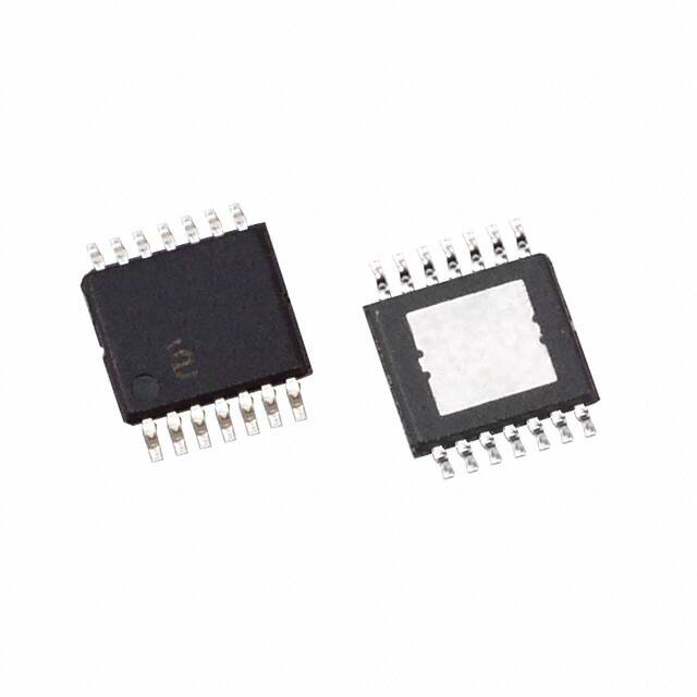


 工商网监
湘ICP备2023018690号
工商网监
湘ICP备2023018690号
