Datasheet
ISL78610
Multi-Cell Li-Ion Battery Manager
The ISL78610 Li-ion battery manager IC supervises
up to 12 series-connected cells. The part provides
accurate monitoring, cell balancing, and extensive
system diagnostics functions. Three cell balancing
modes are incorporated: Manual Balance mode,
Timed Balance mode, and Auto Balance mode. The
Auto Balance mode terminates balancing functions
when a charge transfer value specified by the host
microcontroller has been met.
The ISL78610 communicates to a host
microcontroller through an SPI interface and to other
ISL78610 devices using a robust, proprietary, 2-wire
daisy chain system.
Features
• Up to 12-cell voltage monitors with support for
Li-ion CoO2, Li-ion Mn2O4, and Li-ion FePO4
chemistries
• Board level cell voltage measurement accuracy
±1.5mV
• 13-bit cell voltage measurement
• Pack voltage measurement accuracy ±100mV
• 14-bit pack voltage and temperature measurements
• Cell voltage scan rate of 19.5µs per cell (234µs to
scan 12 cells)
The ISL78610 is offered in a 64 Ld TQFP package
and is specified for operation at a temperature range
of -40°C to +105°C.
• Internal and external temperature monitoring
Applications
• Integrated system diagnostics for all key internal
functions
• Hybrid Electric Vehicle (HEV), Plug-in Hybrid
Electric Vehicle (PHEV), and Electric Vehicle (EV)
battery packs
• Electric motorcycle battery packs
• Backup battery and energy storage systems
requiring high accuracy management and
monitoring
• Portable and semiportable equipment
• Up to four external temperature inputs
• Robust daisy chain communications system
• Hardwired and communications based fault
notification
• Integrated watchdog shuts down device if
communication is lost
• 2Mbps SPI
• AEC-Q100 qualified
Related Literature
For a full list of related documents, visit our website
• ISL78610 product page
FN8830 Rev.4.00
Jun.29.20
Page 1 of 132
�ISL78610
TO OTHER DEVICES (OPTIONAL)
ISL78610
ISL78610
VG2 VG2
VG1 VG1
DHi2
DLo2
DHi2
DHi1
DLo2
DLo1
SCLK
DOUT
DIN
CS
DATA READY
HOST
MICRO
FAULT
EN
VG1
VG1
MONITOR BOARD (MASTER OR STANDALONE)
VG2
MONITOR BOARD (DAISY CHAIN - OPTIONAL)
Figure 1. Typical Application
FN8830 Rev.4.00
Jun.29.20
Page 2 of 132
�ISL78610
Contents
1.
Overview . . . . . . . . . . . . . . . . . . . . . . . . . . . . . . . . . . . . . . . . . . . . . . . . . . . . . . . . . . . . . . . . . . . . . . . . . . 6
1.1
1.2
1.3
1.4
2.
Block Diagram . . . . . . . . . . . . . . . . . . . . . . . . . . . . . . . . . . . . . . . . . . . . . . . . . . . . . . . . . . . . . . . . . . .
Ordering Information . . . . . . . . . . . . . . . . . . . . . . . . . . . . . . . . . . . . . . . . . . . . . . . . . . . . . . . . . . . . . . .
Pin Configuration . . . . . . . . . . . . . . . . . . . . . . . . . . . . . . . . . . . . . . . . . . . . . . . . . . . . . . . . . . . . . . . . .
Pin Descriptions . . . . . . . . . . . . . . . . . . . . . . . . . . . . . . . . . . . . . . . . . . . . . . . . . . . . . . . . . . . . . . . . . .
6
7
8
8
Specifications . . . . . . . . . . . . . . . . . . . . . . . . . . . . . . . . . . . . . . . . . . . . . . . . . . . . . . . . . . . . . . . . . . . . . 10
2.1
2.2
2.3
2.4
2.5
2.6
2.7
3.
Absolute Maximum Ratings . . . . . . . . . . . . . . . . . . . . . . . . . . . . . . . . . . . . . . . . . . . . . . . . . . . . . . . . 10
Thermal Information . . . . . . . . . . . . . . . . . . . . . . . . . . . . . . . . . . . . . . . . . . . . . . . . . . . . . . . . . . . . . . .11
Recommended Operating Conditions . . . . . . . . . . . . . . . . . . . . . . . . . . . . . . . . . . . . . . . . . . . . . . . . . .11
Electrical Specifications . . . . . . . . . . . . . . . . . . . . . . . . . . . . . . . . . . . . . . . . . . . . . . . . . . . . . . . . . . . .11
Timing Diagrams . . . . . . . . . . . . . . . . . . . . . . . . . . . . . . . . . . . . . . . . . . . . . . . . . . . . . . . . . . . . . . . . . 17
Performance Characteristics . . . . . . . . . . . . . . . . . . . . . . . . . . . . . . . . . . . . . . . . . . . . . . . . . . . . . . . 18
Performance Curves . . . . . . . . . . . . . . . . . . . . . . . . . . . . . . . . . . . . . . . . . . . . . . . . . . . . . . . . . . . . . . 19
Device Description and Operation . . . . . . . . . . . . . . . . . . . . . . . . . . . . . . . . . . . . . . . . . . . . . . . . . . . . 25
3.1
3.2
3.3
4.
Cell Voltage Monitoring . . . . . . . . . . . . . . . . . . . . . . . . . . . . . . . . . . . . . . . . . . . . . . . . . . . . . . . . . . . . 25
Cell Balancing . . . . . . . . . . . . . . . . . . . . . . . . . . . . . . . . . . . . . . . . . . . . . . . . . . . . . . . . . . . . . . . . . . . 25
Power Modes . . . . . . . . . . . . . . . . . . . . . . . . . . . . . . . . . . . . . . . . . . . . . . . . . . . . . . . . . . . . . . . . . . . 25
System Hardware Connection . . . . . . . . . . . . . . . . . . . . . . . . . . . . . . . . . . . . . . . . . . . . . . . . . . . . . . . . 27
4.1
4.2
4.3
4.4
4.5
4.6
4.7
4.8
4.9
4.10
5.
Battery and Cell Balance Connection . . . . . . . . . . . . . . . . . . . . . . . . . . . . . . . . . . . . . . . . . . . . . . . . .
Power Supplies and Reference . . . . . . . . . . . . . . . . . . . . . . . . . . . . . . . . . . . . . . . . . . . . . . . . . . . . .
Communications Circuits . . . . . . . . . . . . . . . . . . . . . . . . . . . . . . . . . . . . . . . . . . . . . . . . . . . . . . . . . .
Daisy Chain Circuits . . . . . . . . . . . . . . . . . . . . . . . . . . . . . . . . . . . . . . . . . . . . . . . . . . . . . . . . . . . . . .
External Inputs . . . . . . . . . . . . . . . . . . . . . . . . . . . . . . . . . . . . . . . . . . . . . . . . . . . . . . . . . . . . . . . . . .
Typical Application Circuits . . . . . . . . . . . . . . . . . . . . . . . . . . . . . . . . . . . . . . . . . . . . . . . . . . . . . . . . .
Operating with Reduced Cell Counts . . . . . . . . . . . . . . . . . . . . . . . . . . . . . . . . . . . . . . . . . . . . . . . . .
Board Layout Notes . . . . . . . . . . . . . . . . . . . . . . . . . . . . . . . . . . . . . . . . . . . . . . . . . . . . . . . . . . . . . .
Component Selection . . . . . . . . . . . . . . . . . . . . . . . . . . . . . . . . . . . . . . . . . . . . . . . . . . . . . . . . . . . . .
Board Level Calibration . . . . . . . . . . . . . . . . . . . . . . . . . . . . . . . . . . . . . . . . . . . . . . . . . . . . . . . . . . .
27
32
33
35
36
37
38
46
47
47
System Commands . . . . . . . . . . . . . . . . . . . . . . . . . . . . . . . . . . . . . . . . . . . . . . . . . . . . . . . . . . . . . . . . . 49
5.1
5.2
5.3
5.4
5.5
5.6
5.7
5.8
5.9
5.10
5.11
5.12
5.13
5.14
5.15
5.16
Device Response . . . . . . . . . . . . . . . . . . . . . . . . . . . . . . . . . . . . . . . . . . . . . . . . . . . . . . . . . . . . . . . .
Address All . . . . . . . . . . . . . . . . . . . . . . . . . . . . . . . . . . . . . . . . . . . . . . . . . . . . . . . . . . . . . . . . . . . . .
Read and Write Commands . . . . . . . . . . . . . . . . . . . . . . . . . . . . . . . . . . . . . . . . . . . . . . . . . . . . . . . .
Scan Voltages Command . . . . . . . . . . . . . . . . . . . . . . . . . . . . . . . . . . . . . . . . . . . . . . . . . . . . . . . . . .
Scan Temperatures Command . . . . . . . . . . . . . . . . . . . . . . . . . . . . . . . . . . . . . . . . . . . . . . . . . . . . . .
Scan Mixed Command . . . . . . . . . . . . . . . . . . . . . . . . . . . . . . . . . . . . . . . . . . . . . . . . . . . . . . . . . . . .
Scan Wires Command . . . . . . . . . . . . . . . . . . . . . . . . . . . . . . . . . . . . . . . . . . . . . . . . . . . . . . . . . . . .
Scan All Command . . . . . . . . . . . . . . . . . . . . . . . . . . . . . . . . . . . . . . . . . . . . . . . . . . . . . . . . . . . . . . .
Scan Continuous Command . . . . . . . . . . . . . . . . . . . . . . . . . . . . . . . . . . . . . . . . . . . . . . . . . . . . . . . .
Scan Inhibit Command . . . . . . . . . . . . . . . . . . . . . . . . . . . . . . . . . . . . . . . . . . . . . . . . . . . . . . . . . . . .
Measure Command . . . . . . . . . . . . . . . . . . . . . . . . . . . . . . . . . . . . . . . . . . . . . . . . . . . . . . . . . . . . . .
Scan Counter . . . . . . . . . . . . . . . . . . . . . . . . . . . . . . . . . . . . . . . . . . . . . . . . . . . . . . . . . . . . . . . . . . .
Temperature Monitoring Operation . . . . . . . . . . . . . . . . . . . . . . . . . . . . . . . . . . . . . . . . . . . . . . . . . . .
Sleep Command . . . . . . . . . . . . . . . . . . . . . . . . . . . . . . . . . . . . . . . . . . . . . . . . . . . . . . . . . . . . . . . . .
Wakeup Command . . . . . . . . . . . . . . . . . . . . . . . . . . . . . . . . . . . . . . . . . . . . . . . . . . . . . . . . . . . . . . .
Reset Command . . . . . . . . . . . . . . . . . . . . . . . . . . . . . . . . . . . . . . . . . . . . . . . . . . . . . . . . . . . . . . . . .
FN8830 Rev.4.00
Jun.29.20
49
50
50
51
51
51
52
52
52
54
54
55
55
56
57
57
Page 3 of 132
�ISL78610
5.17
5.18
5.19
5.20
5.21
5.22
5.23
5.24
6.
Calc Register Checksum . . . . . . . . . . . . . . . . . . . . . . . . . . . . . . . . . . . . . . . . . . . . . . . . . . . . . . . . . .
Check Register Checksum . . . . . . . . . . . . . . . . . . . . . . . . . . . . . . . . . . . . . . . . . . . . . . . . . . . . . . . . .
Balance Enable Command . . . . . . . . . . . . . . . . . . . . . . . . . . . . . . . . . . . . . . . . . . . . . . . . . . . . . . . . .
Balance Inhibit Command . . . . . . . . . . . . . . . . . . . . . . . . . . . . . . . . . . . . . . . . . . . . . . . . . . . . . . . . . .
Cell Balancing Functions . . . . . . . . . . . . . . . . . . . . . . . . . . . . . . . . . . . . . . . . . . . . . . . . . . . . . . . . . .
Manual Balance Mode . . . . . . . . . . . . . . . . . . . . . . . . . . . . . . . . . . . . . . . . . . . . . . . . . . . . . . . . . . . .
Timed Balance Mode . . . . . . . . . . . . . . . . . . . . . . . . . . . . . . . . . . . . . . . . . . . . . . . . . . . . . . . . . . . . .
Auto Balance Mode . . . . . . . . . . . . . . . . . . . . . . . . . . . . . . . . . . . . . . . . . . . . . . . . . . . . . . . . . . . . . .
58
58
58
58
58
60
61
62
Daisy Chain Commands . . . . . . . . . . . . . . . . . . . . . . . . . . . . . . . . . . . . . . . . . . . . . . . . . . . . . . . . . . . . . 66
6.1
6.2
6.3
7.
Identify Command . . . . . . . . . . . . . . . . . . . . . . . . . . . . . . . . . . . . . . . . . . . . . . . . . . . . . . . . . . . . . . . . 66
ACK (Acknowledge) Command . . . . . . . . . . . . . . . . . . . . . . . . . . . . . . . . . . . . . . . . . . . . . . . . . . . . . 69
NAK (Not Acknowledge) Command . . . . . . . . . . . . . . . . . . . . . . . . . . . . . . . . . . . . . . . . . . . . . . . . . . 69
Communications . . . . . . . . . . . . . . . . . . . . . . . . . . . . . . . . . . . . . . . . . . . . . . . . . . . . . . . . . . . . . . . . . . . 70
7.1
7.2
7.3
7.4
7.5
7.6
7.7
7.8
7.9
8.
SPI Interface . . . . . . . . . . . . . . . . . . . . . . . . . . . . . . . . . . . . . . . . . . . . . . . . . . . . . . . . . . . . . . . . . . . .
Non-Daisy Chain Communications . . . . . . . . . . . . . . . . . . . . . . . . . . . . . . . . . . . . . . . . . . . . . . . . . . .
Daisy Chain Communications . . . . . . . . . . . . . . . . . . . . . . . . . . . . . . . . . . . . . . . . . . . . . . . . . . . . . . .
Communications Protocol . . . . . . . . . . . . . . . . . . . . . . . . . . . . . . . . . . . . . . . . . . . . . . . . . . . . . . . . . .
Daisy Chain Commands/Responses . . . . . . . . . . . . . . . . . . . . . . . . . . . . . . . . . . . . . . . . . . . . . . . . .
Communication Timing . . . . . . . . . . . . . . . . . . . . . . . . . . . . . . . . . . . . . . . . . . . . . . . . . . . . . . . . . . . .
Measurement Timing Diagrams . . . . . . . . . . . . . . . . . . . . . . . . . . . . . . . . . . . . . . . . . . . . . . . . . . . . .
Command Timing Diagram . . . . . . . . . . . . . . . . . . . . . . . . . . . . . . . . . . . . . . . . . . . . . . . . . . . . . . . . .
Response Timing Diagrams . . . . . . . . . . . . . . . . . . . . . . . . . . . . . . . . . . . . . . . . . . . . . . . . . . . . . . . .
70
71
74
74
78
81
81
84
85
System Timing Tables . . . . . . . . . . . . . . . . . . . . . . . . . . . . . . . . . . . . . . . . . . . . . . . . . . . . . . . . . . . . . . 88
8.1
8.2
8.3
9.
Command Timing Tables . . . . . . . . . . . . . . . . . . . . . . . . . . . . . . . . . . . . . . . . . . . . . . . . . . . . . . . . . . 88
Measurement Timing Tables . . . . . . . . . . . . . . . . . . . . . . . . . . . . . . . . . . . . . . . . . . . . . . . . . . . . . . . . 90
Response Timing Tables . . . . . . . . . . . . . . . . . . . . . . . . . . . . . . . . . . . . . . . . . . . . . . . . . . . . . . . . . . . 92
System Diagnostics Functions . . . . . . . . . . . . . . . . . . . . . . . . . . . . . . . . . . . . . . . . . . . . . . . . . . . . . . . 97
9.1
9.2
9.3
9.4
9.5
9.6
9.7
9.8
9.9
9.10
Hardware Fault Detection . . . . . . . . . . . . . . . . . . . . . . . . . . . . . . . . . . . . . . . . . . . . . . . . . . . . . . . . . . 97
System Out of Limit Detection . . . . . . . . . . . . . . . . . . . . . . . . . . . . . . . . . . . . . . . . . . . . . . . . . . . . . . 97
Fault Signal Filtering . . . . . . . . . . . . . . . . . . . . . . . . . . . . . . . . . . . . . . . . . . . . . . . . . . . . . . . . . . . . . . 97
Diagnostic Activity Settling Time . . . . . . . . . . . . . . . . . . . . . . . . . . . . . . . . . . . . . . . . . . . . . . . . . . . . . 99
Memory Checksum . . . . . . . . . . . . . . . . . . . . . . . . . . . . . . . . . . . . . . . . . . . . . . . . . . . . . . . . . . . . . . . 99
Communication Faults . . . . . . . . . . . . . . . . . . . . . . . . . . . . . . . . . . . . . . . . . . . . . . . . . . . . . . . . . . . . 99
Communications Failure . . . . . . . . . . . . . . . . . . . . . . . . . . . . . . . . . . . . . . . . . . . . . . . . . . . . . . . . . . 100
Daisy Chain Communications Conflicts . . . . . . . . . . . . . . . . . . . . . . . . . . . . . . . . . . . . . . . . . . . . . . 101
Loss of Signal From Host . . . . . . . . . . . . . . . . . . . . . . . . . . . . . . . . . . . . . . . . . . . . . . . . . . . . . . . . . 101
Alarm Response . . . . . . . . . . . . . . . . . . . . . . . . . . . . . . . . . . . . . . . . . . . . . . . . . . . . . . . . . . . . . . . . 103
10.
Fault Diagnostics . . . . . . . . . . . . . . . . . . . . . . . . . . . . . . . . . . . . . . . . . . . . . . . . . . . . . . . . . . . . . . . . . 104
11.
Worked Examples . . . . . . . . . . . . . . . . . . . . . . . . . . . . . . . . . . . . . . . . . . . . . . . . . . . . . . . . . . . . . . . . . 107
11.1
11.2
11.3
11.4
12.
12.1
Voltage Reference Check Calculation . . . . . . . . . . . . . . . . . . . . . . . . . . . . . . . . . . . . . . . . . . . . . . . 107
Cell Balancing – Manual Mode . . . . . . . . . . . . . . . . . . . . . . . . . . . . . . . . . . . . . . . . . . . . . . . . . . . . . 108
Cell Balancing – Timed Mode . . . . . . . . . . . . . . . . . . . . . . . . . . . . . . . . . . . . . . . . . . . . . . . . . . . . . . 108
Cell Balancing – Auto Mode . . . . . . . . . . . . . . . . . . . . . . . . . . . . . . . . . . . . . . . . . . . . . . . . . . . . . . . .110
System Registers . . . . . . . . . . . . . . . . . . . . . . . . . . . . . . . . . . . . . . . . . . . . . . . . . . . . . . . . . . . . . . . . . .115
Register Descriptions . . . . . . . . . . . . . . . . . . . . . . . . . . . . . . . . . . . . . . . . . . . . . . . . . . . . . . . . . . . . .115
FN8830 Rev.4.00
Jun.29.20
Page 4 of 132
�ISL78610
12.2
12.3
12.4
12.5
Temperature Data, Secondary Voltage Reference Data, Scan Count . . . . . . . . . . . . . . . . . . . . . . . .116
Fault Registers . . . . . . . . . . . . . . . . . . . . . . . . . . . . . . . . . . . . . . . . . . . . . . . . . . . . . . . . . . . . . . . . . .116
Reference Coefficient Registers . . . . . . . . . . . . . . . . . . . . . . . . . . . . . . . . . . . . . . . . . . . . . . . . . . . . 124
Nonvolatile Memory (EEPROM) Checksum . . . . . . . . . . . . . . . . . . . . . . . . . . . . . . . . . . . . . . . . . . . 126
13.
Register Map . . . . . . . . . . . . . . . . . . . . . . . . . . . . . . . . . . . . . . . . . . . . . . . . . . . . . . . . . . . . . . . . . . . . . 127
14.
Revision History . . . . . . . . . . . . . . . . . . . . . . . . . . . . . . . . . . . . . . . . . . . . . . . . . . . . . . . . . . . . . . . . . . 131
15.
Package Outline Drawing . . . . . . . . . . . . . . . . . . . . . . . . . . . . . . . . . . . . . . . . . . . . . . . . . . . . . . . . . . . 132
FN8830 Rev.4.00
Jun.29.20
Page 5 of 132
�ISL78610
1.1
Overview
Block Diagram
CONTROL LOGIC AND COMMUNICATIONS
1.
1. Overview
VBAT
VC12
CB12
VC11
CB11
VC10
VC8
CB8
VC7
CB7
VC6
CB6
VC5
CB5
VC4
CB4
BASE
VREG
V3P3
VDDEXT
V2P5
V2P5
VCC
VREF
MUX
CB9
REF
VC MUX
VC9
INPUT BUFFER/LEVEL SHIFT AND FAULT DETECTION
CB10
DAISY
CHAIN
AND
SPI
COMMS
DHI 2
DLO 2
SCLK/DHI 1
CS/DLO 1
DIN
DOUT
DATA READY
COMMS RATE 1
COMMS RATE 0
COMMS SELECT 2
COMMS SELECT 1
DGND
FAULT
EN
VC3
ADC
CB3
TEMPREG
VC2
CB2
CB1
VC0
IC TEMP
VC1
REFERENCE
TEMP MUX
ExT1
ExT2
ExT3
ExT4
VSS
Figure 2. Block Diagram
FN8830 Rev.4.00
Jun.29.20
Page 6 of 132
�ISL78610
1.2
1. Overview
Ordering Information
Part Number
(Notes 2, 3)
Part
Marking
Trim Voltage,
VNOM (V)
Temp. Range
(°C)
Tape and Reel
(Units) (Note 1)
Package
(RoHS Compliant)
Pkg.
Dwg. #
ISL78610ANZ
ISL78610ANZ
3.3
-40 to +105
-
64 Ld TQFP
Q64.10x10D
ISL78610ANZ-T
ISL78610ANZ
3.3
-40 to +105
1k
64 Ld TQFP
Q64.10x10D
ISL78610EVKIT1Z
Evaluation Kit
Notes:
1. See TB347 for details about reel specifications.
2. These Pb-free plastic packaged products employ special Pb-free material sets, molding compounds/die attach materials, and 100% matte
tin plate plus anneal (e3 termination finish, which is RoHS compliant and compatible with both SnPb and Pb-free soldering operations).
Pb-free products are MSL classified at Pb-free peak reflow temperatures that meet or exceed the Pb-free requirements of IPC/JEDEC J
STD-020.
3. For Moisture Sensitivity Level (MSL), see the ISL78610 product information page. For more information about handling and processing
moisture sensitive devices, see TB363.
Table 1.
Product Family
Part Number
Maximum Initial Cell Voltage Monitor Error (Note 4)
ISL78600
2.0mV
ISL78610
10.0mV
Note:
4. Conditions: Temperature = -20°C to +60°C, VCELL = 2.6V to 4.0V, limits applied to a ±3 sigma distribution.
FN8830 Rev.4.00
Jun.29.20
Page 7 of 132
�ISL78610
1.3
1. Overview
Pin Configuration
1.4
VC10
CB11
VC11
CB12
VC12
VBAT
VBAT
NC
DHi2
DLo2
NC
SCLK/DHi1
CS/DLo1
NC
DIN/NC
DOUT/NC
64
63
62
61
60
59
58
57
56
55
54
53
52
51
50
49
(64 Ld 10x10 TQFP)
Top View
VC4
12
37
DNC
CB4
13
36
V3P3
VC3
14
35
V2P5
CB3
15
34
VCC
VC2
16
33
REF
32
BASE
31
DNC
38
NC
39
11
VDDEXT
10
CB5
30
VC5
ExT4
COMMS SELECT 2
29
40
28
COMMS SELECT 1
9
ExT3
41
CB6
TEMPREG
VC6
27
COMMS RATE 1
26
42
8
NC
7
ExT2
CB7
25
COMMS RATE 0
24
DGND
43
NC
44
6
ExT1
5
VC7
23
CB8
NC
FAULT
22
DATA READY
45
21
46
4
VSS
3
VC8
VSS
CB9
20
EN
19
47
VC0
2
CB1
VC9
18
DNC
17
48
VC1
1
CB2
CB10
Pin Descriptions
Pin Name
Pin Number
Description
20, 18, 16, Battery cell voltage inputs. VCn connects to the positive terminal of CELLn and the negative terminal
VC0, VC1, VC2, VC3,
VC4, VC5, VC6, VC7, 14, 12, 10, 8, of CELLn+1. (VC12 connects only to the positive terminal of CELL12 and VC0 only connects with the
6, 4, 2, 64, negative terminal of CELL1.)
VC8, VC9, VC10,
62, 60
VC11, VC12
Cell Balancing FET control outputs. Each output controls an external FET, which provides a current
path around the cell for balancing.
CB1, CB2, CB3, CB4,
CB5, CB6, CB7, CB8,
CB9, CB10, CB11,
CB12
19, 17, 15,
13, 11, 9, 7,
5, 3, 1, 63,
61
VBAT
58, 59
Main IC supply pins. Connect to the most positive terminal in the battery string.
VSS
21, 22
Ground. These pins connect to the most negative terminal in the battery string.
ExT1, ExT2, ExT3,
ExT4
24, 26, 28,
30
External temperature monitor or general purpose inputs. The temperature inputs are intended for use
with external resistor networks using NTC type thermistor sense elements but can also be used as
general purpose analog inputs at the user’s discretion. 0V to 2.5V input range.
TEMPREG
29
Temperature monitor voltage regulator output. This switched 2.5V output supplies a reference voltage
to external NTC thermistor circuits to provide ratiometric ADC inputs for temperature measurement.
FN8830 Rev.4.00
Jun.29.20
Page 8 of 132
�ISL78610
1. Overview
Pin Name
Pin Number
Description
VDDEXT
32
External V3P3 supply input/output. Connected to the V3P3 pin through a switch, this pin can be used
to power external circuits from the V3P3 supply. The switch is open when the ISL78610 is placed in
Sleep mode.
REF
33
2.5V voltage reference decoupling pin. Connect a 2.0µF to 2.5µF X7R capacitor to VSS. Do not
connect any additional external load to this pin.
VCC
34
Analog supply voltage input. Connect to V3P3 through a 33Ω resistor. Connect a 1µF capacitor to
ground.
V2P5
35
Internal 2.5V digital supply decoupling pin. Connect a 1µF capacitor to DGND.
V3P3
36
3.3V digital supply voltage input. Connect the emitter of the external NPN regulator transistor to this
pin. Connect a 1µF capacitor to DGND.
BASE
38
Regulator control pin. Connect the external NPN transistor’s base. Do not let this pin float.
DNC
37, 39, 48
COMMS SELECT 1
41
Communications Port 1 mode select pin. Connect to V3P3 through a 1kΩ resistor for daisy chain
communications on Port 1 or to DGND for SPI operation on Port 1.
COMMS SELECT 2
40
Communications Port 2 mode select pin. Connect to V3P3 through a 1kΩ resistor to enable Port 2 or
to DGND to disable this port.
COMMS RATE 0,
COMMS RATE 1
43, 42
Daisy chain communications data rate setting. Connect to DGND (‘0’) or to V3P3 (‘1’) through a 1kΩ
resistor to select between various communication data rates.
DGND
44
Digital ground.
FAULT
45
Logic fault output. Asserted low if a fault condition exists.
DATA READY
46
SPI data ready. Asserted low when the device is ready to transmit data to the host microcontroller.
EN
47
Enable input. Tie to V3P3 to enable the part, then the device is ready after a delay of tPUD (“Power-Up
Specifications” on page 12). Tie to DGND to disable (all IC functions are turned off).
DOUT/NC
49
Serial data output (SPI) or NC (daisy chain). 0V to 3.3V push-pull output.
DIN/NC
50
Serial data input (SPI) or NC (daisy chain). 0V to 3.3V input.
CS/DLo1
52
Chip-Select, active low 3.3V input (SPI) or daisy chain Port 1 Low connection.
SCLK/DHi1
53
Serial-clock input (SPI) or daisy chain Port 1 High connection.
DHi2
56
Daisy chain Port 2 High connection.
DLo2
55
Daisy chain Port 2 Low connection.
NC
23, 25, 27,
31, 51, 54,
57
FN8830 Rev.4.00
Jun.29.20
Do not connect. Leave pins floating.
No internal connection.
Page 9 of 132
�ISL78610
2.
2.1
2. Specifications
Specifications
Absolute Maximum Ratings
Parameter (Note 5)
Minimum
Maximum
Unit
VBAT
-0.5
63
V
DHi1, DLo1, DHi2, DLo2,
-0.5
VBAT + 0.5
V
VCn (for n= 0 to 12)
-0.5
VBAT + 0.5
V
CBn (for n= 1 to 12)
-0.5
VBAT + 0.5
V
VC12
-0.5
63
V
VC11
-0.5
63
V
VC10
-0.5
63
V
VC9
-0.5
54
V
VC8
-0.5
45
V
VC7
-0.5
45
V
VC6
-0.5
36
V
VC5
-0.5
36
V
VC4
-0.5
27
V
VC3
-0.5
27
V
VC2
-0.5
18
V
VC1
-0.5
18
V
VC0
-0.5
9
V
V(VCn-1) - 0.5
V(VCn-1) + 9
V
V(VCn) - 9
V(VCn) + 0.5
V
BASE, DIN, SCLK, CS, DOUT, DATA READY, COMMS SELECT n,
TEMPREG, REF, V3P3, VCC, FAULT, COMMS RATE n, EN, VDDEXT
- 0.2
5.5
V
ExTn
- 0.2
4.1
V
V2P5
- 0.2
2.9
V
Voltage Relative to VSS, unless otherwise specified
CBn (for n= 1 to 9)
CBn (for n= 10 to 12)
ESD Rating
Value
Unit
Human Body Model (Tested per AECQ100-002)
2
kV
Capacitive Discharge Model (Tested per AECQ100-011)
2
kV
Latch-Up (Tested per AEC-Q100-004; Class 2, Level A)
100
mA
CAUTION: Do not operate at or near the maximum ratings listed for extended periods of time. Exposure to such conditions can adversely
impact product reliability and result in failures not covered by warranty.
Note:
5. DOUT, DATA READY, and FAULT are digital outputs and should not be driven from external sources. V2P5, REF, TEMPREG and BASE
are analog outputs and should not be driven from external sources.
FN8830 Rev.4.00
Jun.29.20
Page 10 of 132
�ISL78610
2.2
2. Specifications
Thermal Information
Thermal Resistance (Typical)
64 Ld TQFP Package (Notes 6, 7)
θJA (°C/W)
θJC (°C/W)
42
9
Notes:
6. JA is measured with the component mounted on a high-effective thermal conductivity test board in free air. See TB379.
7. For JC, the “case temp” location is taken at the package top center.
Parameter
Minimum
Maximum Continuous Package Power Dissipation
Storage Temperature
-55
Maximum Operating Junction Temperature
Pb-Free Reflow Profile
2.3
Maximum
Unit
400
mW
+125
°C
+125
°C
See TB493.
Recommended Operating Conditions
Parameter
Minimum
Maximum
Unit
-40
+105
°C
VBAT
6
60
V
VBAT (for Daisy Chain operation)
10
60
V
VCn - VC(n-1) (for n = 1 to 12)
-0.1
5.0
V
VC0
-0.1
+0.1
V
CBn - VC(n-1) (for n = 1 to 9)
-0.5
9.0
V
CBn - VC(n-1) (for n = 10 to 12)
-9.0
0.5
V
VC5, VC6
-0.5
36
V
DIN, SCLK, CS, COMMS SELECT 1, COMMS SELECT 2, V3P3, VCC, COMMS RATE 0,
COMMS RATE 1, EN
0
3.6
V
ExT1, ExT2, ExT3, ExT4 Input Voltage
0
2.5
V
Voltage Relative to VSS, Unless Otherwise Specified
TA, Ambient Temperature Range
2.4
Electrical Specifications
VBAT = 6 to 60V, TA = -20°C to +85°C, unless otherwise specified. Biasing setup as in Figure 45 on page 32 or equivalent.
Parameter
Symbol
Test Conditions
Min
(Note 8)
Typ
Max
(Note 8)
Unit
5
V
Measurement Specifications
Cell Voltage Input Measurement
Range
VCELL
Cell Monitor Voltage Resolution
VCELLRES
[VC(N) - VC(N-1)] LSB step size (13-bit signed
number), 5V full scale value
VCELLA
Cell Measurement Error
(Cell measurement error compared with applied
voltage with 1k series resistance in line to cell
input)
Temperature = +25°C, VCELL = 3.3V
-6.5
6.5
mV
Temperature = +85°C, VCELL = 3.3V
-25.0
25.0
mV
ISL78610 Cell Monitor Voltage
Error (Absolute)
For Performance Characteristics,
see
“Performance Characteristics” on
page 18
FN8830 Rev.4.00
Jun.29.20
VC(N) - VC(N-1). For design reference
0
0.61
mV
Page 11 of 132
�ISL78610
2. Specifications
VBAT = 6 to 60V, TA = -20°C to +85°C, unless otherwise specified. Biasing setup as in Figure 45 on page 32 or equivalent. (Continued)
Parameter
Cell Input Current
IVCELL
Note: Cell accuracy figures
assume a fixed 1kΩ resistor is
placed in series with each VCn
pin (n = 0 to 12)
VBAT Monitor Voltage Resolution
VBAT Monitor Voltage Error
Min
(Note 8)
Typ
Max
(Note 8)
Unit
VC0 input, VCELL = 0.5V to 4.95V
-2.0
-1
-0.5
µA
VC1, VC2, VC3 inputs, VCELL = 0.5V to 4.95V
-3.0
-2
-0.9
µA
VC4 input, VCELL = 0.5V to 4.95V
-0.8
0
0.9
µA
VC5, VC6, VC7, VC8, VC9, VC10, VC11 inputs,
VCELL = 0.5V to 4.95V
0.5
2
3.2
µA
VC12 input, VCELL = 0.5V to 4.95V
0.4
1
2.0
µA
Symbol
VBATRES
VBAT
Test Conditions
ADC resolution referred to input (VBAT) level. 14b
unsigned number. Full scale value = 79.67V.
-120
120
mV
Temperature = +85°C,
Measured at VBAT = 39.6V
-320
320
mV
2.475
2.525
V
VTEMP
Voltage on TEMPREG output (0 to 2mA load)
External Temperature Output
Impedance
RTEMP
Output impedance at TEMPREG pin
External Temperature Input PullUp
VEXT
REXTTEMP
mV
Temperature = +25°C,
Measured at VBAT = 39.6V
External Temperature Monitoring
Regulator
External Temperature Input
Range
4.863
ExTn input voltage range. For design reference
0.1
0
Pull-up resistor to VTEMPREG applied to each
input during measurement
VBAT = 39.6V
2.500
Ω
2344
10
-12
mV
MΩ
12
mV
External Temperature Input
Offset
VEXTOFF
External Temperature Input INL
VEXTINL
±0.3
External Temperature Input Gain
Error
VEXTG
±8
Internal Temperature Monitor
Error
VINTMON
±10
°C
Internal Temperature Monitor
Resolution
TINTRES
Output resolution (LSB/°C). 14b number
31.9
LSB/°C
Internal Temperature Monitor
Output
TINT25
Output count at +25°C
9180
Decima
l
Power-Up Condition Threshold
VPOR
VBAT voltage (rising)
Power-Up Condition Hysteresis
VPORhys
mV
18.5
mV
Power-Up Specifications
4.8
5.1
5.6
400
V
mV
Initial Power-Up Delay
tPOR
Time after VPOR condition
VREF from 0V to 0.95 x VREF(nom)
(EN tied to V3P3) Device can now communicate
27.125
ms
Enable Pin Power-Up Delay
tPUD
Delay after EN = 1 to VREF from
0V to 0.95 x VREF(nom)
(VBAT = 39.6V) - Device can now communicate
27.125
ms
FN8830 Rev.4.00
Jun.29.20
Page 12 of 132
�ISL78610
2. Specifications
VBAT = 6 to 60V, TA = -20°C to +85°C, unless otherwise specified. Biasing setup as in Figure 45 on page 32 or equivalent. (Continued)
Parameter
Symbol
Min
(Note 8)
Test Conditions
Typ
Max
(Note 8)
Unit
Supply Current Specifications
VBAT Supply Current
IVBAT
Non-daisy chain configuration. Device
enabled. No communications, ADC,
measurement, or open-wire detection
activity
IVBATMASTE Daisy chain configuration – master
device. Enabled. No communications,
R
ADC, measurement, or open-wire
detection activity
6V
35
µA
39.6V
64
µA
60V
10
Daisy chain configuration – mid stack
device. Enabled. No communications,
ADC, measurement, or open-wire
detection activity
Daisy chain configuration – top device.
Enabled. No communications, ADC,
measurement, or open-wire detection
activity
µA
39.6V
680
µA
60V
550
750
1000
µA
18
mA
6V
1020
µA
39.6V
1250
µA
60V
1000
1400
1700
µA
18
mA
6V
530
µA
39.6V
680
µA
60V
550
Peak current when daisy chain transmitting
750
1000
18
µA
mA
IVBATSLEEP1 Sleep mode
(EN = 1, daisy chain configuration)
20
35
50
µA
IVBATSLEEP2 Sleep mode
(EN = 1, stand-alone, non-daisy chain)
13
20
50
µA
Shutdown. device “off” (EN = 0)
(Daisy chain and non-daisy chain configurations)
6
15
54
µA
IVBATΔSLEEP EN = 1, daisy chain Sleep mode configuration.
VBAT current difference between any two devices
operating at the same temperature and supply
voltage
0
10.5
µA
3.5
V
IVBATSHDN
VBAT Supply Current Tracking.
Sleep Mode
µA
530
Peak current when daisy chain transmitting
IVBATTOP
96
6V
Peak current when daisy chain transmitting
IVBATMID
73
V3P3 Regulator Voltage (Normal)
V3P3N
EN = 1, Load current range 0 to 5 mA
VBAT = 39.6V
V3P3 Regulator Voltage (Sleep)
V3P3S
EN = 1, Load current range, no load, (SLEEP)
VBAT = 39.6V
V3P3 Supply Current
IV3P3
Device Enabled
No measurement activity, normal mode
VREF Reference Voltage
VREF
EN = 1, no load, normal mode
2.5
V
Switch “On” resistance, VBAT = 39.6V
12
Ω
VDDEXT Switch Resistance
VCC Supply Current
RVDDEXT
IVCC
Device enabled (EN = 1). Stand-alone or daisy
configuration. No ADC or daisy chain
communications active
3.2
2.7
0.7
2.00
IVCCACTIVE1 Device enabled (EN = 1). Stand-alone or daisy
configuration. Average current during 16ms Scan
Continuous operation. VBAT = 39.6V
FN8830 Rev.4.00
Jun.29.20
IVCCSLEEP
Device enabled (EN = 1). Sleep mode. VBAT =
39.6V
IVCCSHDN
Device disabled (EN = 0). Shutdown mode
3.35
0
1
3.25
V
1.3
5.00
mA
mA
6.0
mA
2.4
µA
1.2
9.0
µA
Page 13 of 132
�ISL78610
2. Specifications
VBAT = 6 to 60V, TA = -20°C to +85°C, unless otherwise specified. Biasing setup as in Figure 45 on page 32 or equivalent. (Continued)
Parameter
Symbol
Test Conditions
Min
(Note 8)
Typ
Max
(Note 8)
Unit
Over-Temperature Protection Specifications
Internal Temperature Limit
Threshold
TINTSD
External Temperature Limit
Threshold
TXT
Balance stops and auto scan stops.
Temperature rising or falling
150
°C
Corresponding to 0V (minimum) and VTEMPREG
(maximum)
External temperature input voltages higher than
15/16 VTEMPREG are registered as open input
faults
0
16383
Decima
l
Fault Detection System Specifications
Undervoltage Threshold
VUV
Programmable. Corresponding to 0V (minimum)
and 5V (maximum)
0
8191
Decima
l
Overvoltage Threshold
VOV
Programmable. Corresponding to 0V (minimum)
and 5V (maximum)
0
8191
Decima
l
V3P3 Power-Good Window
V3PH
3.3V power-good window high threshold.
VBAT = 39.6V
3.90
V
V3PL
3.3V power-good window low threshold.
VBAT = 39.6V
2.65
V
V2PH
2.5V power-good window high threshold.
VBAT = 39.6V
2.7
V
V2PL
2.5V power-good window low threshold.
VBAT = 39.6V
2.0
V
VVCCH
VCC power-good window high threshold.
VBAT = 39.6V
3.75
V
VVCCL
VCC power-good window low threshold.
VBAT = 39.6V
2.7
V
VRPH
VREF power-good window high threshold.
VBAT = 39.6V
2.7
V
VRPL
VREF power-good window low threshold.
VBAT = 39.6V
2.30
V
2.500
V
V2P5 Power-Good Window
VCC Power-Good Window
VREF Power-Good Window
VREF Reference Accuracy Test
VRACC
VREF value calculated using stored coefficients.
VBAT = 39.6V
(See “Voltage Reference Check Calculation” on
page 107)
Voltage Reference Check
Timeout
tVREF
Time to check voltage reference value from
power-on, enable, or wake-up
20
ms
Oscillator Check Timeout
tOSC
Time to check main oscillator frequency from
power-on, enable, or wake-up
20
ms
Oscillator Check Filter Time
tOSCF
Minimum duration of fault required for detection
100
ms
Fast Oscillator
Oscillator frequency
3.4
4
4.6
MHz
Slow Oscillator
Oscillator frequency
27.2
32
36.8
kHz
Cell Open-Wire Detection (See “Scan Wires Command” on page 52 and “Open-Wire Test” on page 99)
Open-Wire Current
IOW
ISCN bit = 0; VBAT = 39.6V
0.125
0.150
0.185
mA
ISCN bit = 1; VBAT = 39.6V
0.85
1.00
1.15
mA
Open-Wire Detection Time
tOW
Open-wire current source “on” time
Open VC0 Detection Threshold
VVC0
CELL1 negative terminal (with respect to VSS)
VBAT = 39.6V (Note 9)
1.2
1.5
1.8
V
Open VC1 Detection Threshold
VVC1
CELL1 positive terminal (with respect to VSS)
VBAT = 39.6V (Note 9)
0.6
0.7
0.8
V
FN8830 Rev.4.00
Jun.29.20
4.6
ms
Page 14 of 132
�ISL78610
2. Specifications
VBAT = 6 to 60V, TA = -20°C to +85°C, unless otherwise specified. Biasing setup as in Figure 45 on page 32 or equivalent. (Continued)
Parameter
Symbol
Test Conditions
Primary Detection Threshold,
VC2 to VC12
VVC2_12P
V(VC(n - 1)) - V(VCn), n = 2 to 12
VBAT = 39.6V (Note 9)
Secondary Detection Threshold,
VC2 to VC12
VVC2_12S
Via ADC. VC2 to VC12 only
VBAT = 39.6V (Note 9)
Min
(Note 8)
Typ
Max
(Note 8)
Unit
-2
-1.5
0
V
-100
-30
50
mV
Open VBAT Fault Detection
Threshold
VVBO
VC12 - VBAT
200
mV
Open VSS Fault Detection
Threshold
VVSSO
VSS - VC0
250
mV
Cell Balance Output Specifications
2
4
5
MΩ
CBn output on. (CB1 - CB9); VBAT = 39.6V;
device sinking current
-28
-25
-21
μA
ICBH2
CBn output on. (CB10 - CB12); VBAT = 39.6V;
device sourcing current
21
25
28
μA
Cell Balance Output Leakage in
Shutdown
ICBSD
EN = GND. VBAT = 39.6V
-500
10
700
nA
External Cell Balance FET Gate
Voltage
VGS
CBn Output on;
External 320kΩ between VCn and CBn
(n = 10 to 12) and between CBn and VCn-1
(n = 1 to 9)
7.04
8.00
8.96
V
ICB = 100µA
8.94
Cell Balance Pin Output
Impedance
RCBL
CBn output off impedance
between CB(n) to VC(n-1): Cells 1 to 9 and
between CB(n) to VC(n): Cells 10 to 12
Cell Balance Output Current
ICBH1
Internal Cell Balance Output
Clamp
VCBCL
V
Logic Inputs: SCLK, CS, DIN
Low Level Input Voltage
VIL
High Level Input Voltage
VIH
Input Hysteresis
0.8
1.75
VHYS
Input Current
IIN
Input Capacitance (Note 9)
CIN
V
250
0V < VIN < V3P3
-1
V
mV
1
µA
10
pF
0.3*V3P
3
V
Logic Inputs: EN, COMMS SELECT1, COMMS SELECT2, COMMS RATE 0, COMMS RATE 1
Low Level Input Voltage
VIL
High Level Input Voltage
VIH
Input Hysteresis
VHYS
Input Current
IIN
Input Capacitance (Note 9)
CIN
(Note
9)
0V < VIN < V3P3
0.7*V3P3
V
0.05*V3P
3
V
-1
1
µA
10
pF
Logic Outputs: DOUT, FAULT, DATA READY
Low Level Output Voltage
High Level Output Voltage
FN8830 Rev.4.00
Jun.29.20
VOL1
At 3mA sink current
0
0.4
V
VOL2
At 6mA sink current
0
0.6
V
VOH1
At 3mA source current
V3P3 –
0.4
V3P3
V
VOH2
At 6mA source current
V3P3 –
0.6
V3P3
V
Page 15 of 132
�ISL78610
2. Specifications
VBAT = 6 to 60V, TA = -20°C to +85°C, unless otherwise specified. Biasing setup as in Figure 45 on page 32 or equivalent. (Continued)
Parameter
Symbol
Test Conditions
Min
(Note 8)
Typ
Max
(Note 8)
Unit
2
MHz
200
ns
SPI Interface Timing See Figures 3 and 4
SCLK Clock Frequency
Pulse Width of Input Spikes
Suppressed
fSCLK
tIN1
Enable Lead Time
tLEAD
Clock High Time
50
Chip select low to ready to receive clock data
200
ns
tHIGH
200
ns
Clock Low Time
tLOW
200
ns
Enable Lag Time
tLAG
250
ns
Last data read clock edge to Chip Select high
Slave Access Time
tA
Chip Select low to DOUT active
200
ns
Data Valid Time
tV
Clock low to DOUT valid
350
ns
Data Output Hold Time
tHO
Data hold time after falling edge of SCLK
DOUT Disable Time
tDIS
DOUT disabled following rising edge of CS
Data Setup Time
tSU
Data input valid prior to rising edge of SCLK
100
ns
Data Input Hold Time
tHI
Data input to remain valid following rising edge of
SCLK
80
ns
0
ns
240
ns
Data Ready Start Delay Time
tDR:ST
Minimum chip select high to Data Ready low
100
ns
Data Ready Stop Delay Time
tDR:SP
Maximum chip select high to Data Ready high
750
ns
Data Ready High Time
tDR:WAIT
Minimum time between bytes
1.0
µs
Chip Select High Time
tCS:WAIT
Minimum high time for CS between bytes
200
ns
Maximum time the CS remains high before SPI
communications time out - requiring the start of a
new command
100
µs
SPI Communications Timeout
tSPI:TO
DOUT Rise Time
tR
Up to 50pF load
30
ns
DOUT Fall Time
tF
Up to 50pF load
30
ns
Daisy Chain Communications Interface: DHi1, DLo1, DHi2, DLo2
Daisy Chain Clock Frequency
Comms Rate (0, 1) = 11
450
500
550
kHz
Comms Rate (0, 1) = 10
225
250
275
kHz
Comms Rate (0, 1) = 01
112.5
125
137.5
kHz
Comms Rate (0, 1) = 00
56.25
62.5
68.75
kHz
Common-Mode Reference
Voltage
VBAT/
2
V
Notes:
8. Compliance to datasheet limits is assured by one or more methods: production test, characterization, and/or design. Limits are 100%
tested, unless declared otherwise.
9. These MIN and/or MAX values are based on characterization data and are not 100% tested.
10. Stresses may be induced in the ISL78610 during soldering or other high temperature events that affect measurement accuracy. Initial
accuracy does not include effects due to this. See Figure 8 on page 19 for cell reading accuracy obtained after soldering to Renesas
evaluation boards. When soldering the ISL78610 to a customized circuit board with a layout or construction significantly differing from the
Renesas evaluation board, design verification tests should be applied to determine drift due to soldering and over lifetime.
FN8830 Rev.4.00
Jun.29.20
Page 16 of 132
�ISL78610
2.5
2. Specifications
Timing Diagrams
CS
(FROM µC)
tSPI:TO
tLEAD
tHIGH
tLOW
tCS:WAIT
tLAG
SCLK
(FROM µC)
tA
tF
tV
tDIS
tHO
DOUT
(TO µC)
tSU
tR
tHI
DIN
(FROM µC)
CLOCK DATA INTO
ISL78610
CLOCK DATA OUT OF
ISL78610
Figure 3. SPI Full Duplex (4-Wire) Interface Timing
tCS:WAIT
tSPI:TO
CS
(FROM µC)
tDR:WAIT
tDR:SP
DATA READY
(TO µC)
SCLK
(FROM µC)
tA
tDIS
DOUT
(TO µC)
CLOCK DATA OUT OF
ISL78610
DIN
(FROM µC)
SIGNALS ON DIN IGNORED
WHILE DATA READY IS LOW
CLOCK DATA INTO
ISL78610
Figure 4. SPI Half Duplex (3-Wire) Interface Timing
FN8830 Rev.4.00
Jun.29.20
Page 17 of 132
�ISL78610
2.6
2. Specifications
Performance Characteristics
Table 2.
Cell/VBAT Reading Error - 3 Sigma
Parameter
ISL78610 Initial Cell
Reading Error (Absolute)
ISL78610 Initial VBAT
Reading Error (Absolute)
Symbol
VCELLA
VBAT
Test Conditions
-3 Sigma
(Note 11)
+3 Sigma
(Note 11)
Unit
Temperature = +25°C
VCELL = 3.3V
Limits applied to a ±3 sigma distribution
-3.2
3.2
mV
Temperature = -20°C to +60°C
VCELL = 2.6V to 4.0V
Limits applied to a ±3 sigma distribution
-10
10
mV
Temperature = -40°C to -20°C
VCELL = 2.6V to 4.0V
Limits applied to a ±3 sigma distribution
-15
15
mV
Temperature = +60°C to +85°C
VCELL = 2.6V to 4.0V
Limits applied to a ±3 sigma distribution
-15
15
mV
Temperature = -20°C to +60°C
VBAT = 31.2V to 48V
Limits applied to a ±3 sigma distribution
-175
175
mV
Temperature = -40°C to +105°C
VBAT = 31.2V to 48V
Limits applied to a ±3 sigma distribution
-300
300
mV
Voltage Reference Long
Term Drift
Table 3.
Typ
-0.31
mV/
log (days)
Cell/VBAT Reading Error - 5 Sigma
Parameter
Symbol
ISL78610 Initial Cell Monitor
Voltage Error (Absolute)
VCELLA
ISL78610 Initial VBAT
Reading Error (Absolute)
VBAT
Test Conditions
-5 Sigma
(Note 11)
Typ
+5 Sigma
(Note 11)
Unit
Temperature = +25°C
VCELL = 3.3V
Limits applied to a ±5 sigma distribution
-5
5
mV
Temperature = -20°C to +60°C
VCELL = 2.6V to 4.0V
Limits applied to a ±5 sigma distribution
-12
12
mV
Temperature = -40°C to -20°C
VCELL = 2.6V to 4.0V
Limits applied to a ±5 sigma distribution
-20
20
mV
Temperature = +60°C to +85°C
VCELL = 2.6V to 4.0V
Limits applied to a ±5 sigma distribution
-25
25
mV
Temperature = +85°C to +105°C
VCELL = 2.6V to 4.0V
Limits applied to a ±5 sigma distribution
-45
45
mV
Temperature = -20°C to +60°C
VBAT = 31.2V to 48V
Limits applied to a ±5 sigma distribution
-250
250
mV
Temperature = -40°C to +105°C
VBAT = 31.2V to 48V
Limits applied to a ±5 sigma distribution
-425
425
mV
Note:
11. These distribution values are based on characterization of devices mounted on evaluation boards and are not 100% tested.
FN8830 Rev.4.00
Jun.29.20
Page 18 of 132
�ISL78610
2.7
2. Specifications
Performance Curves
20
50
15
40
READING ERROR (mV)
READING ERROR (mV)
These performance curves are based on characterization of devices mounted on evaluation boards.
10
5
0
-5
-10
-15
30
20
10
0
-10
-20
-30
-40
-50
-20
0.5
2.6
3
3.3
3.6
4
4.5
-40
-20
0
20
Figure 5. Cell Voltage Reading Error From -20°C to +60°C
80
100
120
35
PERCENTAGE OF CELLS (%)
PERCENTAGE OF CELLS (%)
60
Figure 6. Cell Voltage Reading Error 3.0V to 3.6V Per Cell
40.0
35.0
30.0
25.0
20.0
15.0
10.0
5.0
0.0
30
25
20
15
10
5
0
-1.5
-1
-0.5
0
0.5
1
1.5
2
2.5
3
3.5
-4
-3
-2
-1
READING ERROR (mV)
200
150
102
105
108
103
106
109
READING ERROR (mV)
250
100
50
0
-50
-100
-150
0
5
10
15
20
25
30
35
40
45
50
55
PACK VOLTAGE (V)
Figure 9. Pack Voltage Reading Error at +25°C
(Multiple Boards)
FN8830 Rev.4.00
Jun.29.20
1
2
3
4
5
6
7
8
9
10
Figure 8. Cell Reading Error from Evaluation Boards at
Cell Voltage from 2.6V to 4.0V,
and -20°C to +60°C Histogram
300
101
104
107
110
0
READING ERROR (mV)
Figure 7. Initial Cell Voltage Accuracy from Evaluation
Boards at 3.3V, +25°C Histogram
READING ERROR (mV)
40
o
TEMPERATURE ( C)
CELL VOLTAGE (V)
60
180
160
140
120
100
80
60
40
20
0
-20
-40
-60
6V
36V
43.2V
54V
-40
10
60
31.2V
39.6V
48V
110
160
TEMPERATURE (oC)
Figure 10. Average Pack Voltage Reading Error at 6V to
54V Pack Voltage
Page 19 of 132
�ISL78610
2. Specifications
These performance curves are based on characterization of devices mounted on evaluation boards. (Continued)
30.0
5.00
4.00
READING ERROR (°C)
PERCENTAGE (%)
25.0
20.0
15.0
10.0
5.0
3.00
2.00
1.00
0.00
-1.00
-2.00
6V
36V
43.2V
54V
-3.00
-4.00
0.0
-5.00
-140
-100
-60
-20
20
60
100
140
180
-40 -30 -20 -10 0
10 20 30 40 50 60 70 80 90 100 110
o
TEMPERATURE ( C)
READING ERROR (mV)
Figure 11. Initial Pack Voltage Accuracy 31.2V to 48V,
-20°C to +60°C Histogram
Figure 12. IC Temperature Reading Error vs Temperature
6V
36V
43.2V
54V
4.00
3.00
2.00
CELL MEASUREMENT ERROR (mV)
2ND REFERENCE ERROR (mV)
5.00
31.2V
39.6V
48V
1.00
0.00
-1.00
-2.00
-3.00
-4.00
-5.00
-40 -30 -20 -10 0
10 20 30 40 50 60 70 80 90 100 110
0
-0.2
-0.4
-0.6
-0.8
-1.0
-1.2
-1.4
0.001
0.01
0.1
YEARS
TEMPERATURE (oC)
Figure 13. Voltage Reference Check Voltage Error Over
VBAT = 6V to 54V and Temperature
1.0
10.0
Figure 14. Long Term Drift
25.60
25.6
BALANCE CURRENT (µA)
BALANCE CURRENT (µA)
31.2V
39.6V
48V
25.55
25.50
25.45
25.4
VCELL = 3.3V
25.2
25.0
24.8
24.6
24.4
25.40
0
10
20
30
40
PACK VOLTAGE (V)
50
Figure 15. Balance Current vs Pack Voltage
FN8830 Rev.4.00
Jun.29.20
60
24.2
-40
-20
0
20
40
60
TEMPERATURE (°C)
80
100
Figure 16. Balance Current vs Temperature
Page 20 of 132
�ISL78610
2. Specifications
These performance curves are based on characterization of devices mounted on evaluation boards. (Continued)
1000
975
980
VCELL = 3.3V
TEMPERATURE = +25°C
960
970
965
IOPWI (µA)
IOPWI (µA)
940
960
920
900
880
860
840
955
820
800
950
-40
-20
0
20
40
60
80
100
120
0
10
20
TEMPERATURE ( oC )
Figure 17. Open-Wire Test Current vs Temperature
(1mA Setting)
50
60
158.6
159
158.4
VCELL = 3.3V
158
TEMPERATURE = +25°C
158.2
157
IOPWI (µA)
IOPWI (µA)
40
Figure 18. Open-Wire Test Current vs Pack Voltage
(1mA Setting)
160
156
155
158
157.8
157.6
154
157.4
153
157.2
152
157
-40
-20
0
20
40
60
80
100
0
120
10
20
o
Figure 19. Open-Wire Test Current vs Temperature
(150µA Setting)
4.05
30
40
50
60
PACK VOLTAGE (V)
TEMPERATURE ( C )
Figure 20. Open-Wire Test Current vs Pack Voltage
(150µA Setting)
4.045
VBAT = 39.6V
4.040
FREQUENCY (MHz)
4.00
FREQUENCY (MHz)
30
PACK VOLTAGE (V)
3.95
3.90
3.85
3.80
VBAT = 39.6V
4.035
4.030
4.025
4.020
4.015
4.010
3.75
4.005
3.70
4.000
-40
-20
0
20
40
60
80
100
120
TEMPERATURE ( oC )
Figure 21. 4MHz Oscillator Frequency vs Temperature
FN8830 Rev.4.00
Jun.29.20
2.5
2.7
2.9
3.1
3.3
3.5
3.7
3.9
VCC (V)
Figure 22. 4MHz Oscillator Frequency vs VCC
Page 21 of 132
�ISL78610
2. Specifications
These performance curves are based on characterization of devices mounted on evaluation boards. (Continued)
31.60
31.35
31.40
FREQUENCY (kHz)
FREQUENCY (kHz)
31.30
VBAT = 39.6V
31.20
31.00
30.80
30.60
30.40
30.20
VBAT = 39.6V
31.25
31.20
31.15
31.10
31.05
30.00
31.00
29.80
-40
-20
0
20
40
60
80
100
2.5
120
2.7
2.9
3.1
TEMPERATURE ( oC )
Figure 23. 32kHz Oscillator Frequency vs Temperature
3.7
3.9
80
50
70
VBAT = 60V
IVBAT (µA)
30
VBAT = 39.6V
20
VBAT = 60V
60
40
IVBAT (µA)
3.5
Figure 24. 32kHz Oscillator Frequency vs VCC
60
VBAT = 6V
50
VBAT = 39.6V
40
30
20
10
VBAT = 6V
10
0
0
-40
-20
0
20
40
60
80
100
-40
120
-20
0
80
70
70
80
100
120
60
VBAT = 60V
IVBAT (µA)
50
VBAT = 39.6V
30
VBAT = 6V
20
60
Figure 26. Pack Voltage Sleep Current vs Temperature at
6V, 39.6V, 60V (Daisy Chain Master)
80
40
40
TEMPERATURE ( C )
Figure 25. Pack Voltage Sleep Current vs Temperature at
6V, 39.6V, 60V (Stand-Alone Mode)
60
20
o
o
TEMPERATURE ( C )
IVBAT (µA)
3.3
VCC (V)
50
VBAT = 39.6V
VBAT = 60V
40
VBAT = 6V
30
20
10
10
0
0
-40
-20
0
20
40
60
80
100
120
o
TEMPERATURE ( C )
Figure 27. Pack Voltage Sleep Current vs Temperature at
6V, 39.6V, 60V (Daisy Chain Middle)
FN8830 Rev.4.00
Jun.29.20
-40
-20
0
20
40
60
80
100
120
o
TEMPERATURE ( C )
Figure 28. Pack Voltage Sleep Current vs Temperature at
6V, 39.6V, 60V (Daisy Chain Top)
Page 22 of 132
�ISL78610
2. Specifications
These performance curves are based on characterization of devices mounted on evaluation boards. (Continued)
750
100
VBAT = 60V
95
700
90
650
80
IVBAT (µA)
IVBAT (µA)
85
VBAT = 60V
75
70
65
VBAT = 39.6V
600
550
VBAT = 6V
60
VBAT = 39.6V
55
50
-40
-20
0
20
VBAT = 6V
500
40
60
80
100
450
120
-40
-20
0
TEMPERATURE (oC )
Figure 29. Pack Voltage Supply Current vs Temperature at
6V, 39.6V, 60V (Stand-Alone Mode)
750
VBAT = 60V
60
80
100
120
VBAT = 60V
700
1250
650
1150
IVBAT (µA)
IVBAT (µA)
40
Figure 30. Pack Voltage Supply Current vs Temperature at
6V, 39.6V, 60V (Daisy Chain Master)
1450
1350
20
TEMPERATURE (oC )
VBAT = 39.6V
1050
VBAT = 6V
950
VBAT = 39.6V
600
550
VBAT = 6V
500
450
850
-40
-20
0
20
40
60
80
100
-40
120
-20
0
20
40
60
80
100
120
o
TEMPERATURE (oC )
TEMPERATURE ( C )
Figure 31. Pack Voltage Supply Current vs Temperature at
6V, 39.6V, 60V (Daisy Chain Middle)
Figure 32. Pack Voltage Supply Current vs Temperature at
6V, 39.6V, 60V (Daisy Chain Top)
3.45
60
3.40
3.35
3.25
40
30
VBAT = 60V
IVCC (mA)
IVBAT (µA)
50
VBAT = 39.6V
20
3.20
3.15
3.10
3.05
3.00
10
2.95
VBAT = 6V
0
-40
-20
0
20
40
60
80
100
120
TEMPERATURE (oC )
Figure 33. Pack Voltage Shutdown Current vs Temperature
(EN = 0) at 6V, 39.6V, 60V
FN8830 Rev.4.00
Jun.29.20
2.90
-60
-40
-20
0
20
40
60
80
100
120
TEMPERATURE (°C)
Figure 34. VCC Supply Current vs Temperature at
6V, 39.6V, 60V
Page 23 of 132
�ISL78610
2. Specifications
These performance curves are based on characterization of devices mounted on evaluation boards. (Continued)
2.5
1.06
2.0
CELL INPUT CURRENT (µA)
SUPPLY CURRENT (mA)
1.05
1.04
39.6V
1.03
60V
1.02
6V
1.01
1.00
0.99
-40
-20
0
20
40
60
80
100
VCELL = 3.3V
1.5
VC11
VC5
VC10
1.0
0
-1.0
VC6
VC0
-1.5
-2.5
-40
VC9
VC4
-0.5
-2.0
VC7
VC12
0.5
VC3
VC2
-20
0
TEMPERATURE (°C)
Figure 35. V3P3 Supply Current vs Temperature
VC8
VC1
20
40
60
TEMPERATURE (°C)
80
100
120
Figure 36. Cell Input Current vs Temperature
CELL INPUT CURRENT (µA)
2.5
2.0 VC11
VC10
VC9
1.5 VC8
VC7
1.0 VC6
VC5
0.5
VC12
VC4
0.0
-0.5
VC0
-1.0
-1.5
VC3
-2.0 VC2
VC1
-2.5
0
10
20
30
40
PACK VOLTAGE (V)
50
60
Figure 37. Cell Input Current vs Pack Voltage (+25°C)
FN8830 Rev.4.00
Jun.29.20
Page 24 of 132
�ISL78610
3.
3. Device Description and Operation
Device Description and Operation
The ISL78610 is a Li-ion battery manager IC that supervises up to 12 series-connected cells. Up to 14 ISL78610
devices can be connected in series to support systems with up to 168 cells. The ISL78610 provides accurate
monitoring, cell balance control, and diagnostic functions. The ISL78610 includes a voltage reference, 14-bit A/D
converter, and registers for control and data.
When multiple ISL78610 devices are connected to a series of cells, their power supply domains are normally nonoverlapping. The lower (VSS) supply of each ISL78610 nominally connects to the same potential as the upper
(VBAT) supply of the ISL78610 device below.
3.1
Cell Voltage Monitoring
Within each device, the cell voltage monitoring system has two basic elements: a level shift to eliminate the cell
common-mode voltage, and an analog-to-digital conversion of the cell voltage.
Each ISL78610 is calibrated at a specific cell input voltage value, VNOM. Cell voltage measurement error data is
given in “Measurement Specifications” on page 11 for various voltage and temperature ranges with voltage
ranges defined with respect to VNOM. Plots showing the typical error distribution over the full input range are
included in “Performance Curves” on page 19.
To collect cell voltage and temperature measurements, the ISL78610 provides two multiple parameter
measurement “scanning” modes in addition to single parameter direct measurement capability. The scanning
modes provide pseudo-simultaneous measurement of all cell voltages in the stack.
The ISL78610 does not measure current. The system performs this separately using other measurement
systems.
The only filtering applied to the ADC measurements is that resulting from external protection circuits and the
limited bandwidth of the measurement path. No additional filtering is performed within the part. This arrangement
is typically needed to maintain timing integrity between the cell voltage and pack current measurements.
However, the ISL78610 does apply filtering to the fault detection systems.
3.2
Cell Balancing
Cell balancing is an important function in a battery pack consisting of a stack of multiple Li-ion cells. As the cells
charge and discharge, differences in each cell’s ability to take on and give up charge, typically leads to cells with
different states of charge. The problem with a stack of cells having different states of charge is that Li-ion cells
have a maximum voltage, above which it should not be charged, and a minimum voltage, below which it should
not be discharged. The extreme case, where one cell in the stack is at the maximum voltage and one cell is at the
minimum voltage, results in a nonfunctional battery stack, because the battery stack cannot be charged or
discharged.
The ISL78610 provides multiple cell balance modes: Manual Balance mode, Timed Balance mode, and Auto
Balance mode. These are described in more detail in “Alarm Response” on page 103.
The ISL78610 incorporates extensive fault diagnostics functions, which include cell overvoltage and
undervoltage, regulator and oscillator operation, open cell input detection, and communication faults. The current
status of most faults is accessible using the ISL78610 registers. Some communication faults are reported by
special responses to system commands and some as “unprompted” responses from the device detecting the fault
to the host microcontroller through the daisy chain.
3.3
Power Modes
To conserve power, the ISL78610 has three main power modes: Normal mode, Sleep mode, and “off” (Shutdown
mode).
FN8830 Rev.4.00
Jun.29.20
Page 25 of 132
�ISL78610
3.3.1
3. Device Description and Operation
Sleep Mode
The device enters Sleep mode in response to a Sleep command or after a watchdog timeout (see “Watchdog
Function” on page 102.) Only the communications input circuits, low speed oscillator and internal registers are
active in Sleep mode, allowing the part to perform timed scan and balancing activity and to wake up in response
to communications.
3.3.2
Shutdown Mode (Hardware Reset)
The device is in Shutdown mode when the Enable pin is low. In this mode, the internal bias for most of the IC is
powered down except digital core, sleep mode regulators, and digital input buffers. When exiting, the device
powers up and does not reload the factory programmed configuration data from the EEPROM.
The host can perform a hardware reset by toggling the EN pin low, then high. This resets the hardware but does
not reload the registers. After waiting for a tUV settling time, see “Power-Up Specifications” on page 12 the host
must perform a new IDENTIFY sequence (see “Identify Command” on page 66). Also, since the hardware reset
does not recall the EEPROM values, it is recommended that a Reset command “Reset Command” on page 57 be
sent to each device to ensure that EEPROM values have been properly recalled. The following is the
recommended sequence following a hardware reset.
1. Switch EN on.
2. Wait the required delay (tUV “Power-Up Specifications” on page 12) after re-enabling the parts.
3. Identify devices
4. Send Reset command to each device starting from the top device.
(This operation recalls the EEPROM values and performs an EEPROM checksum calculation.)
5. Identify devices again (Identify is required after a software reset)
6. The host checks the EEPROM MISR Data Register and MISR Calculated Checksum register on all devices.
These two register values should match (see “Memory Checksum” on page 99).
7. Re-load all non-default setup parameters (like OV/UV limits) to all devices.
8. The host sends a Calc Register Checksum command to each device (see “Calc Register Checksum” on
page 58).
9. The host sends a Check Register checksum to verify that there is no error (see “Check Register Checksum”
on page 58). If there is a mismatch, the device sends a fault response back to the host (see “Memory
Checksum” on page 99).
3.3.3
Normal Mode
Normal mode consists of an active state and a standby state. In the standby state, all systems are powered and
the device is ready to perform an operation in response to commands from the host microcontroller. In the Active
state, the device is performing an operation, such as ADC conversion, open-wire detection, etc.
FN8830 Rev.4.00
Jun.29.20
Page 26 of 132
�ISL78610
4.
4.1
4. System Hardware Connection
System Hardware Connection
Battery and Cell Balance Connection
The first consideration in designing a battery system around the ISL78610 is the connection of the cells to the IC.
The battery connection elements are split between the cell monitor connections (VCn) and the cell balance
connections (CBn).
4.1.1
Battery Connection
All inputs to the ISL78610 VCn pins are protected against battery voltage transients by external RC filters. The
basic input filter structure, with capacitors to the local ground, provides protection against transients and EMI for
the cell inputs. They carry the loop currents produced by EMI and should be placed as close to the battery
connector as possible. The ground terminals of the capacitors must be connected directly to a solid ground plane.
Do not use vias to connect these capacitors to the input signal path or to ground. Any vias should be placed in line
to the signal inputs so that the inductance of these forms a low pass filter with the grounded capacitors.
The resistors on the input filter provide a current limit function during hot plug events. The ISL78610 is calibrated
for use with 1kΩ series protection resistors at the VCn inputs. The VBAT connection uses a lower value input
resistor to accommodate the supply current of the ISL78610. As much as possible, the time constant produced by
the filtering applied to VBAT should be matched to that applied to the VCn monitoring inputs (see Figure 38).
LOCATE CLOSE
TO INPUT CONNECTOR
B14b
*EXAMPLE DIODE:
PTVS58VS1UTR
27
C1
820
B12
ISL78610
VBAT
58V*
VSS
180
VC12
22nF
820
B11
180
VC11
22nF
820
B10
180
VC10
22nF
820
B9
180
VC9
22nF
820
B3
180
22nF
820
B2
180
VC3
VC2
22nF
820
B1
180
VC1
22nF
820
B0
22nF
B0b
180
VC0
VSS
= “QUIET” GROUND
= “NOISY” GROUND
CELL BALANCE CIRCUITS NOT SHOWN IN THIS FIGURE
Figure 38. Typical Input Filter
FN8830 Rev.4.00
Jun.29.20
Page 27 of 132
�ISL78610
4. System Hardware Connection
The filtered battery voltage connects to the internal cell voltage monitoring system. The monitoring system is
made up of three basic elements: a level shifter to eliminate the cell common-mode voltage, a multiplexer to
select a specific input, and an analog-to-digital conversion of the cell voltage.
Each ISL78610 is calibrated at a specific cell input voltage value, VNOM with an expected input series resistance
of 1kΩ. Cell voltage measurement error data is given in “Measurement Specifications” on page 11 for various
voltage and temperature ranges with voltage ranges defined with respect to VNOM. Plots showing the typical error
distribution over the full input range are included in “Performance Curves” on page 19.
Another important consideration is the connection of cells in a stacked (non-overlapping) configuration. Mainly,
this involves how to connect the supply and ground pins at the junction of two devices. The diagram in Figure 39
shows the recommended minimum connection to the pack. It is preferred that there be four connection wires at
the intersection of two devices, but this does pose a cost constraint. To minimize the connections, the power and
monitor pins are connected separately, as shown in Figure 39. It is not recommended that all four wires connect
together with a single wire to the pack. There are two reasons for this. First, the power supply current for the
devices might affect the accuracy of the cell voltage readings. Second, if the single wire breaks, it is very difficult
for the system to tell specifically what happened through normal diagnostic methods.
An alternative circuit in Figure 40 shows the connection of one (or two) wires with additional Schottky diodes to
provide supply current paths to allow the device to detect a connection fault and to minimize the effects on cell
voltage measurements when there is an open connection to the battery.
100
820
ISL78610
VC2
VSS2
100
VC1
22nF
VSS2
820
100
VC0
22nF
VSS2
ISL78610
VBAT
27
VSS
820
BOARD
CONNECTIONS
VC0
22nF
VSS2
ISL78610
VBAT
27
C1
VSS
22nF
22nF
VSS2 180
820
820
VC12
VC11
VSS
VSS
180
VC12
22nF
820
100
VC1
22nF
VSS
100
VSS
VSS2 180
820
C1
820
VC2
22nF
22nF
820
ISL78610
180
820
VSS
180
VC11
22nF
BOARD
CONNECTIONS
VSS
Figure 39. Battery Connection Between Stacked Devices Figure 40. Battery Connection Between Stacked Devices
(Option 1)
(Option 2)
4.1.2
Cell Balance Connection
The ISL78610 uses external MOSFETs for cell balancing. The gate drive for these is derived from on-chip current
sources on the ISL78610, which are 25µA nominally. The current sources are turned on and off as needed to
control the external MOSFET devices. The current sources are turned off when the device is in Shutdown mode
or Sleep mode. The ISL78610 uses a mix of N-channel and P-channel MOSFETs for the external balancing
function. The top three cell locations, Cells 10, 11, and 12 are configured to use P-channel MOSFETs while the
remaining cell locations, Cells 1 through 9 use N-channel MOSFETs. The mix of N-channel and P-channel devices
are used for the external FETs in order to remove the need for a charge pump, while providing a balance FET gate
voltage that is sufficient to drive the FET on, regardless of the cell voltages.
FN8830 Rev.4.00
Jun.29.20
Page 28 of 132
�ISL78610
4. System Hardware Connection
Figures 41 and 42 show the circuit detail for the recommended balancing and cell voltage monitoring system. In
this configuration, the cell voltage is monitored after the cell balance resistor. This allows the system to monitor
the operation of the external balance circuits and is part of the fault detection system. However, this connection
prevents monitoring the cell voltage while cell balance is enabled for that cell.
Figure 41 shows the connection for VC12 to VC9. This connection for the upper 3 cells uses P-channel FETs,
while VC9 and below use N-channel FETs. Similarly, Figure 42 shows the connection for VC1 to VC3, using an Nchannel FETs, with the connections for VC3 through VC9 being similar. See Figure 52 on page 40 for a more
complete example.
R2
R5
VC12
22nF
C1
R1
Q1
C3
9V
100Ω
R3
R5
C1
R1
Q1
R3
R1
Q1
R5
R1
R4
R6
100Ω
R4
R6
100Ω
25µA
Q2
Q2
9V
100Ω
CB2
10kΩ
C1
25µA
R1
4MΩ
R3
VC9
22nF
C3
Q2
CB9
VC1
25µA
CB1
10kΩ
C1
R1
4MΩ
R2
4MΩ
22nF
R5
C3
25µA
9V
R5
9V
22nF
C2
R1
R3
25µA
C3
4MΩ
10kΩ
C1
VC2
22nF
C2
100Ω
22nF
R5
CB10
100Ω
C2
4MΩ
R3
VC10
C3
10kΩ
C2
10kΩ
C1
9V
22nF
C1
CB3
CB11
10kΩ
C2
Q2
4MΩ
C3
25µA
C3
VC11
22nF
VC3
22nF
C2
25µA
100Ω
100Ω
R5
R3
CB12
10kΩ
C2
4MΩ
9V
R5
VC0
22nF
VSS
VC8
ISL78610
ISL78610
Figure 41. Cell Monitor and Balance Circuit Arrangement Figure 42. Cell Monitor and Balance Circuit Arrangement
(VC8 to VC12)
(VC0 to VC3)
Table 4.
ISL78610 Input Filter Component Options
Q1 (P-channel)
with examples
Q2 (N-channel)
with examples
C1
C2
C3
R1
R2
R3
R4
R5
R6
30V A&O Semi AO3401
30V
A&O Semi AO3402
10nF
1nF
Not
populated
100k
820
720
1.54k
180
360
30V A&O Semi AO3401
30V
A&O Semi AO3402
10nF
1nF
100nF
100k
100
0
0
910
1900
60V Fairchild FDN5618
60V
Diodes DMN6140L-7
10nF
Not needed
Not
populated
330k
820
720
1.54k
180
360
60V Fairchild FDN5618
60V
Diodes DMN6140L-7
10nF
Not needed
100nF
330k
100
0
0
910
1900
Note: Q1 and Q2 should have low rDS(ON) specifications ( 1*tDAISY)
Figure 74. Command Timing to Avoid Daisy Buffer Underflow
7.4.2
Daisy Chain Receive Buffer
A 4-byte data buffer is provided between the Daisy Chain and SPI communications. This accommodates all single
transaction responses. Multiple byte responses, such as Identify, Read All Voltages, Read All Temperatures,
Read All Faults, and responses that may include a fault response from a device detecting an error, would overflow
this buffer. It is important therefore that the host microcontroller completes a read of the first byte of data before a
fifth byte arrives on the Master device’s daisy chain port and to clock data out from the SPI port faster than data is
clocked in through the Daisy port so as not to risk losing data.
For example, when performing the first step in an IDENTIFY operation (see Identify Command) the daisy chain
top device returns a 4-byte response plus 14 extra zeros (because it does not yet know how many devices are in
the stack.) If the Host does not read the first byte from the Master before the 32nd daisy clock, the extra zeros
overwrite the first byte of the response. In another example, a Read All Faults returns 22 bytes. It is important for
the Host to read data from the ISL78610 faster than 4 bytes every 31.5 Daisy clocks. (see Figure 75).
DOUT
CS
RECEIVE IDENTIFY RESPONSE
SCK
≤ 31.5 tD
≤ 31.5 tD
DATA READY
Daisy Clocks
Master
Daisy Port
DHI2/DLO2
8* tD
8* tD
8* tD
8* tD
8* tD
8* tD
8* tD
8* tD
8* tD
8* tD
8* tD
8* tD
Extra Bytes during “Read All” responses, fault responses, and first Identify Response.
A fault response may precede command response, increasing number of returned bytes.
The first Identify Response has 14 extra clocks, because stack size is not yet known.
SPI must clock out 4 bytes before the Daisy can clock in 4 bytes to prevent buffer overflow
Figure 75. Example Worst Case Timing to Avoid Daisy Buffer Overflow
FN8830 Rev.4.00
Jun.29.20
Page 76 of 132
�ISL78610
7.4.3
7. Communications
Communication Sequences
All daisy chain device responses are 4-byte sequences, except for the responses to the Read All command. All
responses start with the Device Address and use a 4-bit CRC. The response to the “Read All Commands” is to
send a normal 4-byte data response for the first data segment and continue sending the remaining data segments
in 3-byte sections composed of data address, data, and CRC. This creates an anomaly with the normal CRC
usage in that the first four bytes have a 4-bit CRC at the end (operating on 3.5 bytes of data) while the remaining
bytes have a CRC, which only operates on 2.5 bytes. The host microcontroller, having requested the data, must
be prepared for this.
Daisy chain devices require Device Address information to be added to the basic command set. Daisy chain
writes are 4-byte sequences. Daisy chain reads are three bytes. All commands, except register write operations,
are treated as reads. Daisy chain communications employ a 4-bit CRC (Cyclic Redundancy Check) using a
polynomial of the form 1 + X + X4. The first four bits of each daisy chain transmission contain the Device Address,
which can be any number from 0001 to 1110. All devices respond to the “Address All” (1111) and Identify (0000)
Device Addresses. The fifth bit is set to ‘1’ for write and ‘0’ for read. The rules for daisy chain installations are
shown in Table 31.
Table 31. ISL78610 Data Interpretation Rules for Daisy Chain Installations
Fifth Bit
(R/W)
Page
Data
Address
Interpretation
Device Address [3:0] (Nonzero)
0
011
001000
Measure command. Data address is followed by 6-bit element address.
0000
0
011
001001
Identify command. Data address is followed by device count data.
Device Address [3:0] (Nonzero)
0
Any
All other
Device Read command. Data address is followed by 6 zeros.
Device Address [3:0] (Nonzero)
1
Any
Any
First Four Bits in Sequence
7.4.4
Device Write command.
CRC Calculation
Daisy chain communications employ a 4-bit CRC using a polynomial of the form 1 + X + X4. The polynomial is
implemented as a 4-stage internal XOR standard linear feedback shift register as shown in Figure 76. The CRC
value is calculated using the base command data only. The CRC value is not included in the calculation.
The host microcontroller calculates the CRC when sending commands or writing data. The calculation is repeated
in the ISL78610 and checked for compliance. The ISL78610 calculates the CRC when responding with data
(device reads). The host microcontroller then repeats the calculation and checks for compliance.
DIN
+
+
FF0
FF1
FF2
FF3
Figure 76. 4-Bit CRC Calculation
FN8830 Rev.4.00
Jun.29.20
Page 77 of 132
�ISL78610
7. Communications
$WWULEXWH�9%B1DPH� ��LVO�����HYEBFUF�BOLE�
�)LOH���LVO�����HYEBFUF�BOLE�EDV
�&RS\ULJKW��F�������,QWHUVLO
������������������������������������������������������������������������������
2SWLRQ�([SOLFLW
�&5&��5RXWLQHV
3XEOLF�)XQFWLRQ�&KHFN&5&��P\$UUD\���$V�%\WH��$V�%RROHDQ
�
UHWXUQV�7UXH�LI�&5&��FKHFNVXP��ORZ�QLEEOH�RI�ODVW�E\WH�LQ�P\DUUD\�
�
LV�JRRG��$UUD\�FDQ�EH�DQ\�OHQJWK
�
'LP�FUF��$V�%\WH
� 'LP�ODVWQLEEOH�$V�%\WH
�
ODVWQLEEOH� �P\$UUD\�8%RXQG�P\$UUD\���$QG� +)
�FUF�� �&DOFXODWH&5&��P\$UUD\�
�
,I�ODVWQLEEOH� �FUF��7KHQ
�&KHFN&5&�� �7UXH
�(OVH
�&KHFN&5&�� �)DOVH
�(QG�,I
�
(QG�)XQFWLRQ
3XEOLF�6XE�$GG&5&��P\$UUD\���$V�%\WH�
�
DGGV�&5&��FKHFNVXP��ORZ�QLEEOH�LQ�ODVW�E\WH�LQ�DUUD\�
�
DUUD\�FDQ�EH�DQ\�OHQJWK
�
'LP�FUF��$V�%\WH
�
FUF�� �&DOFXODWH&5&��P\$UUD\�
�P\$UUD\�8%RXQG�P\$UUD\��� ��P\$UUD\�8%RXQG�P\$UUD\���$QG� +)���2U�
FUF�
�
(QG�6XE
3XEOLF�)XQFWLRQ�&DOFXODWH&5&��%\5HI�P\$UUD\���$V�%\WH��$V�%\WH
�
FDOFXODWHV�UHWXUQV�WKH�&5&��FKHFNVXP�RI�DUUD\�FRQWHQWV�H[FOXGLQJ�
�
ODVW�ORZ�QLEEOH��$UUD\�FDQ�EH�DQ\�OHQJWK
�'LP�VL]H�$V�,QWHJHU
�'LP�L�$V�,QWHJHU
�'LP�M�$V�,QWHJHU
�'LP�N�$V�,QWHJHU
�'LP�ELW��$V�%RROHDQ��ELW��$V�%RROHDQ��ELW��$V�%RROHDQ��ELW��$V�%RROHDQ
�'LP�II��$V�%RROHDQ��II��$V�%RROHDQ��II��$V�%RROHDQ��II��$V�%RROHDQ
�'LP�FDUU\�$V�%RROHDQ
�'LP�DUUD\FRS\���$V�%\WH
�'LP�UHVXOW�$V�%\WH
�
FRS\�GDWD�VR�ZH�GR�QRW�FOREEHU�VRXUFH�DUUD\
�5H'LP�DUUD\FRS\�/%RXQG�P\$UUD\��7R�8%RXQG�P\$UUD\���$V�%\WH
�)RU�L� �/%RXQG�P\$UUD\��7R�8%RXQG�P\$UUD\�
�DUUD\FRS\�L�� �P\$UUD\�L�
�1H[W
�
LQLWLDOL]H�ELWV
�ELW�� �)DOVH
�ELW�� �)DOVH
�ELW�� �)DOVH
�ELW�� �)DOVH
�
VLPSOH�LPSOHPHQWDWLRQ�RI�&5&���XVLQJ�SRO\QRPLDO�����;���;A��
�)RU�L� �/%RXQG�DUUD\FRS\��7R�8%RXQG�DUUD\FRS\�
�
ODVW�QLEEOH�LV�LJQRUHG�IRU�&5&��FDOFXODWLRQV
�,I�L� �8%RXQG�DUUD\FRS\��7KHQ
�N� ��
�(OVH
�N� ��
�(QG�,I
�
)RU�M� ���7R�N
�
VKLIW�OHIW�RQH�ELW
�FDUU\� ��DUUD\FRS\�L��$QG� +����!��
�DUUD\FRS\�L�� ��DUUD\FRS\�L��$QG� +�)��
��
�
VHH�,6/������GDWDVKHHW��)LJ�������ELW�&5&�FDOFXODWLRQ
�II�� �FDUU\�;RU�ELW�
�II�� �ELW��;RU�ELW�
�II�� �ELW�
�II�� �ELW�
�ELW�� �II�
�ELW�� �II�
�
ELW�� �II�
�ELW�� �II�
�1H[W�M
1H[W�L
�
FRPELQH�ELWV�WR�REWDLQ�&5&��UHVXOW
�UHVXOW� ��
�,I�ELW��7KHQ
�UHVXOW� �UHVXOW����
�(QG�,I
�,I�ELW��7KHQ
�UHVXOW� �UHVXOW����
�(QG�,I
�,I�ELW��7KHQ
�UHVXOW� �UHVXOW����
�(QG�,I
�,I�ELW��7KHQ
�UHVXOW� �UHVXOW����
�(QG�,I
�
&DOFXODWH&5&�� �UHVXOW
�
End Function
Figure 77. Example CRC Calculation Routine (Visual BASIC)
7.5
Daisy Chain Commands/Responses
When used in a daisy chain system each individual device dynamically assigns itself a unique address
(see “Identify Command” on page 66). In addition, all daisy chain devices respond to a common address allowing
them to be controlled simultaneously. For example, when using the Scan Voltages and Balance Enable
commands (see “Communication Timing” on page 81).
Examples of the various read and write command structures for daisy chain installations are shown in Figures 79
through 84. The MSB is transmitted first and the LSB is transmitted last.
FN8830 Rev.4.00
Jun.29.20
Page 78 of 132
�ISL78610
7. Communications
CS
SCLK
DOUT
TRISTATE
COMMAND
DIN
0 0 0 1 1 0 1 0
1 0 0 1 0 1 0 0
R
DEVICE /W PAGE
ADDR
ADDR
1 1 0 0 0 0 0 0
1 1 0 0 0 0 0 0
DATA TO WRITE
DATA
ADDRESS
CRC
DEVICE
ADDRESS
(23:20)
R/W
Figure 78. SPI Half Duplex (Daisy Chain) Example: WRITE Device 1, Device Setup Register
1
0 0 1 1
1 1 1
MSB
DATA
ADDRESS
(15:10)
PAGE
(18:16)
0 0 1 0
BYTE 2
CRC
(3:0)
ZERO
(9:4)
1 0 0 0
0 0 0 0 1 1 1 0
BYTE 1
LSB
BYTE 0
DEVICE
ADDRESS
(23:20)
R/W
Figure 79. Daisy SLEEP Command
1 1 1 1
0 0 1
MSB
PAGE
(18:16)
DATA
ADDRESS
(15:10)
1 0 0 1
BYTE 2
ZERO
(9:4)
1 1 1 0
0 0 0 0
CRC
(3:0)
0 0 1 1
LSB
BYTE 0
BYTE 1
1
DEVICE
ADDRESS
(23:20)
1 0
MSB
0 1
R/W
Figure 80. Daisy WAKEUP Command
PAGE
(18:16)
DATA
ADDRESS
(15:10)
0
0 1 1 0
0 0 0 0
BYTE 2
1 0 0
ZERO
(9:4)
CRC
(3:0)
0 0 0 0 1
1 1 1
LSB
BYTE 0
BYTE 1
DEVICE
ADDRESS
(23:20)
1 0
MSB
0 1
R/W
Figure 81. Daisy SCAN VOLTAGES Command: Device 9,
PAGE
(18:16)
DATA
ADDRESS
(15:10)
0
0 0 1 0
0 0 1 1
BYTE 2
BYTE 1
1 0 0
ZERO
(9:4)
CRC
(3:0)
0 0 0 0 1
1 0 0
BYTE 0
LSB
Figure 82. Daisy READ Command: Device 9, Cell 7 Register
FN8830 Rev.4.00
Jun.29.20
Page 79 of 132
�7. Communications
DEVICE
ADDRESS
(23:20)
0 1
MSB
0 0
R/W
ISL78610
PAGE
(18:16)
DATA
ADDRESS
(15:10)
0
0 1 1 0
0 1 0 0
BYTE 2
ELEMENT
ADDRESS
(9:4)
0 0 0
CRC
(3:0)
0 1 0 1 0
1 0 1
LSB
BYTE 0
BYTE 1
DEVICE
ADDRESS
(31:28)
0 1
1 1
MSB
R/W
Figure 83. Daisy MEASURE Command: Device 4, Cell 5 Voltage
PAGE
(26:24)
DATA
ADDRESS
(23:18)
1
0 1 0 0
1 0 0 1
BYTE 3
CRC
(3:0)
DATA
(17:4)
0 0 0 1
1 1 1
1 1
1 1 1
1 1 1 1 0 0
0
BYTE 0
LSB
BYTE 1
BYTE 2
Figure 84. Daisy WRITE Command: Device 7, External Temperature Limit Value = 14’h0FFF
DEVICE
ADDRESS
(31:28)
1
0 0 1
MSB
R/W
Response examples are shown in Figures 85 through 88.
PAGE
(26:24)
DATA
ADDRESS
(23:18)
0
0 0 1 0
0 0 1
BYTE 3
CRC
(3:0)
DATA
(17:4)
1 1 0 1
0 1 1 1
0
0 0 0 1 0 1 0 0 1
BYTE 1
BYTE 2
0 0
LSB
BYTE 0
DEVICE
ADDRESS
(31:28)
1
0 1 0
MSB
R/W
Figure 85. Daisy Response: Device 9, Cell 7 Voltage = 14’h170A (3.6V)
PAGE
(26:24)
DATA
ADDRESS
(23:18)
0
0 1 1 0
0 1 1
BYTE 3
CRC
(3:0)
ZEROS
(17:4)
0 0 0 0
0 0 0 0
0
0 0 0 0 0 0 0 0 1
BYTE 1
BYTE 2
0 0
LSB
BYTE 0
DEVICE
ADDRESS
(31:28)
R/W
Figure 86. Daisy Response: Device 10, ACK
0 0 0
0 0
MSB
0
BYTE 3
PAGE
(26:24)
DATA
ADDRESS
(23:18)
1 1 0 0
1 0 0 1
BYTE 2
DEVICE TYPE/
ADDRESS
(17:4)
0 0 0 0
0 0
0 0 1
BYTE 1
CRC
(3:0)
1 0 1
0 0 0 1 1 0
BYTE 0
LSB
Figure 87. Daisy Response: Device 4, IDENTIFY (Middle Stack Device)
FN8830 Rev.4.00
Jun.29.20
Page 80 of 132
�ISL78610
7. Communications
R/W
DATA
CELL 11
DATA
CELL 12
CRC
CRC
ADDRESS 0BH
DATA
DATA
PAGE ADDRESS 0CH
(291:288)
(287:264)
(287:282)
(281:268)
(311:306)
(305:292)
(314:312
1 0 0 1 0 0 0 1 0 0 1 1 0 0 1 0 1 1 1 0 0 0 0 1 0 1 0 0 1 1 0 0 0 0 1 0 1 1 0 1 0 1 1 1 0 0 0 0 1 0 1 0 0 0 0 1
DEVICE
ADDRESS
(319:316)
MSB BYTE 39
BYTE 38
BYTE 37
BYTE 36
DATA
CELL 10
ADDRESS
DATA
CRC
0AH (263:258)
(257:244)
0 0 0 1 1 1 0 1 1 1 1 0 0 0 0 1 0 1 0 0 0 0 0 1
BYTE 32
BYTE 31
BYTE 35
DATA
ADDRESS
BYTE 34
PACK VOLTAGE
DATA
(17:4)
BYTE 33
CRC
(3:0)
0 0 0 0 0 0 0 1 0 0 1 0 1 0 0 0 1 1 1 1 0 0 0 1
BYTE 30
BYTE 2
BYTE 1
BYTE 0
LSB
Figure 88. Daisy Response: Device 9, READ All Cell Voltage Data
7.6
Communication Timing
Collecting voltage and temperature data from daisy chained ISL78610 devices consists of three separate types of
operations: A command to initiate measurement, the Measurement itself, and a command and response to
retrieve data.
Commands are the same for all types of operations, but the timing is dependent on the number of devices in the
stack, the daisy chain clock rate, and the SPI clock rate.
Actual measurement operations occur within the device and start with the last bit of the command byte and end
with data being placed in a register. Measurement times are dependent on the ISL78610 internal clock. This clock
has the same variations (and is related to) as the daisy chain clock.
Responses have different timing calculations, based on the position of the addressed device in the daisy chain
stack and the daisy chain and SPI clock rates.
7.7
Measurement Timing Diagrams
All measurement timing is derived from the ISL78610’s internal oscillators. The figures shown in the following as
typical are those obtained with the oscillators operating at their nominal frequencies and with any synchronization
timing also at nominal value. Maximum figures are those obtained with the oscillators operating at their minimum
frequencies and with the maximum time for any synchronization timing.
Measurement timing begins with a Start Scan signal. This signal is generated internally by the ISL78610 at the
last clock falling edge of the Scan or Measure command. (This is the last falling edge of the SPI clock in the case
of a stand-alone or master device, or the last falling edge of the daisy chain clock, in the case of a daisy chain
device). Daisy chain middle or top devices impose additional synchronization delays. Communications sent on
the SPI port are passed on to the master device’s daisy chain port at the end of the first byte of data. Then, for
each device, there is an additional delay of one daisy chain clock cycle.
On receiving the Start Scan signal, the device initializes measurement circuits and proceeds to perform the
requested measurement(s). When the measurements are made, some devices perform additional operations,
such as checking for overvoltage conditions. The measurement command ends when registers are updated. At
this time the registers can be read using a separate command. A detailed timing breakdown is provided for each
measurement type as follows.
See Figure 89 for the measurement timing for a stand-alone device.
See Figure 90 for the measurement timing for daisy chain devices.
FN8830 Rev.4.00
Jun.29.20
Page 81 of 132
�ISL78610
7. Communications
Table 35 through Table 40 give the typical and maximum timing for the critical elements of the device internal
measurement process. Each table shows the timing from the last edge of the Scan command clock to the
completion of the internal register update.
SCAN COMMAND
READ REGISTER COMMAND
DIN
SCK
DOUT
Note
INTERNAL SCAN
Note
Note
Note
MEASURE
INTERNAL OPERATION
UPDATE REGISTERS
See Table 35 through Table 40
Note: Ignore these output bytes
Figure 89. Scan/Measure Command Timing With Response (Stand-Alone)
SPI SCAN COMMAND
DIN
SCK
INTERNAL
OPERATION (MASTER)
SCAN/MEASURE
UPDATE REGISTERS
See Table 35 through Table 40
See Figure 92 on page 84, Table 32 and Table 33 on page 89
DAISY CHAIN SCAN COMMAND
UNIT 2
UNIT 6
4 DAISY CHAIN CLOCKS
INTERNAL OPERATION
(DAISY CHAIN UNIT 6)
SCAN/MEASURE
UPDATE REGISTERS
See Table 35 through Table 40
Figure 90. Scan/Measure Timing (6 Device Daisy Chain)
FN8830 Rev.4.00
Jun.29.20
Page 82 of 132
�ISL78610
7. Communications
SPI SCAN COMMAND
DIN
SCK
INTERNAL
OPERATION (MASTER)
SCAN/MEASURE
UPDATE REGISTERS
See Table 35 through Table 40
See Figure 92 on page 84, Table 32 and Table 33 on page 89
DAISY CHAIN SCAN COMMAND
UNIT 2
UNIT 6
4 DAISY CHAIN CLOCKS
INTERNAL OPERATION
(DAISY CHAIN UNIT 6)
SCAN/MEASURE
UPDATE REGISTERS
See Table 35 through Table 40
Figure 91. Scan/Measure Timing (6 Device Daisy Chain)
FN8830 Rev.4.00
Jun.29.20
Page 83 of 132
�ISL78610
7.8
7. Communications
Command Timing Diagram
SPI COMMAND
DIN
tCS:WAIT
CS
MASTER
SCK
tLEAD
tLAG
tSPI
tD
t1A
DAISY CLOCK
(P2 TRANSMIT)
8* tD
8* tD
8* tD
DEVICE 2
2 * tD
(P1 RECEIVE)
8* tD
8* tD
8* tD
8* tD
12 * tD
SCAN
2µs
2 * tD
4 * tD
DEVICE 6
12 * tD
8* tD
(Note 22) (Note 23)
(P1 RECEIVE)
(FROM DEVICE 5)
8* tD
8* tD
8* tD
8* tD 8 * tD
SCAN
2µs
2 * tD
DEVICE 14
8 * tD
(P1 RECEIVE)
(FROM DEVICE 13)
8* tD
8* tD
8* tD
8* tD
SCAN
2µs
2 * tD
t1B
t1C
To Start of Scan (Master)
COMMANDS:
t 1A = t SPI 8 + t LEAD + t LAG 3 + 2 t CSWAIT
• SCAN VOLTAGES
To Start of Scan (Top/Middle)
• SCAN MIXED
t 1B = t SPI 8 + t LEAD + t LAG + t D 28 + n – 2 + 2s
• SCAN WIRES
• SCAN TEMPERATURES
• SCAN ALL
• MEASURE
To End of Command
• READ
t 1C = t SPI 8 + t LEAD + t LAG + t D 34 + N – 2
• WRITE
• SCAN CONTINUOUS
where:
• SCAN INHIBIT
• SLEEP
tSPI = SPI clock period
tD = Daisy chain clock period
tCS:WAIT = CS High time
tLEAD = CS Low to first SPI Clock
tLAG = Last SPI Clock CS High
n = Stack position of target device
• NAK
• ACK
• BALANCE INHIBIT
• CALC CHECKSUM
• CHECK CHECKSUM
Notes:
22. Master adds extra byte of zeros as part of daisy protocol
23. Master adds N-2 clocks to allow communication to the end of the chain.
Figure 92. Command Timing
FN8830 Rev.4.00
Jun.29.20
Page 84 of 132
�ISL78610
7.9
7. Communications
Response Timing Diagrams
Responses are different for Master, Middle, and Top devices. The response timings are shown in Figures 93, 92,
and 93. (Continued)
DOUT
MASTER
CS
SCK
tCS
2µs
(P2 RECEIVE)
DEVICE 6 DEVICE 2
tLAG
tLEAD
DATA READY
(P1 TRANSMIT)
tDR:WAIT
8* tD
2µs
DEVICE 14
tDR:SP
8* tD
8* tD
8* tD
8* tD
8* tD
8* tD
8* tD
8* tD
4 * tD
8* tD
(P1 TRANSMIT)
2*tD
8 * tD
8* tD
8* tD
8* tD
8* tD
12 * tD
4*tD
8 * tD
8* tD
(P1 TRANSMIT)
8* tD
8* tD
DAISY CHAIN ACK RESPONSE
2µs
t2
COMMAND
t2 = 8 t SPI + t DRSP + t DRWAIT + t CS + t LEAD + t LAG D – t DRSP + t D 50 + N – 2 + 4s
where:
tSPI = SPI clock period
tD = Daisy chain clock period
tCS = Host delay from DATA READY Low to the CS Low
tDRSP = CS High to DATA READY High
tDRWAIT = DATA READY High time
tLEAD = CS Low to first SPI Clock
tLAG = Last SPI Clock CS High
N = Stack position of TOP device
D = Number of data bytes
D = 4 for one register read (or ACK/NAK/Identify Response)
D = 40 for read all voltages
D = 22 for read all temperatures
D = 22 for read all faults
D = 43 for read all setup
Figure 93. Response Timing (Master Device)
FN8830 Rev.4.00
Jun.29.20
Page 85 of 132
�ISL78610
7. Communications
tCS
DOUT
MASTER
CS
tLEAD
tDR:SP
DATA READY
2µs
DEVICE 6
DEVICE 2
(P2 RECEIVE)
(P1 TRANSMIT)
2µs
8* tD
8* tD
8* tD
8* tD
8* tD
8* tD
8* tD
8* tD
4* tD
(P1 TRANSMIT)
8* tD
8* tD
n
(P2 RECEIVE)
(FROM DEVICE 7)
8* tD
2*tD
DEVICE 14
tLAG
SCK
(P1 TRANSMIT)
8 * tD
N
8* tD
8* tD
8* tD
Note 25
8* tD
8* tD 4*tD
DAISY CHAIN READ DATA RESPONSE
2µs
8* tD
7*tD (= N - n - 1)
8* tD
8* tD
8* tD
8* tD
7* tD
DAISY CHAIN ACK RESPONSE Note 24
2µs
RESPONSE
COMMAND
t3
t4
t3 = t D 50 + N – n – 1 + 4s
t4 = t SPI 8 + t CS + t LEAD + t LAG + t DRSP + t D D 8 + n – 2 + 2s
where:
• tD = Daisy Chain clock period
• tSPI = SPI Clock Period
• N = Stack position of TOP device
• n = Stack position of middle stack device
• tCS = Delay imposed by host from DATA READY to the CS Low.
• D = Number of bytes in the Middle stack device response e.g. read all cell data = 40 bytes,
Register or ACK response = 4 bytes.
Notes:
24. Top device adds (N - n - 1) Daisy clocks to allow communications to the targeted middle stack device.
25. Middle stack device adds (n - 2) Daisy clocks to allow communications to the master device.
Figure 94. Response Timing (Middle Stack Device)
FN8830 Rev.4.00
Jun.29.20
Page 86 of 132
�ISL78610
7. Communications
tCS
DOUT
CS
MASTER
tLEAD
tDR:SP
DATA READY
2µs
DEVICE 6 DEVICE 2
(P2 RECEIVE)
DEVICE 14
tLAG
SCK
(P1 TRANSMIT)
2µs
8* tD
8* tD
8* tD
8* tD
8* tD
8* tD
8* tD
8* tD
4 * tD
8* tD
(P1 TRANSMIT)
2*tD
8 * tD
COMMAND
2µs
8* tD
8* tD
8* tD
8* tD
12 * tD
4*tD
8 * tD
8* tD
(P1 TRANSMIT)
8* tD
8* tD
DAISY CHAIN DATA RESPONSE
T5
t5 = t SPI 8 + t LEAD + t LAG + t DRSP + t CS + t D D 8 + 10 + N – 2 + 4s
where:
tSPI = SPI clock period
tD = Daisy chain clock period
tCS = Host delay from DATA READY to the CS Low.
tDRSP = CS High to DATA READY High
tLEAD = CS Low to first SPI Clock
tLAG = Last SPI Clock CS High
N = stack position of TOP device
D = Number of bytes in response
Figure 95. Response Timing (Top Device)
FN8830 Rev.4.00
Jun.29.20
Page 87 of 132
�ISL78610
8.
8.1
8. System Timing Tables
System Timing Tables
Command Timing Tables
The command timing Table 32 includes the time from the start of the command to the start of an internal operation
for each device in a stack. Table 33 shows the time required for the command to complete. For a stand-alone
device the two values are the same, because the internal operation starts at the end of the command. For a daisy
chain operation, the internal operation begins before the end of the command.
When calculating overall timing for a command, start with the time from start of the command to the start of the
internal operation for the Target device. Add to this the time for the internal operation, see “Measurement Timing
Tables” on page 90. Add to this the time it takes to read back the data. See “Response Timing Tables” on page 92.
Also needed is a wait time between sending each command (see Table 34 on page 89).
When using the Address All option, the command timing for the Top device in the stack determines when the
command ends, but use the Time to Start of Scan for each device to determine when that device begins its
internal operation. For example, in a stack of six devices, it takes 90.9µs for the command to complete, but
internal operations start at 13.8µs for the Master, 68.7µs for Device 2, 70.9µs for Device 3, etc.
In Tables 32 and 33, the calculation assumes a daisy chain (and internal) clock that is 10% slower than the
nominal and an SPI clock that is running at the nominal speed (because the SPI clock is normally crystal
controlled.) For the 500kHz daisy setting, timing assumes a 450kHz clock.
Table 32. Time to Start of Internal Operation
SPI Clock = 2MHz
Time to Start of Internal Operation for
Target Device
Daisy Clock = 500kHz
Daisy Clock = 250kHz
Units
1
17.5
17.5
µs
2
68.7
130.9
µs
3
70.9
135.4
µs
4
73.2
139.8
µs
5
75.4
144.3
µs
6
77.6
148.7
µs
7
79.8
153.2
µs
8
82.1
157.6
µs
9
84.3
162.1
µs
10
86.5
166.5
µs
11
88.7
170.9
µs
12
90.9
175.4
µs
13
93.2
179.8
µs
14
95.4
184.3
µs
FN8830 Rev.4.00
Jun.29.20
Page 88 of 132
�ISL78610
8. System Timing Tables
Table 33. Time to End of Command
SPI Clock = 2MHz
Time to End of Command for Number of Devices
Daisy Clock = 500kHz
Daisy Clock = 250kHz
Units
1
17.5
17.5
µs
2
82.0
157.6
µs
3
84.2
162.0
µs
4
86.5
166.5
µs
5
88.7
170.9
µs
6
90.9
175.3
µs
7
93.1
179.8
µs
8
95.3
184.2
µs
9
97.6
188.7
µs
10
99.8
193.1
µs
11
102.0
197.6
µs
12
104.2
202.0
µs
13
106.5
206.5
µs
14
108.7
210.9
µs
8.1.1
Sequential Daisy Chain communications
When sending a sequence of commands to the master device, the host must allow time, after each response and
before sending the next command, for the daisy chain ports of all stack devices (other than the master) to switch
to receive mode. This wait time is equal to eight daisy chain clock cycles and is imposed from the time of the last
edge on the Master’s input daisy chain port to the last edge of the first byte of the subsequent command on the
SPI (see Figure 96). The minimum recommended wait time, between the host receiving a response and sending
the next command, is given in Equation 4. For definition of terms, see Figure 95. Also, see Table 34.
(EQ. 4)
t WAIT = t CLR – 2 8 t SPI + t LEAD + t LAG + t DRSP + t CS
Table 34. Minimum Recommended Communications Wait Time
Daisy Chain Data Rate (kHz)
Maximum Time for Daisy Chain Ports to Clear. See Figure 96.
ISL78610
DIN
500
250
125
62.5
UNITS
18
36
72
144
µs
NEXT SPI
COMMAND
SPI
COMMAND
SPI RESPONSE
DOUT
Equation 4
CS
SCK
DATAREADY
Minimum Wait time
between commands.
See Table 34
UNIT 2
UNIT n
Figure 96. Minimum Wait Time Between Commands (Daisy Chain Response - TOP Device)
FN8830 Rev.4.00
Jun.29.20
Page 89 of 132
�ISL78610
8.2
8.2.1
8. System Timing Tables
Measurement Timing Tables
Scan Voltages
The Scan Voltages command initiates a sequence of measurements starting with a scan of each cell input from
Cell 12 to Cell 1, followed by a measurement of pack voltage. Additional measurements are then performed for
the internal temperature and to check the connection integrity test of the VSS and VBAT inputs. The process
completes with the application of calibration parameters and the loading of registers. Table 35 shows the times
after the start of scan that the cell voltage inputs are sampled. The voltages are held until the ADC completes its
conversion.
Table 35. Scan Voltages Function Timing - Daisy Chain Master or Stand-Alone Device
Elapsed Time (µs)
Event
Typical
Maximum
Sample Cell 12
17
19
Sample Cell 11
38
42
Sample Cell 10
59
65
Sample Cell 9
81
89
Sample Cell 8
102
112
Sample Cell 7
123
135
Sample Cell 6
144
159
Sample Cell 5
166
182
Sample Cell 4
187
206
Sample Cell 3
208
229
Sample Cell 2
229
252
Sample Cell 1
251
276
Complete Cell Voltage Capture (ADC complete) Sample VBAT
304
334
Complete VBAT Voltage Capture
318
349
Measure Internal Temperature
423
465
Complete VSS Test
550
605
Complete VBAT Test
726
799
Load Registers
766
842
8.2.2
Scan Temperatures
The Scan Temperatures command turns on the TEMPREG output and, after a 2.5ms settling interval, samples
the ExT1 to ExT4 inputs. TEMPREG turns off on completion of the ExT4 measurement. The Reference Voltage,
IC Temperature, and Multiplexer loopback function are also measured. The sequence is completed with
respective registers being loaded.
FN8830 Rev.4.00
Jun.29.20
Page 90 of 132
�ISL78610
8. System Timing Tables
Table 36. Scan Temperatures Function Timing – Daisy Chain Master or Stand-Alone Device
Elapsed Time (µs)
Event
Typical
Maximum
2
2
2518
2770
Sample ExT4
2564
2820
Sample Reference
2584
2842
Measure Internal Temperature
2689
2958
Load Registers
2689
2958
Turn On TEMPREG
Sample ExT1
~
8.2.3
Scan Mixed
The Scan Mixed command performs all the functions of the Scan Voltages command but interposes a
measurement of the ExT1 input between the Cell 7 and Cell 6 measurements.
Table 37. Scan Mixed Function Timing – Daisy Chain Master or Stand-Alone Device
Elapsed Time (μs)
Event
Typical
Maximum
Sample Cell 12
17
19
Sample Cell 11
38
42
Sample Cell 10
59
65
Sample Cell 9
80
88
Sample Cell 8
101
111
Sample Cell 7
122
134
Complete Cell Voltage Capture, Cells 12-7 and Sample Ext1
176
194
Complete Ext1 Capture
192
211
Sample Cell 6
207
228
Sample Cell 5
228
251
Sample Cell 4
249
274
Sample Cell 3
270
297
Sample Cell 2
291
321
Sample Cell 1
312
344
Complete Cell Voltage Capture Cells 6-1 ad Sample VBAT
367
404
Complete VBAT Voltage Capture
381
419
Load Registers
829
911
8.2.4
Scan Wires
The Scan Wires command initiates a sequence in which each input is loaded in turn with a test current for a
duration of 4.5ms (default). At the end of this time the input voltage is checked and the test current is turned off.
The result of each test is recorded and the Open-Wire Fault and Fault Status registers are updated (data latched)
at the conclusion of the tests.
FN8830 Rev.4.00
Jun.29.20
Page 91 of 132
�ISL78610
8. System Timing Tables
Table 38. Scan Wires Function Timing – Daisy Chain Master or Stand-Alone Device
Elapsed Time (ms)
Event
Typical
Maximum
Turn On VC0 Current
0.03
0.05
Test VC0
4.5
5.0
Turn On VC1 Current
4.6
5.1
Test VC1
9.1
10.0
Turn On VC12 Current
54.9
60.3
Test VC12
59.4
65.3
Load Registers
59.4
65.3
~
8.2.5
Scan All
The Scan All command combines the Scan Voltages, Scan Wires, and Scan Temperatures commands into a
single scan function.
Table 39. Scan All Function Timing – Daisy Chain Master or Stand-Alone Device
Elapsed Time (ms)
Event
Typical
Maximum
0
0
Start Scan Wires
0.8
0.9
Start Scan Temperatures
60.1
66.2
Complete sequence
62.8
69.1
Start Scan Voltages
8.2.6
Measure Command
Single parameter measurements of the cell voltages, Pack Voltage, ExT1 to ExT4 inputs, IC temperature, and
Reference voltage are performed using the Measure command.
Table 40. Various Measure Function Timings – Daisy Chain Master or Stand-Alone Device
Elapsed Time (µs)
Event
Typical
Maximum
Measure Cell Voltage
178
196
Measure Pack Voltage
122
134
Measure ExT Input
2517
2768
Measure IC Temperature
106
116
Measure Reference Voltage
106
116
8.3
Response Timing Tables
Response Timing depends on the number of devices in the Stack, the position of the device in the stack, and how
many bytes are read back. The following are the four types of responses:
• Single register read or ACK/NAK responses, where four bytes are returned by the Read Command
• Read All Voltage response, which returns 40 bytes
• Read all Temps or Read All Faults responses, which returns 22 bytes
• Read All Setup Registers response, which returns 43 bytes
FN8830 Rev.4.00
Jun.29.20
Page 92 of 132
�ISL78610
8. System Timing Tables
In the following tables, the Master, Middle, and Top device response times for any number of daisy chain devices
are included with the command timing for that configuration. The right hand column shows the total time to
complete the read operation. This is calculated in Equation 5:
(EQ. 5)
N T COMMAND + N – 2 T MID + T TOP + T MASTER
where N = Number of devices in the stack.
In Tables 41 through 46, internal and daisy clocks are assumed to be slow by 10% and the SPI clock is assumed
to be at the stated speed.
For an example, consider a stack of six devices. To get the full scan time with a daisy clock of 500kHz and SPI
clock of 2MHz, it takes 77.6µs from the start of the Scan All command to the start of the internal scan of the Top
device (see Table 32), 842µs to complete an internal scan of all voltages (see Table 35), 5.337ms to read all cell
voltages from all devices (see Table 43), and 18µs delay before issuing another command. In this case, all cell
voltages in the host controller can be updated every 6.28ms.
8.3.1
4-Byte Response
Tables 41 and 42 show the calculated timing for read operations for 4 byte responses. This is the timing for an
ACK or NAK, as well as Read Register command.
8.3.2
40-Byte Response
Tables 43 and 44 on page 95 show the calculated timing for read operations for 40-byte responses. Specifically,
this is the timing for a Read All Voltages command.
Table 41. Read Timing (Max): 4-Byte Response, Daisy Clock = 500kHz, SPI Clock = 2MHz
Top Stack
Device
Command Time
to Start of Response
(Each Daisy Device) (µs)
2
80
138
3
82
141
4
85
5
Time to Complete Response (Daisy Chain) (µs)
Top Device
All Devices
Command + Response
All Devices (µs)
110
249
409
201
113
454
701
143
203
115
665
1003
87
145
206
117
879
1313
6
89
147
208
119
1098
1632
7
91
150
210
121
1322
1960
8
93
152
212
124
1549
2297
9
96
154
215
126
1782
2642
10
98
156
217
128
2019
2997
11
100
158
219
130
2260
3360
12
102
161
221
133
2505
3733
13
105
163
223
135
2756
4114
14
107
165
226
137
3010
4504
FN8830 Rev.4.00
Jun.29.20
Master Device Middle Device
Page 93 of 132
�ISL78610
8. System Timing Tables
Table 42. Read Timing (Max): 4-Byte Response, Daisy Clock = 250kHz, SPI Clock = 2MHz
Top
Stack
Device
Command Time
to Start of Response
(Each Daisy Device) (µs)
2
156
227
3
160
232
4
165
5
Time to Complete Response (Daisy Chain) (µs)
Top Device
All Devices
Command + Response
All Devices (µs)
204
431
742
383
208
823
1303
236
388
213
1225
1883
169
241
392
217
1635
2479
6
173
245
397
221
2054
3094
7
178
250
401
226
2482
3726
8
182
254
406
230
2918
4377
9
187
258
410
235
3364
5044
10
191
263
415
239
3819
5730
11
196
267
419
244
4282
6434
12
200
272
423
248
4754
7155
13
205
276
428
253
5236
7894
14
209
281
432
257
5726
8651
Master Device Middle Device
Table 43. Read Timing (Max): 40-Byte Response, Daisy Clock = 500kHz, SPI Clock = 2MHz
Top
Stack
Device
Command Time
to Start of Response
(Each Daisy Device) (µs)
2
80
642
3
82
645
4
85
5
Time to Complete Response (Daisy Chain) (µs)
Top Device
All Devices
Command + Response
All Devices (µs)
750
1393
1553
841
753
2238
2485
647
843
755
3089
3427
87
649
846
757
3943
4377
6
89
651
848
759
4802
5336
7
91
654
850
761
5666
6304
8
93
656
852
764
6533
7281
9
96
658
855
766
7406
8266
10
98
660
857
768
8283
9261
11
100
662
859
770
9164
10264
12
102
665
861
773
10049
11277
13
105
667
863
775
10940
12298
14
107
669
866
777
11834
13328
FN8830 Rev.4.00
Jun.29.20
Master Device Middle Device
Page 94 of 132
�ISL78610
8. System Timing Tables
Table 44. Read Timing (Max): 40-Byte Response, Daisy Clock = 250kHz, SPI Clock = 2MHz
Top
Stack
Device
Command Time
to Start of Response
(Each Daisy Device) (µs)
2
156
731
3
160
736
4
165
5
Time to Complete Response (Daisy Chain) (µs)
Top Device
All Devices
Command + Response All
Devices (µs)
1484
2215
2526
1663
1488
3887
4367
740
1668
1493
5569
6227
169
745
1672
1497
7259
8103
6
173
749
1677
1501
8958
9998
7
178
754
1681
1506
10666
11910
8
182
758
1686
1510
12382
13841
9
187
762
1690
1515
14108
15788
10
191
767
1695
1519
15843
17754
11
196
771
1699
1524
17586
19738
12
200
776
1703
1528
19338
21739
13
205
780
1708
1533
21100
23758
14
209
785
1712
1537
22870
25795
8.3.3
Master Device Middle Device
22-Byte Response
Table 45 and Table 46 show the calculated timing of read operations for 22-byte responses. This is the timing for
Read All Temperature or Read All Faults command.
Table 45. Read Timing (Max): 22-Byte Response, Daisy Clock = 500kHz, SPI Clock = 2MHz
Top
Stack
Device
Command Time
to Start of Response
(Each Daisy Device) (µs)
2
80
390
3
82
393
4
85
5
Time to Complete Response (Daisy Chain) (µs)
Top Device
All Devices
Command + Response
All Devices (µs)
430
821
981
521
433
1346
1593
395
523
435
1877
2215
87
397
526
437
2411
2845
6
89
399
528
439
2950
3484
7
91
402
530
441
3494
4132
8
93
404
532
444
4041
4789
9
96
406
535
446
4594
5454
10
98
408
537
448
5151
6129
11
100
410
539
450
5712
6812
12
102
413
541
453
6277
7505
13
105
415
543
455
6848
8206
14
107
417
546
457
7422
8916
FN8830 Rev.4.00
Jun.29.20
Master Device Middle Device
Page 95 of 132
�ISL78610
8. System Timing Tables
Table 46. Read Timing (Max): 22-Byte Response, Daisy Clock = 250kHz, SPI Clock = 2MHz
Top
Stack
Device
Command Time
to Start of Response
(Each Daisy Device) (µs)
2
156
479
3
160
484
4
165
5
Time to Complete Response (Daisy Chain) (µs)
Top Device
All Devices
Command + Response
All Devices (µs)
844
1323
1634
1023
848
2355
2835
488
1028
853
3397
4055
169
493
1032
857
4447
5291
6
173
497
1037
861
5506
6546
7
178
502
1041
866
6574
7818
8
182
506
1046
870
7650
9109
9
187
510
1050
875
8736
10416
10
191
515
1055
879
9831
11742
11
196
519
1059
884
10934
13086
12
200
524
1063
888
12046
14447
13
205
528
1068
893
13168
15826
14
209
533
1072
897
14298
17223
FN8830 Rev.4.00
Jun.29.20
Master Device Middle Device
Page 96 of 132
�ISL78610
9.
9. System Diagnostics Functions
System Diagnostics Functions
The system uses the following four types of faults to determine the overall health of the system.
• Automatic Fault detection within the IC.
• Fault detection that is automatic, but requires the host microcontroller to initiate an operation.
• Faults that are detected by the host microcontroller during normal communication. This includes lack of
response or responses that indicate a fault condition.
• Faults that are detected by the host microcontroller following a series of commands and responses that check
various internal and external circuits.
9.1
Hardware Fault Detection
The ISL78610 is always checking the internal V3P3, V2P5, and VREF power supplies using window comparators.
If any of these voltages exceed a programmed limit (either too high or too low), then a REG fault exists. This
immediately starts an alarm response. See “Alarm Response” on page 103.
The ISL78610 also checks the two oscillators continually. The high speed and low speed oscillators are compared
against limits and against each other. If there is a deviation greater than programmed, then an OSC fault exists.
This immediately starts an alarm response. See “Alarm Response” on page 103.
9.2
System Out of Limit Detection
Bits are set in the fault data registers for detection of:
• Overvoltage
• Undervoltage
• Open wires
• Over-temperature
• Open VBAT
• Open VSS
The overvoltage, undervoltage, over-temperature, and open-wire conditions have individual fault bits for each cell
input. These bits are OR’d and reflected to bits in the Fault Status register (one bit per data register). The Open
VBAT and Open VSS have one bit each in the Fault Status register.
These conditions are not detected unless the host initiates a scan operation. The cell overvoltage, cell
undervoltage, VBAT open, and VSS open faults are sampled at the same time at the end of a Scan Voltages
command. The cell undervoltage and cell overvoltage signals are also checked following a Measure cell voltage
command. These conditions are also checked during a scan continuous operation. If the host initiates a scan
continuous operation, then the status is checked automatically every scan cycle, without further host involvement.
For any other scan command, the host needs to periodically send the command to perform another check of the
system.
9.3
Fault Signal Filtering
Filtering is provided for the cell overvoltage, cell undervoltage, VBAT open, and VSS open tests. These fault
signals use a totalizing method in which an unbroken sequence of positive results is required to validate a fault
condition. The sequence length (number of sequential positive samples) is set by the [TOT2:0] bits in the Fault
Setup register (see Table 47 on page 98).
FN8830 Rev.4.00
Jun.29.20
Page 97 of 132
�ISL78610
9. System Diagnostics Functions
Table 47. Fault Setup Register
Register Bits
0
Enable
Internal
Temperature
Totalizer
Count
SCN0
1
SCN1
2
SCN0
3
SCN1
WSCN
4
TOT0
5
TOT1
6
TOT2
7
TST0
8
TST1
9
TST2
10
TST3
11
TST4
12
Scan Interval
Time (ms)
0
0
0
0
None
0
Disable
0
0
0
1
0
Track Voltage
Scan
0
0
0
0
16
x
x
x
1
ExT1
1
Enable
0
0
1
2
1
Track Temp Scan
0
0
0
1
32
x
x
1
x
ExT2
0
1
0
4
0
0
1
0
64
x
1
x
x
ExT3
0
1
1
8
0
0
1
1
128
1
x
x
x
ExT4
1
0
0
16
0
1
0
0
256
1
0
1
32
0
1
0
1
512
1
1
0
64
0
1
1
0
1024
1
1
1
128
0
1
1
1
2048
1
0
0
0
4096
1
0
0
1
8192
1
0
1
0
16384
1
0
1
1
32768
1
1
0
0
65536
Scan Wires
If the host sends a Scan Continuous command, then the Scan Interval code and the totalizer count value set the
Fault Detection time (see Table 48).
Each cell input, VBAT, and VSS open circuits has separate filter functions. The filter is reset whenever a test
results in a negative result (no fault). All filters are reset when the Fault Status register bits are changed. When a
fault is detected, the bits must be rewritten.
Any out of limit condition generates an Alarm response. See “Alarm Response” on page 103.
Table 48. Fault Detection Time as a Function of Scan Interval and Number of Totalizer Samples
Fault Setup Register Bits (TOT2:TOT0)
000
001
010
011
100
101
110
111
Totalizer Count
1
2
4
8
16
32
64
128
Scan Interval Code
Scan Interval (ms)
0000
16
16
32
64
128
256
512
1024
2048
0001
32
32
64
128
256
512
1024
2048
4096
0010
64
64
128
256
512
1024
2048
4096
8192
0011
128
128
256
512
1024
2048
4096
8192
16384
0100
256
256
512
1024
2048
4096
8192
16384
32768
0101
512
512
1024
2048
4096
8192
16384
32768
65536
0110
1024
1024
2048
4096
8192
16384
32768
65536
131072
0111
2048
2048
4096
8192
16384
32768
65536
131072
262144
1000
4096
4096
8192
16384
32768
65536
131072
262144
524288
1001
8192
8192
16384
32768
65536
131072
262144
524288
1048576
1010
16384
16384
32768
65536
131072
262144
524288
1048576
2097152
1011
32768
32768
65536
131072
262144
524288
1048576
2097152
4194304
1100
65536
65536
131072
262144
524288
1048576
2097152
4194304
8388608
FN8830 Rev.4.00
Jun.29.20
Fault Detection Time (ms)
Page 98 of 132
�ISL78610
9.4
9. System Diagnostics Functions
Diagnostic Activity Settling Time
The majority of diagnostic functions within the ISL78610 do not affect other system activity and there is no
requirement to wait before conducting further measurements. The exceptions to this are the open-wire test and
cell balancing functions.
9.4.1
Open-Wire Test
The open-wire test loads each VCn pin in turn with 150µA or 1mA current. This disturbs the cell voltage
measurement while the test is being applied such as, a 1mA test current applied with an input path resistance of
1kΩ reduces the pin voltage by 1V. The time required for the cell voltage to settle following the open-wire test is
dependent on the time constant of components used in the cell input circuit. The standard input circuit (Figure 52
on page 40) with the components given in Table 14 on page 46 provide settling to within 0.1mV in approximately
2.8ms. This time should be added at the end of each open-wire scan to allow the cell voltages to settle.
9.4.2
Cell Balancing
The standard applications circuit (Figure 52 on page 40) configures the balancing circuits so that the cell input
measurement reads close to zero volts when balancing is activated. There are time constants associated with the
turn-on and turn-off characteristics of the cell balancing system that must be allowed for when conducting cell
voltage measurements.
The turn-on time of the balancing circuit is primarily a function of the 25µA drive current of the cell balancing
output and the gate charge characteristic of the MOSFET and needs to be determined for a particular setup. Turnon settling times to within 2mV of final “on” value are typically less than 5ms.
The turn-off time is a function of the MOSFET gate charge and the VGS connected resistor and capacitor values
(for example R27 and C27 in Figure 52 on page 40) and is generally longer than the turn-on time. As with the turnon case, the turn-off time needs to be determined for the particular components used. Turn-off settling times in the
range 10ms to 15ms are typical for settling to within 0.1mV of final value.
9.5
Memory Checksum
Two checksum operations are available to the host microcontroller for checking memory integrity, one for the
EEPROM and one for the Page 2 registers.
Two registers are provided to verify the contents of EEPROM memory. One (Page 4, address 6’h3F) contains the
correct checksum value, which is calculated during factory testing. The other (Page 5, address 6’h00) contains
the checksum value calculated each time the nonvolatile memory is loaded to shadow registers, either after a
power cycle or after a software reset (receiving a Reset command). An inequality between these two numbers
indicates corruption of the shadow register contents (and possible corruption of EEPROM data). The external
microcontroller needs to compare the two registers, because it is not automatic. Resetting the device (using the
Reset command) reloads the shadow registers. A persistent difference between these two checksum register
values indicates EEPROM corruption.
All Page 2 registers (device configuration registers) are subject to a checksum calculation. A Calculate Register
Checksum command calculates the Page 2 checksum and saves the value internally (it is not accessible). The
Calculate Register Checksum command can be run any time, but should be sent whenever a Page 2 register is
changed.
A Check Register Checksum command recalculates the Page 2 checksum and compares it to the internal value.
The occurrence of a Page 2 checksum error sets the PAR bit in the Fault Status register and causes a Fault
response accordingly. The normal response to a PAR error is for the host microcontroller to rewrite the Page 2
register contents. A PAR fault also causes the device to cease any scanning or cell balancing activity.
See items 42 through 49 in Table 52 on page 104.
9.6
Communication Faults
There is no specific flag to indicate a communications fault. A fault is indicated by receiving an abnormal
communications response or by an absence of all communications.
FN8830 Rev.4.00
Jun.29.20
Page 99 of 132
�ISL78610
9. System Diagnostics Functions
Non-daisy chain device commands and responses use CRC (Cyclical Redundancy Check) error detection. Standalone systems do not use the CRC. If a CRC is not recognized by a target device, a command includes an
Address All when it is not allowed, or if there are too few bits in the sequence there is a NAK response. The host
can tell where this fault occurred by reading the Device address.
If there is no response, then there is a communications failure.
9.7
Communications Failure
All commands except the Scan Voltages, Scan Temperatures, Scan Mixed, Scan Wires, Scan All, Measure, and
Reset have a response from either the stack Top device or the target device. Correct receipt of a command is
indicated by the correct response. The Wakeup command is a special case. If any Daisy Chain Middle device is in
Sleep mode, while another device above it in the stack is not in Sleep mode, there is no response. Otherwise the
Wakeup command responds with ACK. (For a summary of Command responses, see Table 16 on page 49).
Each device in the stack waits for a response from the stack device above. A device that does not receive a
response within a timeout period reports a Communications Failure. The timeout value in each device is stack
position dependent, with a device farther from the top waiting longer for the response. The device that detects the
fault transmits the Communications Failure response, which includes its Device Address.
Table 49 shows the minimum time the host should wait for a response before sending a new command to the
Master device.
Table 49. Maximum Time to Communications Failure Response
Daisy Chain Data Rate (kHz) Note 26
Communications Failure Wait Time For
500
250
125
62.5
Unit
2 Devices in the stack
330
660
1320
2640
µs
3 Devices in the stack
510
1010
2010
4010
µs
4 Devices in the stack
700
1390
2780
5550
µs
5 Devices in the stack
950
1900
3790
7570
µs
6 Devices in the stack
1250
2490
4980
9950
µs
7 Devices in the stack
1610
3220
6430
12850
µs
8 Devices in the stack
2070
4140
8280
16550
µs
9 Devices in the stack
2620
5240
10480
20950
µs
10 Devices in the stack
3280
6560
13120
26230
µs
11 Devices in the stack
4070
8140
16280
32560
µs
12 Devices in the stack
5170
10340
20680
41360
µs
13 Devices in the stack
6270
12540
25080
50160
µs
14 Devices in the stack
7810
15620
31240
62480
µs
26. The times are the longest expected wait times for communications to time-out. Typical wait times are approximately 10% shorter than the
times in the table. The times are measured from the falling edge of the eighth clock in the first byte of the command received by the Master
to the first falling edge of the DataReady signal.
As an example, assume that the system has a stack of ten devices. Since a break in the daisy chain can happen
anywhere, and since the wait times are different for each device, it is likely best for the system programmer to
build in a delay time equal to the response from the device farthest from the top. In this case, the host would wait
at least 3.28ms for a response before issuing a command to try to clear the fault or declaring a daisy chain
no-response fault.
If the target device receives a Communications Failure response from the device above, then the target device
relays the Communications Failure followed by the requested data (in the case of a read) or simply relays the
Communications Failure only (in the case of a Write, Balance command, etc).
A Communications Failure response can be caused by one of three circumstances:
FN8830 Rev.4.00
Jun.29.20
Page 100 of 132
�ISL78610
9. System Diagnostics Functions
• The communications system has been compromised, such as a component failure or broken wire,
• One or more devices in the stack are in Sleep mode. A device would go to Sleep mode if it doesn't receive valid
communications before its watchdog timer expires. There are three ways this might occur in a system. Different
devices might have been programmed with different WDT timeout values. Each device has its own oscillator, so
the timeout is a little different for each device. Finally, if the system communicates with some, but not all
devices, such as if the host repeatedly reads the status of the top device in a stack of four devices, then the top
device and the master receive valid communications, but the middle two devices do not. So the middle devices
time out.
• A daisy chain input port is in the wrong idle state.
This latter condition is unlikely but could arise in response to external influence, such as a large transient event.
The daisy chain ports are forced to the correct idle condition at the end of each communication. An external event
would have the potential to “flip” the input such that the port settles in the inverse state.
A flipped input condition recovers during the normal course of communications. If a flipped input is suspected,
having received notification of a communications fault condition for example, the user can send a sequence of all
1s (that is, a command of FF FF FF FF) to clear the fault. Wait for the resulting NAK response and then send an
ACK to the device that reported the fault. The “all 1” sequence allows a device to correct a flipped condition
through the normal end of the communication process. If the microcontroller communication code requires that
the command CRC be valid, the command FB FF FF FF also works to return to the idle state.
If a command results in a Communications Failure response, the next steps for the host microcontroller are:
1. Send a Sleep command (this makes sure that the Master is asleep prior to sending the Wakeup command,
because if the Master is awake when it receives the Wakeup command, it does not send the Wakeup command
on to the other stack devices),
2. Wait for all stack devices to go to sleep,
3. Send a Wakeup command,
4. Wait for the Wakeup command to propagate through the stack,
5. If successful, then the host microcontroller receives an ACK indicating that all devices are awake.
6. If there is no response, it could be an indication that more than one device was asleep (separated by devices
that are awake.) If this is the case, repeat steps 1 through 5, until there is an ACK response.
7. If this loop is executed more times that there are devices in the stack, then there is likely a more significant
break in communications.
9.8
Daisy Chain Communications Conflicts
Conflicts in the daisy chain system can occur if both a stack device and the host microcontroller are transmitting at
the same time, or if more than one stack device transmits at the same time. Conflicts caused by a stack device
transmitting at the same time as the host microcontroller are recognized by the absence of the required response
(such as, an ACK response to a write command), or by the scan counter not being incremented in the case of
Scan and Measure commands.
Conflicts which arise from more than one device transmitting simultaneously can occur if two devices detect faults
at the same time. This can occur when the stack is operating normally (such as, if two devices register an
undervoltage fault in response to a Scan Voltages command sent to all devices). It is recommended that the host
microcontroller checks the Fault Status register contents of all devices whenever a Fault response is received
from one device.
9.9
Loss of Signal From Host
A watchdog timer is provided as part of the daisy chain communications fault detection system. The watchdog
has no effect in non-daisy chain systems.
FN8830 Rev.4.00
Jun.29.20
Page 101 of 132
�ISL78610
9. System Diagnostics Functions
Each device must receive a valid communications sequence before its watchdog timeout period is exceeded. A
valid communications sequence is one that requires an action or response from the device. Address All
commands, such as the Scan and Balance commands provide a simple way to reset the watchdog timers on all
devices with a single communication. Single device communications (such as ACK) must be sent individually to
each device to reset the watchdog timer in that device. A read of the Fault Status register of each device is also a
good way to reset the watchdog timer on each device. This functionality guards against situations where a
runaway host microcontroller might continually send data.
Failure to receive valid communications within the required time causes the WDGF bit to be set in the Fault Status
register and the device to be placed in Sleep mode, with all measurement and balancing functions disabled. Daisy
chain devices assert the FAULT output in response to a watchdog fault and maintain this asserted state while in
Sleep mode. Notice that no watchdog fault response is automatically sent on the daisy chain interface.
9.9.1
Watchdog Function
The watchdog timeout is settable in two ranges using the lower 7 bits of the Watchdog/Balance time register (see
Table 50). The low range (7’b0000001 to 7’b0111111) provides timeout settings in 1 second increments from 1
second to 63 seconds. The high range (7’b1000000 to 7’b1111111) provides timeout settings in 2 minute intervals
from 2 minutes to 128 minutes (see Table 50 for details).
Table 50. Watchdog/Balance Time Register
Register Bits
6
5
4
3
2
1
0
WDG6
WDG5
WDG4
WDG3
WDG2
WDG1
WDG0
Watchdog Timeout
0
0
0
0
0
0
0
Disabled
0
0
0
0
0
0
1
1s
0
0
0
0
0
1
0
2s
-
0
1
1
1
1
1
0
62s
0
1
1
1
1
1
1
63s
1
0
0
0
0
0
0
2 min
1
0
0
0
0
0
1
4 min
-
1
1
1
1
1
1
0
126 min
1
1
1
1
1
1
1
128 min
A zero setting (7’b0000000) disables the watchdog function. A watchdog password function is provided to guard
against accidental disabling of the watchdog function. The upper 6 bits of the Device Setup register must be set to
6’h3A (111010) to allow the watchdog to be set to zero. The watchdog is disabled by first writing the password to
the Device Setup register (see “Setup Registers” on page 119) and then writing zero to the lower bits of the
Watchdog/Balance time register. The password function does not prevent changing the watchdog timeout setting
to a different nonzero value.
The watchdog continues to function when the ISL78610 is in Sleep mode. Parts in Sleep mode assert the FAULT
output when the watchdog timer expires.
9.9.2
Watchdog Password
Before writing a zero to the watchdog timer, which turns off the timer, it is necessary to write a password to the
[WP5:0] bits. The password value is 6’h3A.
FN8830 Rev.4.00
Jun.29.20
Page 102 of 132
�ISL78610
9.10
9. System Diagnostics Functions
Alarm Response
If any of the fault bits are set, the FAULT logic output is asserted low in response to the fault condition. The output
then remains low until the bits of the Fault Status register are reset. Individual bits in the fault data registers must
first be cleared before the associated bits in the Fault Status register can be cleared.
If the device is in a daisy chain, the Fault logic also sends an “unprompted” response down the daisy chain to the
Master, which notifies the Host microcontroller that a problem exists.
The daisy chain fault response is immediate, so long as there is no communications activity on the device ports,
and comprises the normal Fault Status register read response. As such, it includes the contents of the Status
Register and includes the device address that is reporting the fault.
The Fault response is only sent for the first fault occurrence. Subsequent faults do not activate the Fault response
until after the Fault Status register has been cleared. If multiple devices report a fault, the response shows the
results from the lowest stack device.
If a fault occurs while the device ports are active, then the device waits until communications activity ceases
before sending the Fault response. The host microcontroller has the option to wait for this response before
sending the next message. Alternately the host microcontroller may send the next message immediately (after
allowing the daisy chain ports to clear (see “Sequential Daisy Chain communications” on page 89). Any conflicts
resulting from additional transmissions from the stack are recognized by the lack of response from the stack.
Table 51 provides the maximum time from DATA READY going low for the last byte of the normal response to
DATA READY going low for the first byte of the Fault response in the case where a Fault response is held up by
active communications.
Table 51. Maximum Time Between Data Ready Signals and Delayed Fault Response
Daisy Chain Data Rate (kHz)
Maximum Time between DATA READY Assertions during delayed Fault
Response
500
250
125
62.5
Unit
68
136
272
544
µs
Further read communications to the device return the Fault response followed by the requested data. Write
communications return only the fault response. Action commands return nothing. The host microcontroller resets
the register bits corresponding to the fault by writing 14’h0000 to the Fault Status register, having first cleared the
bits in the fault data register(s) if these are set. The device then responds ACK as with a normal write response
because the fault status bits are now cleared. This also prevents further Fault responses unless the fault
reappears, in which case the Fault response is repeated.
Additionally, the fault status of each part can be obtained at any time by reading the Fault Status register.
The FAULT logic output is asserted in Sleep mode, if a fault has been detected and has not been cleared.
FN8830 Rev.4.00
Jun.29.20
Page 103 of 132
�ISL78610
10. Fault Diagnostics
10. Fault Diagnostics
Table 52 shows a summary of commands and responses for the various fault diagnostics functions.
Table 52. Summary of Fault Diagnostic Commands and Responses
Item
Diagnostic
Function
Action Required
1
Static Fault
Detection
Functions
Check fault status (or
look for normal fault
response)
2
Oscillator Check Check for device in
Function
Sleep mode if stack
returns a
Communications
Failure response.
3
Cell Overvoltage Set cell overvoltage
limit
Register Read/write
Read Fault Status
Register
Comments
The main internal functions of the ISL78610 are monitored
continuously. Bits are set in the Fault Status register in response
to faults being detected in these functions.
Oscillator faults are detected as part of the Static Fault detection
functions. The response to an oscillator fault detection is to set
the OSC bit in the Fault Status register and then to enter Sleep
mode. A sleeping device does not respond to normal
communications, producing a Communications Failure
notification from the next device down the stack. The normal
recovery procedure is send repeated Sleep and Wakeup
commands ensure all devices are awake.
Write Overvoltage Limit Full scale value 14'h1FFF = 5V
Register
4
Set fault filter sample
value
Write TOT bits in Fault
Setup Register
Default is 3'b011 (eight samples) - (see Table 47 on page 98)
5
Identify which inputs
have cells connected
Write Cell Setup
Register
A '0' bit value indicates cell is connected. A '1' bit value indicates
no cell connected to this input. The overvoltage test is not applied
to unconnected cells.
6
Scan cell voltages
Send Scan Voltages
Command
A cell overvoltage condition is flagged after a number of
sequential overvoltage conditions are recorded for a single cell.
The number is programmed above in item 4.
7
Check fault status
Read Fault Status
Register
The device sends the Fault Status register contents automatically
if a fault is detected, if the register value is zero before the fault is
detected.
8
Check overvoltage
fault register
Read Overvoltage
Fault Register
Only required if the Fault Status register returns a fault condition.
9
Reset fault bits
Reset bits in the Overvoltage Fault register followed and bits in
the Fault Status register.
10
Reset fault filter
Change the value of the [TOT2:0] bits in the Fault Setup register
and then change back to the required value. This resets the filter.
The filter is also reset if a false overvoltage test is encountered.
11
Cell
Undervoltage
Set cell undervoltage
limit
Write Undervoltage
Limit Register
Full scale value 14'h1FFF = 5V
12
Set fault filter sample
value
Write TOT Bits in Fault
Setup Register
Default is 3'b011 (eight samples)
13
Identify which inputs
have cells connected
Write Cell Setup
Register
A '0' bit value indicates cell is connected. A '1' bit value indicates
no cell connected to this input. The undervoltage test is not
applied to unconnected cells.
14
Scan cell voltages
Send Scan Voltages
Command
A cell undervoltage condition is flagged after a number of
sequential undervoltage conditions are recorded for a single cell.
The number is programmed above in item 12.
15
Check fault status
Read Fault Status
Register
The device sends the Fault Status register contents automatically
if a fault is detected, if the register value is zero before the fault is
detected.
16
Check undervoltage
fault register
Read Undervoltage
Fault Register
Only required if the Fault Status register returns a fault condition.
17
Reset fault bits
FN8830 Rev.4.00
Jun.29.20
Reset bits in the Undervoltage Fault register followed by bits in
the Fault Status register.
Page 104 of 132
�ISL78610
10. Fault Diagnostics
Table 52. Summary of Fault Diagnostic Commands and Responses (Continued)
Item
Diagnostic
Function
18
19
Action Required
Register Read/write
Reset fault filter
Change the value of the [TOT2:0] bits in the Fault Setup register
and then change back to the required value. This resets the filter.
The filter is also reset if a false undervoltage test is encountered.
Set fault filter sample
value
Write TOT bits in Fault
Setup Register
Default is 3'b011 (eight samples)
20
Scan cell voltages
Send Scan Voltages
Command
A open condition on VBAT or VSS is flagged after a number of
sequential open conditions are recorded for a single cell. The
number is programmed above in item 19.
21
Check fault status
Read Fault Status
Register
The device sends the Fault Status register contents automatically
if a fault is detected, if the register value is zero before the fault is
detected.
22
Reset fault bits
Reset bits in the Fault Status register.
23
Reset fault filter
Change the value of the [TOT2:0] bits in the Fault Setup register
and then change back to the required value. This resets the filter.
The filter is also reset if a false open test is encountered.
24
VBAT or VSS
Connection Test
Comments
Set scan current
value
Write Device Setup
Sets scan current to 1mA (recommended) by setting ISCN = 1.
Register: ISCN = 1 or 0 Or, set the scan current to 150µA by setting ISCN = 0.
25
Identify which inputs
have cells connected
Write Cell Setup
Register
A '0' bit value indicates cell is connected. A '1' bit value indicates
no cell connected to this input. Cell inputs VC2 to VC12: the
open-wire detection system is disabled for cell inputs with a '1'
setting in the Cell Setup register. Cell inputs VC0 and VC1 are
not affected by the Cell Setup register.
26
Activate scan wires
function
Send Scan Wires
Command
Wait for Scan Wires to complete.
27
Check fault status
Read Fault Status
Register
The device sends the Fault Status register contents automatically
if a fault is detected, if the register value is zero before the fault is
detected.
28
Check open-wire fault Read Open-Wire Fault
register
Register
Only required if the Fault Status register returns a fault condition.
29
Reset fault bits
Reset bits in the open-wire fault register followed by bits in the
Fault Status register.
30
Open Wire Test
Set external
temperature limit
Write External
Temperature Limit
Register
Full scale value 14'h3FFF = 2.5V
31
Identify which inputs
are required to be
tested
Write Fault Setup
Register Bits TST1 to
TST4
A '1' bit value indicates input is tested. A '0' bit value indicates
input is not tested.
32
Scan temperature
inputs
Send Scan
Temperatures
Command
An over-temperature condition is flagged immediately if the input
voltage is below the limit value.
33
Check fault status
Read Fault Status
Register
The device sends the Fault Status register contents automatically
if a fault is detected, if the register value is zero before the fault is
detected.
34
Check overtemperature fault
register
Read OverTemperature Fault
Register
Only required if the Fault Status register returns a fault condition.
35
Reset fault bits
36
OverTemperature
Indication
Reference
Check Function
37
FN8830 Rev.4.00
Jun.29.20
Reset bits in the Over-temperature Fault register followed by bits
in the Fault Status register.
Read reference
coefficient A
Read Reference
Coefficient A Register
Read reference
coefficient B
Read Reference
Coefficient B Register
Page 105 of 132
�ISL78610
10. Fault Diagnostics
Table 52. Summary of Fault Diagnostic Commands and Responses (Continued)
Item
Diagnostic
Function
Action Required
Register Read/write
38
Read reference
coefficient C
Read Reference
Coefficient C Register
39
Scan temperature
inputs
Send Scan
Temperatures
Command
40
Read reference
voltage value
Read Reference
Voltage Register
41
Calculate voltage
reference value
42
See Voltage Reference Check Calculation in the Worked
Examples section of this data sheet (see ““Voltage Reference
Check Calculation” on page 107).
Calculate register
checksum value
Send Calculate
Register Checksum
Command
This causes the ISL78610 to calculate a checksum based on the
current contents of the page 2 registers. This action must be
performed each time a change is made to the register contents.
The checksum value is stored for later comparison.
43
Check register
checksum value
Send Check Register
Checksum Command
The checksum value is recalculated and compared to the value
stored by the previous Calc Register Checksum command. The
PAR bit in the Fault Status register is set if these two numbers
are not the same.
44
Check fault status
Read Fault Status
Register
The device sends the Fault Status register contents automatically
if a fault is detected, if the register value is zero before the fault is
detected.
45
Rewrite registers
Load all page 2
Registers With Their
Correct Values.
This is only required if a PAR fault is registered. It is
recommended that the host reads back the register contents to
verify values prior to sending a Calculate Register Checksum
command.
46
Reset fault bits
47
Register
Checksum
Comments
EEPROM MISR
Checksum
Reset bits in the Fault Status register.
Read checksum value Read the EEPROM
stored in EEPROM
MISR Register
48
Read checksum value Read the MISR
calculated by
Checksum Register
ISL78610
The checksum value is calculated each time the EEPROM
contents are loaded to registers, either following the initial
application of power or the device receiving a Reset command.
49
Compare checksum
values
Correct function is indicated by the two values being equal.
Memory corruption is indicated by an unequal comparison. In this
event the host should send a Reset command and repeat the
check process.
FN8830 Rev.4.00
Jun.29.20
Page 106 of 132
�ISL78610
11. Worked Examples
11. Worked Examples
The following worked examples are provided to assist with the setup and calculations associated with various
functions.
11.1
Voltage Reference Check Calculation
Table 53. Example Register Data
R/W
Page
Address
Parameter
Value (Hex)
Decimal
0
001
010000
IC Temperature
14’h2425
9253
0
001
010101
Reference Voltage
14’h20A7
8359
0
010
111000
Coefficient C
14’h00A4
164
0
010
111001
Coefficient B
14’h3FCD
-51
0
010
111010
Coefficient A
9’h006
6
Coefficients A, B, and C are two’s complement numbers.
Coefficients B and C have a range +8191 to -8192.
Coefficient A has a range +255 to -256.
Coefficient B in the example is a negative number (Hex value > 1FFF). The value for Coefficient B is
14’h3FCD - 14h3FFF- 1 or (1633310 - 1638310 - 1) = -51.
Coefficient A occupies the upper nine bits of register 6’b111010 (6'h3A). One way to extract the coefficient data
from this register is to divide the complete register value by 32 and rounding the result down to the nearest
integer. With 9'h006 in the upper nine bits, and assuming the lower five bits are 0, the complete register value is
14'h0C0 = 192 decimal. Divide this by 32 to obtain 6.
Coefficients A, B, and C are used with the IC temperature reading to calibrate the Reference Voltage reading. The
calibration is applied by subtracting, from the Reference Voltage reading, an adjustment of the form:
(EQ. 6)
2
B
A
Adjustment = ----------------------------- dT + ------------- dT + C
8192
256 8192
An example calculation using the data of Table 53 is given in Equation 7.
(EQ. 7)
9253 – 9180
dT = -------------------------------- = 36.5
2
where 9180 is the Internal Temperature Monitor reading at +25°C (see the “Electrical Specifications” table, TINT25
on “TINT25” on page 12).
(EQ. 8)
2
51
6
Adjustment = ----------------------------- 36.5 – ------------- 36.5 + 164 = 163.8
8192
256 8192
(EQ. 9)
Corrected V REF = 8359 – 163.8 = 8195.2
(EQ. 10)
8195.2
V REF value = ------------------ 5 = 2.5010
16384
FN8830 Rev.4.00
Jun.29.20
Page 107 of 132
�ISL78610
11.2
11. Worked Examples
Cell Balancing – Manual Mode
See “Manual Balance Mode” on page 60.
11.2.1
Example: Activate balancing on cells 1, 5, 7 and 11
1. Write Balance Setup register: Set Manual Balance mode, Balance Status pointer, and turn off balance.
BMD = 01 (Manual Balance mode)
BWT = XXX
BSP = 0000 (Balance status pointer location 0)
BEN = 0 (Balancing disabled)
Table 54. Write Balance Setup Register (Manual Balance)
Device Address
R/W
Page
Address
Data
CRC
AAAA
1
010
010011
XX XX00 000X XX01
CCCC
X = Do not care
AAAA = Device Address in Daisy Chain. Not needed in Stand-Alone
CCCC = CRC value in Daisy Chain. Not needed in Stand-Alone
2. Write Balance Status register: Set BAL[0], BAL[4], BAL[6], BAL[10]
BAL12:1 = 0100 0101 0001
Table 55. Write Balance Status Register (Manual Balance)
Device Address
R/W
Page
Address
Data
CRC
AAAA
1
010
010100
XX 0100 0101 0001
CCCC
X = Do not care
AAAA = Device Address in Daisy Chain. Not needed in Stand-Alone
CCCC = CRC value in Daisy Chain. Not needed in Stand-Alone
3. Enable balancing using Balance Enable command
Table 56. Send “Balance Enable” Command
Device Address
R/W
Page
Address
Data
CRC
AAAA
0
011
010000
00 0000
CCCC
AAAA = Device Address in Daisy Chain. Not needed in Stand-Alone
CCCC = CRC value in Daisy Chain. Not needed in Stand-Alone
or enable balancing by setting BEN directly in the Balance Setup register:
BEN = 1
Table 57. Write Balance Setup Register
Device Address
R/W
Page
Address
Data
CRC
AAAA
1
010
010011
XX XX1X XXXX XXXX
CCCC
X = Do not care
AAAA = Device Address in Daisy Chain. Not needed in Stand-Alone
CCCC = CRC value in Daisy Chain. Not needed in Stand-Alone
The balance FETs attached to Cells 1, 5, 7, and 11 turn on.
Turn balancing off by resetting BEN or by sending the Balance Inhibit command (Page 3, address 6’h11).
11.3
Cell Balancing – Timed Mode
See “Timed Balance Mode” on page 61.
FN8830 Rev.4.00
Jun.29.20
Page 108 of 132
�ISL78610
11.3.1
11. Worked Examples
Example: Activate Balancing on Cells 2 and 8 for 1 Minute
1. Write Balance Setup register: Set Timed Balance mode, Balance Status pointer, and turn off balance.
BMD = 10 (Timed Balance mode)
BWT = XXX
BSP = 0000 (Balance status pointer location 0)
BEN = 0 (BALANCING disabled)
Table 58. Write Balance Setup Register (Timed Balance)
Device Address
R/W
Page
Address
Data
CRC
AAAA
1
010
010011
XX XX00 000X XX10
CCCC
X = Do not care
AAAA = Device Address in Daisy Chain. Not needed in Stand-Alone
CCCC = CRC value in Daisy Chain. Not needed in Stand-Alone
2. Write Balance Status register: Set BAL[1] and BAL[7]
BAL12:1 = 0000 1000 0010
Table 59. Write Balance Status Register (Timed Balance)
Device Address
R/W
Page
Address
Data
CRC
AAAA
1
010
010100
XX 0000 1000 0010
CCCC
X = Do not care
AAAA = Device Address in Daisy Chain. Not needed in Stand-Alone
CCCC = CRC value in Daisy Chain. Not needed in Stand-Alone
3. Write balance timeout setting to the Watchdog/Balance Time register (Page 2, address 6’h15, Bits [13:7])
BTM6:1 = 0000011 (1 minute)
Table 60. Write Watchdog/Balance Time Register (Timed Balance)
Device Address
R/W
Page
Address
Data
CRC
AAAA
1
010
010101
00 0001 1XXX XXXX
CCCC
X = The lower bits are the watchdog timeout value and should be set to a time longer than the balance time. (111 1111) is suggested.
AAAA = Device Address in Daisy Chain. Not needed in Stand-Alone
CCCC = CRC value in Daisy Chain. Not needed in Stand-Alone
4. Enable balancing using Balance Enable command
Table 61. Send “Balance Enable” Command (Timed Balance)
Device Address
R/W
Page
Address
Data
CRC
AAAA
0
011
010000
00 0000
CCCC
AAAA = Device Address in Daisy Chain. Not needed in Stand-Alone
CCCC = CRC value in Daisy Chain. Not needed in Stand-Alone
or enable balancing by setting BEN directly in the Balance Setup register:
BEN = 1
Table 62. Write Balance Setup Register (Timed Balance)
Device Address
R/W
Page
Address
Data
CRC
AAAA
1
010
010011
XX XX1X XXXX XXXX
CCCC
X = Do not care.
AAAA = Device Address in Daisy Chain. Not needed in Stand-Alone
CCCC = CRC value in Daisy Chain. Not needed in Stand-Alone
FN8830 Rev.4.00
Jun.29.20
Page 109 of 132
�ISL78610
11. Worked Examples
The balance FETs attached to Cells 2 and 8 turn on. The FETs turn off after 1 minute. Balancing can be stopped
by resetting BEN or by sending the Balance Inhibit command.
11.4
Cell Balancing – Auto Mode
See “Auto Balance Mode” on page 62.
11.4.1
Balance Value Calculation Example
This example is based on a cell State of Charge (SOC) of 9360 coulombs, a target SOC of 8890 coulombs, a
balancing leg impedance of 31Ω (30Ω resistor plus 1Ω FET on resistance) and a sampling time interval of 5
minutes (300 seconds).
The Balance Value is calculated using Equation 11.
8191
31
B = ------------- 9360 – 8890 ---------- = 79562 = 28h00136CA
5
300
(EQ. 11)
The value 8191/5 is the scaling factor of the cell voltage measurement.
The value of 28’h00136CA is loaded to the required Cell Balance Register and the value 7’b0001111 (5 minutes)
is loaded to the Balance Time bits in the Watchdog/Balance time register.
In this example, the total coulomb difference to be balanced is: 470 coulomb (9360 - 8890). At 3.3V/31Ω * 300s =
31.9 coulomb per cycle it takes about 15 cycles for the balancing to terminate.
11.4.2
Auto Balance Mode Cell Balancing Example
The following describes a simple setup to demonstrate the Auto Balance mode cell balancing function of the
ISL78610. Note that this balancing setup is not related to the balance value calculation in Equation 11.
Auto balance cells using the following criteria:
• Balance time = 20 seconds
• Balance wait time (dead time between balancing cycles) = 8 seconds
• Balancing disabled during cell measurements.
• Balance Values: See Table 63
Table 63. Cell Balance Values (HEX) for Each Cell
Cell 1
Cell 2
28’h406A 28’h3E4D
Cell 3
28’h0
Cell 4
Cell 5
Cell 6
28’h292F 28’h3E00
28’h0
Cell 7
Cell 8
28’h2903 28’h3D06
Cell 9
Cell 10
Cell 11
Cell 12
28’h0
28’h151E
28’h502
28’h6D6
Balance Status Register: Set up balance see Table 64:
Cells 1, 4, 7, and 10 on 1st cycle.
Cells 3, 6, 9, and 12 on 2nd cycle.
Cells 2, 5, 8, and 11 on 3rd cycle
Table 64. Balance Status Register Setup (Auto Balance)
Cell
BPS [3:0]
1
2
3
0000
4
5
6
7
8
9
10
11
12
Reserved for Manual Balance mode and Timed Balance mode
0001
1
0
0
1
0
0
1
0
0
1
0
0
0010
0
0
1
0
0
1
0
0
1
0
0
1
0011
0
1
0
0
1
0
0
1
0
0
1
0
0100
0
0
0
0
0
0
0
0
0
0
0
0
FN8830 Rev.4.00
Jun.29.20
Page 110 of 132
�ISL78610
11. Worked Examples
Table 64. Balance Status Register Setup (Auto Balance) (Continued)
Cell
BPS [3:0]
1
2
3
4
5
6
0101 - 1111
7
8
9
10
11
12
Not needed
1. Write Balance Value registers
Table 65. Setup Balance Value Registers (For Cell1) - Value 28’h406A (Auto Balance)
Register Bit
Address
6’20
13
Bit
Bit
11
10
9
8
7
6
5
4
3
2
1
0
B0113 B0112 B1011 B0110 B0109 B0108 B0107 B0106 B0105 B0104 B0103 B0102 B0101 B0100
Value
6’21
12
0
0
0
0
0
0
0
1
1
0
1
0
1
0
B0127 B0126 B0125 B0124 B0123 B0122 B0121 B0120 B0119 B0118 B0117 B0116 B0115 B0114
Value
0
0
0
0
0
0
0
0
0
0
0
0
0
1
Table 66. Write Balance Value Register (Auto Balance)
Write Value Register Command
For Cell
Number
Device Address
R/W
Page
Address
Data (Hex)
CRC
1
AAAA
1
010
100000
14’h006A
CCCC
AAAA
1
010
100001
14’h0001
CCCC
AAAA
1
010
100010
14’h3E4D
CCCC
AAAA
1
010
100011
14’h0000
CCCC
AAAA
1
010
100100
14’h0000
CCCC
AAAA
1
010
100101
14’h0000
CCCC
AAAA
1
010
100110
14’h292F
CCCC
AAAA
1
010
100111
14’h0000
CCCC
AAAA
1
010
101000
14’h3E00
CCCC
AAAA
1
010
101001
14’h0000
CCCC
AAAA
1
010
101010
14’h0000
CCCC
AAAA
1
010
101011
14’h0000
CCCC
AAAA
1
010
101100
14’h2903
CCCC
AAAA
1
010
101101
14’h0000
CCCC
AAAA
1
010
101110
14’h3D06
CCCC
AAAA
1
010
101111
14’h0000
CCCC
AAAA
1
010
110000
14’h0000
CCCC
AAAA
1
010
110001
14’h0000
CCCC
AAAA
1
010
110010
14’h151E
CCCC
AAAA
1
010
110011
14’h0000
CCCC
AAAA
1
010
110100
14’h0502
CCCC
AAAA
1
010
110101
14’h0000
CCCC
AAAA
1
010
110110
14’h06D6
CCCC
AAAA
1
010
110111
14’h0000
CCCC
2
3
4
5
6
7
8
9
10
11
12
AAAA = Device Address in Daisy Chain. Not needed in Stand-Alone
CCCC = CRC value in Daisy Chain. Not needed in Stand-Alone
FN8830 Rev.4.00
Jun.29.20
Page 111 of 132
�ISL78610
11. Worked Examples
2. Write BDDS bit in Device Setup register (turn balancing functions off during measurement)
BDDS = 1
Table 67. Write Device Setup Register (Auto Balance)
Device Address
R/W
Page
Address
Data
CRC
AAAA
1
010
011001
XX XXXX 1XXX XXXX
CCCC
X = Do not care.
AAAA = Device Address in Daisy Chain. Not needed in Stand-Alone
CCCC = CRC value in Daisy Chain. Not needed in Stand-Alone
3. Write balance timeout setting to the Watchdog/Balance Time register: Balance timeout code = 0000001
(20 seconds)
BTM6:0 = 000 0001
Table 68. Write Balance Timeout Register (Auto Balance)
Device Address
R/W
Page
Address
Data
CRC
AAAA
1
010
010101
00 0000 1XXX XXXX
CCCC
X = The lower bits are the watchdog timeout value and should be set to a time longer than the balance time. (111 1111) is suggested.
AAAA = Device Address in Daisy Chain. Not needed in Stand-Alone
CCCC = CRC value in Daisy Chain. Not needed in Stand-Alone
4. Setup Balance Status register (from Table 64 on page 110)
This operation is a repetitive process that consists of writing to the Balance Setup Register to set a pointer to a
location in the Balance Status Register, then writing the Balance Status Register. Since the Balance Status
Register needs to write four locations, this operation is repeated four times.
The following bits are set as part of the procedure. They can be set on the last step or re-written each time. In this
example, the bits are re-written in each step.
BMD = 11 (Auto Balance mode)
BWT = 100 (8 seconds)
BEN = 0 (Balancing disabled
This operation starts by setting the Balance Status Pointer to 1.
BSP = 0001 (Balance status pointer = 1)
1. Write Balance Setup register: Set Auto Balance mode, set 8 second Balance wait time, and set balance off:
Table 69. Write Balance Setup Register (Auto Balance - Pointer = 1)
Device Address
R/W
Page
Address
Data
CRC
AAAA
1
010
010011
XX XX00 0011 0011
CCCC
X = Do not care.
AAAA = Device Address in Daisy Chain. Not needed in Stand-Alone
CCCC = CRC value in Daisy Chain. Not needed in Stand-Alone
2. Write Balance Status register: Set Bits 1, 4, 7, and 10
BAL12:1 = 0010 0100 1001
Table 70. Write Balance Status Register (Auto Balance - Pointer = 1)
Device Address
R/W
Page
Address
Data
CRC
AAAA
1
010
010100
XX 0010 0100 1001
CCCC
X = Do not care.
AAAA = Device Address in Daisy Chain. Not needed in Stand-Alone
CCCC = CRC value in Daisy Chain. Not needed in Stand-Alone
FN8830 Rev.4.00
Jun.29.20
Page 112 of 132
�ISL78610
11. Worked Examples
3. Write Balance Setup register: Set Balance Status Pointer = 2
BSP = 0010 (Balance status pointer = 2)
Table 71. Write Balance Setup Register (Auto Balance - Pointer = 2)
Device Address
R/W
Page
Address
Data
CRC
AAAA
1
010
010011
XX XX00 0101 0011
CCCC
X = Do not care.
AAAA = Device Address in Daisy Chain. Not needed in Stand-Alone
CCCC = CRC value in Daisy Chain. Not needed in Stand-Alone
4. Write Balance Status register: Set Bits 3, 6, 9, and 12
BAL12:1 = 1001 0010 0100
Table 72. Write Balance Status Register (Auto Balance - Pointer = 2)
Device Address
R/W
Page
Address
Data
CRC
AAAA
1
010
010100
XX 1001 0010 0100
CCCC
X = Do not care.
AAAA = Device Address in Daisy Chain. Not needed in Stand-Alone
CCCC = CRC value in Daisy Chain. Not needed in Stand-Alone
5. Write Balance Setup register: Set Balance Status Pointer = 3
BSP = 0011 (Balance status pointer = 3)
Table 73. Write Balance Setup Register (Auto Balance - Pointer = 3)
Device Address
R/W
Page
Address
Data
CRC
AAAA
1
010
010011
XX XX00 0111 0011
CCCC
X = Do not care.
AAAA = Device Address in Daisy Chain. Not needed in Stand-Alone
CCCC = CRC value in Daisy Chain. Not needed in Stand-Alone
6. Write Balance Status register: Set Bits 2, 5, 8, and 11
BAL12:1 = 0100 1001 0010
Table 74. Write Balance Status Register (Auto Balance - Pointer = 3)
Device Address
R/W
Page
Address
Data
CRC
AAAA
1
010
010100
XX 0100 1001 0010
CCCC
X = Do not care.
AAAA = Device Address in Daisy Chain. Not needed in Stand-Alone
CCCC = CRC value in Daisy Chain. Not needed in Stand-Alone
7. Write Balance Setup register: Set Balance Status Pointer = 4
BSP = 0100 (Balance status pointer = 4)
Table 75. Write Balance Setup Register (Auto Balance - Pointer = 4)
Device Address
R/W
Page
Address
Data
CRC
AAAA
1
010
010011
XX XX00 1001 0011
CCCC
X = Do not care.
AAAA = Device Address in Daisy Chain. Not needed in Stand-Alone
CCCC = CRC value in Daisy Chain. Not needed in Stand-Alone
FN8830 Rev.4.00
Jun.29.20
Page 113 of 132
�ISL78610
11. Worked Examples
8. Write Balance Status register: Set bits to all zero to set the end point for the instances.
BAL12:1 = 0000 0000 0000
Table 76. Write Balance Status Register (Auto Balance - Pointer = 4)
Device Address
R/W
Page
Address
Data
CRC
AAAA
1
010
010100
XX 0000 0000 0000
CCCC
X = Do not care.
AAAA = Device Address in Daisy Chain. Not needed in Stand-Alone
CCCC = CRC value in Daisy Chain. Not needed in Stand-Alone
9. Enable balancing using Balance Enable command
Table 77. Send “Balance Enable” Command (Auto Balance)
DEVICE ADDRESS
R/W
PAGE
ADDRESS
DATA
CRC
AAAA
0
011
010000
00 0000
CCCC
AAAA = Device Address in Daisy Chain. Not needed in Stand-Alone
CCCC = CRC value in Daisy Chain. Not needed in Stand-Alone
or enable balancing by setting BEN directly in the Balance Setup register:
BEN = 1
Table 78. Write Balance Setup Register (Auto Balance)
DEVICE ADDRESS
R/W
PAGE
ADDRESS
DATA
CRC
AAAA
1
010
010011
XX XX1X XXXX XXXX
CCCC
X = Do not care.
AAAA = Device Address in Daisy Chain. Not needed in Stand-Alone
CCCC = CRC value in Daisy Chain. Not needed in Stand-Alone
The balance FETs cycle through each instance of the Balance Status register in a loop, interposing the balance
wait time between each instance. The measured voltage of each cell being balanced is subtracted from the
balance value for that cell at the end of each Balance Status instance. The process continues until the Balance
Value register for each cell contains zero.
FN8830 Rev.4.00
Jun.29.20
Page 114 of 132
�ISL78610
12. System Registers
12. System Registers
System registers contain 14-bits each. All register locations are memory mapped using a 9-bit address. The
MSBs of the address form a 3-bit page address. Page 1 (3’b001) registers are the measurement result registers
for cell voltages and temperatures. Page 3 (3’b011) is used for commands. Pages 1 and 3 are not subject to the
checksum calculations. Page addresses 4 and 5 (3’b100 and 3b’101), with the exception of the EEPROM
checksum registers, are reserved for internal functions.
All Page 2 registers (device configuration registers) and EEPROM checksum registers are subject to a checksum
calculation. The checksum is calculated in response to the CRC command using a Multiple Input Shift Register
(MISR) error detection technique. The checksum is tested in response to a Check Register Checksum command.
The occurrence of a checksum error sets the PAR bit in the Fault Status register and causes a Fault response
accordingly. The normal response to a PAR error is for the host microcontroller to rewrite the Page 2 register
contents. A PAR fault also causes the device to cease any scanning or cell balancing activity.
A description of each register is included in Register Descriptions and includes a depiction of the register with bit
names and initialization values at power up or when the device receives a Reset command. Bits which reflect the
state of external pins are notated “Pin” in the initialization space. Bits which reflect the state of nonvolatile memory
bits (EEPROM) are notated “NV” in the initialization space. Initialization values are shown below each bit name.
Reserved bits (indicated by gray areas) should be ignored when reading and should be set to “0” when writing to
them.
12.1
Register Descriptions
Register locations identified as “N/A” are not available and reserved for future use.
12.1.1
Cell Voltage Data
Base Address
(Page)
3’b001
Access
Read
Only
Address
Range
6’h00 - 6’h0C Measured cell voltage and pack voltage values
and 6’h0F
Address 001111 accesses all cell and Pack Voltage data with one read operation. See Figure 88.
Cell values are output as 13-bit signed integers with the 14th bit (MSB) denoting the sign, (for
example, positive full scale is 14’h1FFF, 8191 decimal, negative full scale is 14’h2000, 8192
decimal). VBAT is a 14-bit unsigned integer.
Access
Page
Address
Register
Address
Read Only
3’b001
6’h00
VBAT Voltage
6’h01
Cell 1 Voltage
6’h02
Cell 2 Voltage
6’h03
Cell 3 Voltage
6’h04
Cell 4 Voltage
6’h05
Cell 5 Voltage
6’h06
Cell 6 Voltage
6’h07
Cell 7 Voltage
6’h08
Cell 8 Voltage
6’h09
Cell 9 Voltage
6’h0A
Cell 10 Voltage
6’h0B
Cell 11 Voltage
6’h0C
Cell 12 Voltage
6’h0F
Read all
cell voltages
FN8830 Rev.4.00
Jun.29.20
Description
Description
HEXvalue 10 – 16384 2 2.5
VCx = ---------------------------------------------------------------------------------------
8192
HEXvalue 10 2 2.5
VCx = ----------------------------------------------------------
8192
ifHEXvalue 10 8191
ifHEXvalue 10 8191
HEXvalue 10 15.9350784 2.5
V BAT = ------------------------------------------------------------------------------------------------------------------------8192
HEXvalue10 = Hex to Decimal conversion of the register contents.
Page 115 of 132
�ISL78610
12.2
12. System Registers
Temperature Data, Secondary Voltage Reference Data, Scan Count
Base
Address
(Page)
3’b001
Access
Address
Range
Description
6’h10 - 6’h16 Measured temperature, Secondary reference, Scan Count
See
individual and 6’h1F Address 011111 accesses all these data in a continuous read (see Figure 88.) Temperature and
register
reference values are output as 14-bit unsigned integers, (such as, full scale is 14’h3FFF (16383
decimal)).
Access
Page
Address
Register
Address
Read Only
3’b001
6’h10
Description
Internal temperature reading.
HEXvalue 10 – 9180
T INTERNAL C = ------------------------------------------------------ + 25
31.9
HEXvalue10 = Hex to Decimal conversion of the register
contents.
6’h11
Read/
Write
3’h001
External temperature Input 1
reading.
HEXvalue 10 2.5
V TEMP = ------------------------------------------------
16384
6’h12
External temperature Input 2
reading.
6’h13
External temperature Input 3
reading.
6’h14
External temperature Input 4
reading.
6’h15
Reference voltage (raw ADC) value. Use to calculate corrected reference value using reference
coefficient data. See Page 2 data, address 6’h38 – 6’h3A.
6’h16
Scan Count
Current scan instruction count. Count is incremented each time a scan command is received and wraps
to zero when overflowed. Register can be compared to previous value to confirm scan command
receipt.
Bit Designations:
13
12
11
10
T EXTERNAL C = V TEMP R DIVIDER
RDIVIDER depends on the external resistor divider circuit that
includes an NTC thermistor (see Figure 50 for an example
external circuit.)
9
8
7
6
5
4
N/A
0
Read Only
12.3
3’h001
6’h1F
0
0
0
0
0
0
0
0
0
3
2
1
0
SCN
3
SCN
2
SCN
1
SCN
0
0
0
0
0
Read all: Temperature Data, Secondary Voltage Reference Data, Scan Count (locations 6’h10 - 6’h16)
Fault Registers
Base
Address
(Page)
3’h010
Access
Read/
Write
FN8830 Rev.4.00
Jun.29.20
Address
Range
Description
6’h00 - 6’h05 Fault registers
and 6’h0F
Fault setup and status information. Address 6’h0F accesses all fault data in a continuous read
(daisy chain configuration only). See Figure 88.
Page 116 of 132
�ISL78610
Overvoltage Fault
Overvoltage fault on cells 12 to 1 correspond with bits OF12 to OF1, respectively.
Default values are all zero.
Bits are set to 1 when faults are detected.
The contents of this register can be reset through a register write (14’h0000).
13
12
N/A
0
12
N/A
0
0
N/A
12
0
1
0
OF9
OF8
OF7
OF6
OF5
OF4
OF3
OF2
OF1
0
0
0
0
0
0
0
0
0
10
9
8
7
6
5
4
3
2
1
0
UF12
UF11
UF10
UF9
UF8
UF7
UF6
UF5
UF4
UF3
UF2
UF1
0
0
0
0
0
0
0
0
0
0
0
0
11
10
0
0
9
8
7
6
5
4
3
2
1
0
OC9
OC8
OC7
OC6
OC5
OC4
OC3
OC2
OC1
OC0
0
0
0
0
0
0
0
0
0
0
0
0
0
10
5
4
3
2
1
0
0
9
0
8
1
7
0
6
1
1
0
0
0
0
SCN0
11
SCN1
N/A
12
SCN2
13
0
SCN0,
SCN1,
SCN2,
SCN3
Scan interval code. Decoded to provide the scan interval setup for the auto scan function.
Initialized to 0000 (16ms scan interval). See Table 17.
WSCN
Scan Wires timing control (See Table 17.) This bit only affects timing in Scan Continuous
mode.
When this bit is 0 (default), Scan Wires is performed at the same rate as Scan Voltages,
except when the SCN3:0 bits select a scan interval of 512 ms or less. In this case Scan
Wires is performed every 512 ms.
When this bit is 1, Scan Wires is performed at the same rate as Scan Temperatures.
TOT0,
TOT1,
TOT2
Fault Totalizer code bits. Decoded to provide the required fault totalization. An unbroken
sequence of positive fault results equal to the totalize amount is needed to verify a fault
condition. Initialized to 011 (8 sample totalizing.) See Table 48.
This register must be rewritten following an error detection resulting from totalizer overflow.
TST0
Controls temperature testing of internal IC temperature. Set bit to 1 to enable internal
temperature test. Set to 0 to disable (not recommended). Initialized to 1 (on).
TST1 to
TST4
FN8830 Rev.4.00
Jun.29.20
2
Fault Setup
These bits control various Fault configurations.
Default values are shown below, as are descriptions of each bit.
TST4
6’h03
3
11
OC12 OC11 OC10
0
3’h010
4
Open-Wire Fault
Open Wire fault on Pins VC12 to VC0 correspond with bits OC12 to OC0, respectively.
Default values are all zero.
Bits are set to 1 when faults are detected.
The contents of this register can be reset through a register write (14’h0000).
13
Read/
Write
5
SCN3
6’h02
0
6
WSCN
3’h010
0
7
Undervoltage Fault
Undervoltage fault on cells 12 to 1 correspond with bits UF12 to UF1, respectively.
Default values are all zero.
Bits are set to 1 when faults are detected.
The contents of this register can be reset through a register write (14’h0000).
13
Read/
Write
0
8
TOT0
6’h01
9
TOT1
3’h010
10
OF12 OF11 OF10
0
Read/
Write
11
TOT2
6’h00
TST0
3’h010
Description
TST1
Register
Address
TST2
Read/
Write
Page
Address
TST3
Access
12. System Registers
Controls temperature testing on the external temperature inputs 1 to 4, respectively. Set bit
to 1 to enable the corresponding temperature test. Set to 0 to disable. Allows external
inputs to be used for general voltage monitoring without imposing a limit value.
TST1 to TST4 are initialized to 0 (off).
Page 117 of 132
�ISL78610
Fault Status
The FAULT logic output is an OR function of the bits in this register: the output is asserted low if any bits in
the Fault Status register are set.
0
0
OSC
WDGF
FN8830 Rev.4.00
Jun.29.20
0
0
0
0
7
0
6
0
5
0
4
0
3
0
2
1
0
0
N/A
OSC
8
WDGF
9
OT
10
OV
11
UV
12
REG
MUX
13
OW
6’h04
OVBAT
3’h010
Description (Continued)
OVSS
Register
Address
PAR
Read/
Write
Page
Address
REF
Access
12. System Registers
0
0
Oscillator fault bit. Bit is set in response to a fault on either the 4MHz or 32kHz oscillators.
Note that communications functions can be disrupted by a fault in the 4MHz oscillator.
Watchdog timeout fault. Bit is set in response to a watchdog timeout.
OT
Over-temperature fault. ‘OR’ of over-temperature fault bits: TFLT0 to TFLT4. This bit is
latched. The bits in the over-temperature fault register must first be reset before this bit can
be reset. Reset by writing 14’h0000 to this register.
OV
Overvoltage fault. ‘OR’ of overvoltage fault bits: OF1 to OF12. This bit is latched. The bits in
the Overvoltage Fault register must be reset before this bit can be reset. Reset by writing
14’h0000 to this register.
UV
Undervoltage fault. ‘OR’ of undervoltage fault bits: UF1 to UF12. This bit is latched. The bits
in the Undervoltage Fault register must be reset before this bit can be reset. Reset by
writing 14’h0000 to this register.
OW
Open-wire fault. ‘OR’ of open-wire fault bits: OC0 to OC12. This bit is latched. The bits in
the open-wire fault register must be reset before this bit can be reset. Reset by writing
14’h0000 to this register.
OVBAT
Open-wire fault on VBAT connection. Bit set to 1 when a fault is detected. Can be reset
through a register write (14’h0000).
OVSS
Open wire fault on VSS connection. Bit set to 1 when a fault is detected. Can be reset
through a register write (14’h0000).
PAR
Register checksum (Parity) error. This bit is set in response to a register checksum error.
The checksum is calculated and stored in response to a Calc Register Checksum
command and acts on the contents of all Page 2 registers. The Check Register Checksum
command, see “Device Commands” on page 125, is used to repeat the calculation and
compare the results to the stored value. The PAR bit is then set if the two results are not
equal. This bit is not set in response to a nonvolatile EEPROM memory checksum error.
REF
Voltage reference fault. This bit is set if the voltage reference value is outside its
“power-good” range.
REG
Voltage regulator fault. This bit is set if a voltage regulator value (V3P3, VCC or V2P5) is
outside its “power-good” range.
MUX
Temperature multiplexer error. This bit is set if the VCC loopback check returns a fault. The
VCC loopback check is performed at the end of each temperature scan.
Page 118 of 132
�ISL78610
Access
Read/
Write
12. System Registers
Page
Address
Register
Address
3’h010
6’h05
Description (Continued)
Cell Setup
Default values are shown below, as are descriptions of each bit.
13
12
FFSN FFSP
0
0
C1 to C12
11
10
9
8
7
6
5
4
3
2
1
0
C12
C11
C10
C9
C8
C7
C6
C5
C4
C3
C2
C1
0
0
0
0
0
0
0
0
0
0
0
0
Enable/disable cell overvoltage, undervoltage and open-wire detection on Cell 1 to 12,
respectively. Set to 1 to disable OV/UV and open wire tests. Note: Cell voltage readings for
disabled cells are not valid, so should be discarded.
FFSP
Force ADC input to Full Scale Positive. All cell scan readings forced to 14'h1FFF. All
temperature scan readings forced to 14'h3FFF.
FFSN
Force ADC input to Full Scale Negative. All cell scan readings forced to 14'h2000. All
temperature scan readings forced to 14'h0000.
Note: The ADC input functions normally if both FFSN and FFSP are set to '1' but this setting is not
supported.
Over-temperature Fault
Over-temperature fault on Cells 12 to 1 correspond with bits OF12 to OF1, respectively.
Default values are all zero.
Bits are set to 1 when fault are detected.
The contents of this register can be reset through a register write (14’h0000).
11
10
9
8
7
6
5
0
0
0
0
N/A
0
Read
Only
12.3.1
Base
Address
(Page)
3’h010
0
0
0
0
3
0
2
0
1
0
0
0
TFLT0
Internal over-temperature fault. Bit set to 1 when a fault is detected. Can be reset through a
register write (14’h0000).
TFLT1 TFLT4
External over-temperature inputs 1 to 4 (respectively.) Bit set to 1 when a fault is detected.
Can be reset through a register write (14’h0000).
Read all Fault and Cell Setup data from locations: 6’h00 - 6’h06. See Figure 88.
Setup Registers
Access
3’b010
Address
Range
Description
6’h10 - 6’h1D Device Setup registers
and 6’h1F
All device setup data.
Page
Access Address
Read/
Write
6’h0F
0
4
TFLT0
12
TFLT1
13
TFLT2
6’h06
TFLT3
3’h010
TFLT4
Read/
Write
3’b010
Register
Address
6’h10
Description
Overvoltage Limit
Overvoltage Limit Value
Overvoltage limit is compared to the measured values for Cells 1 to 12 to test for an Overvoltage condition
at any of the cells.
Bit 0 is the LSB, Bit 12 is the MSB. Bit 13 is not used and must be set to 0.
13
N/A
0
FN8830 Rev.4.00
Jun.29.20
12
11
10
OV12 OV11 OV10
1
1
1
9
8
7
6
5
4
3
2
1
0
OV9
OV8
OV7
OV6
OV5
OV4
OV3
OV2
OV1
OV0
1
1
1
1
1
1
1
1
1
1
Page 119 of 132
�ISL78610
Undervoltage Limit
Undervoltage Limit Value
Undervoltage limit is compared to the measured values for Cells 1 to 12 to test for an undervoltage
condition at any of the cells.
Bit 0 is the LSB, Bit 12 is the MSB. Bit 13 is not used and must be set to 0.
13
N/A
0
5
4
3
2
1
0
UV9
UV8
UV7
UV6
UV5
UV4
UV3
UV2
UV1
UV0
0
0
0
0
0
0
0
0
0
0
0
0
0
0
0
0
0
0
5
4
0
3
2
1
0
ETL0
6
ETL1
7
ETL2
8
ETL3
9
ETL4
10
ETL5
11
ETL6
12
0
0
0
0
0
4
3
2
1
0
0
0
BMD0,
BMD1
BEN
0
7
0
0
6
0
5
0
0
0
0
0
BMD0
0
N/A
8
BMD1
0
9
BWT0
10
BWT2
11
BSP0
12
BWT1
Balance Setup
Default values are shown below, as are descriptions of each bit.
13
FN8830 Rev.4.00
Jun.29.20
6
BSP1
6’h13
0
7
ETL7
ETL13
0
3’b010
0
8
External Temperature Limit
Over-temperature Limit Value
Over-temperature limit is compared to the measured values for external temperatures 1 to 4 to test for an
over-temperature condition at any input. The temperature limit assumes NTC temperature measurement
devices (i.e., an over-temperature condition is indicated by a temperature reading below the limit value).
Bit 0 is the LSB, Bit 13 is the MSB.
13
Read/
Write
UV12 UV11 UV10
9
BSP2
6’h12
10
ETL8
3’b010
11
BSP3
Read/
Write
12
ETL9
6’h11
ETL10
3’b010
Description (Continued)
ETL11
Read/
Write
Register
Address
ETL12
Page
Access Address
12. System Registers
0
Balance mode. These bits set balance mode.
BMD1
BMD0
Mode
0
0
OFF
0
1
Manual
1
0
Timed
1
1
Auto
BWT0,
BWT1,
BWT2
Balance wait time. Register contents are decoded to provide the required wait time
between device balancing. This is to assist with thermal management and is used
with the Auto Balance mode. See Table 22.
BSP0,
BSP1,
BSP2,
BSP3
Balance Status register pointer. Points to one of the 13 incidents of the Balance
Status register. Balance Status register 0 is used for Manual Balance mode and
Timed Balance mode. Balance status registers 1 to 12 are used for Auto Balance
mode. Reads and writes to the Balance Status register are accomplished by first
configuring the Balance Status register pointer (such as, to read (write) Balance
Status register 5, load 0101 to the Balance Status register pointer, then read (write)
to the Balance Status register). See Table 22.
BEN
Balance enable. Set to ‘1’ to enable balancing. ‘0’ inhibits balancing. Setting or
clearing this bit does not affect any other register contents. Balance Enable and
Balance Inhibit commands are provided to allow control of this function without
requiring a register write. These commands have the same effect as setting this bit
directly. This bit is cleared automatically when balancing is complete and the EOB
bit is set (see “Device Setup” on page 122).
Page 120 of 132
�ISL78610
Balance Status
The Balance Status register is a multiple incidence register controlled by the BSP0-4 bits in the Balance
setup register. See Table 22.
Bit 0 is the LSB, Bit 11 is the MSB.
0
0
0
BAL1 to BAL12
0
0
0
0
0
0
0
1
0
0
BAL1
2
BAL2
3
BAL3
4
BAL4
5
BAL5
6
BAL6
7
0
Cell 1 to Cell 12 balance control, respectively. A bit set to 1 enables balance control
(turns FET on) of the corresponding cell. Writing this bit enables balance output for
the current incidence of the Balance Status register for the cells corresponding to
the particular bits, depending on the condition of BEN in the Balance Setup
register. Read this bit to determine the current status of each cell’s balance control.
Watchdog/Balance Time
Defaults are shown below:
0
0
0
0
0
0
0
1
5
1
4
1
3
1
2
1
1
1
0
WDG0
6
WDG1
7
WDG2
8
WDG3
9
WDG4
10
WDG5
11
WDG6
12
BTM5
BTM6
13
FN8830 Rev.4.00
Jun.29.20
0
8
BTM0
6’h15
0
9
BTM1
3’b010
BTM4
Read/
Write
10
BAL7
BAL12
N/A
11
BAL8
12
BAL8
13
BAL10
6’h14
BTM2
3’b010
Description (Continued)
BAL11
Read/
Write
Register
Address
BTM3
Page
Access Address
12. System Registers
1
WDG0 to WDG6
Watchdog timeout setting. Decoded to provide the time out value for the watchdog
function. See “Watchdog Function” on page 102 for details. The watchdog can only
be disabled (set to 7’h00) if the watchdog password is set. The watchdog setting
can be changed to a nonzero value without writing to the watchdog password.
Initialized to 7’h7F (128 minutes).
BTM0 to BTM6
Balance timeout setting. Decoded to provide the time out value for Timed Balance
mode and Auto Balance mode. Initialized to 7’00 (Disabled). See Table 24.
Page 121 of 132
�ISL78610
Page
Access Address
12. System Registers
Register
Address
Description (Continued)
6’h16
6’h17
User Register
28 bits of register space arranged as 2 x 14 bits available for user data. These registers have no effect on
the operation of the ISL78610. These registers are included in the register checksum function.
Read
Only
3’b010
6’h18
Comms Setup
0
0
0
0
0
0
0
ADDR0
1
ADDR1
2
ADDR2
3
ADDR3
4
SIZE0
5
SIZE1
SIZE2
CSEL1
SIZE3
0
6
0
0
Device stack size (top stack device address). Corresponds to the number of
devices in the stack. The stack size is determined automatically by the stack
devices in response to an “Identify” command. The resulting number is stored in
SIZE0-3 and is used internally for communications paring and sequencing. The
stack size can be read by the user but not written to.
CSEL1,
CSEL2
Communications setup bits. These bits reflect the state of the COMMS SELECT 1,
2 pins and determine the operating mode of the communications ports. See
Table 8.
CRAT0,
CRAT1
Communications rate bits. These bits reflect the state of the COMMS RATE 0,1
pins and determine the bit rate of the daisy chain communications system. Table 9.
Device Setup
0
PIN37, PIN39
0
0
0
0
0
0
0
0
1
2
1
0
Pin
0
PIN39
3
PIN37
4
N/A
5
EOB
6
SCAN
7
ISCN
8
N/A
9
BDDS
10
WP0
11
WP1
12
WP2
13
0
FN8830 Rev.4.00
Jun.29.20
7
SIZE0-SIZE3
WP3
6’h19
8
Device Address. The Device Address (device position in the stack) is determined
automatically by the device in response to an “Identify” command. The resulting
address is stored in ADDR0-3 and is used internally for communications paring
and sequencing. The Device Address can be read by the user but not written to.
WP4
3’b010
9
ADDR0-ADDR3
WP5
Read/
Write
0
10
COMMS SEL 1
pin
N/A
11
CSEL2
12
COMMS SEL 2
pin
13
COMMS RATE 0 CRAT0
pin
3’b010
COMMS RATE 1 CRAT1
pin
Read/
Write
Pin
These bits indicate the signal level on pin 37 and pin 39 of the device.
EOB
End Of Balance. This bit is set by the device when balancing is complete. This
function is used in the Timed Balance mode and Auto Balance mode. The BEN bit
is cleared as a result of this bit being set. Initialized to 1.
SCAN
Scan Continuous mode. This bit is set in response to a Scan Continuous command
and cleared by a Scan Inhibit command.
ISCN
Set wire scan current source/sink values. Set to 0 for 150µA. Set to 1 for 1mA.
BDDS
Balance condition during measurement. Controls the balance condition in Scan
Continuous mode and Auto Balance mode. Set to 1 to have balancing functions
turned off 10ms prior to and during cell voltage measurement. Set to 0 for normal
operation (balancing functions not affected by measurement).
WP5:0
Watchdog disable password. These bits must be set to 6’h3A (111010) before the
watchdog can be disabled. Disable watchdog by writing 7’h00 to the watchdog bits.
Page 122 of 132
�ISL78610
12. System Registers
Internal Temperature Limit
Bit 0 is the LSB, Bit 13 is the MSB.
1
1
0
ITL1 to ITL12
1
0
0
1
0
0
3
0
0
2
0
1
1
0
ITL0
4
ITL1
5
ITL2
6
ITL3
7
ITL4
8
ITL5
9
ITL6
10
ITL7
11
ITL8
12
ITL12
13
ITL9
6’h1A
ITL10
3’b010
Description (Continued)
ITL13
Read
Only
Value
set in
EEPRO
M
Register
Address
ITL11
Page
Access Address
0
IC over-temperature limit value. Over-temperature limit is compared to the
measured values for internal IC temperature to test for an over-temperature
condition. The internal temperature limit value is stored in nonvolatile memory
during test and loaded to these register bits at power up. The register contents can
be read by the user but not written to.
Read
Only
3’b010
6’h1B
6’h1C
Serial Number
The 28b serial number programmed in nonvolatile memory during factory test is mirrored to these 2 x 14
bit registers. The serial number can be read at any time but can not be written.
Read
Only
Value
set in
EEPRO
M
3’b010
6’h1D
Trim Voltages
13
12
11
10
9
8
TV5
TV4
TV3
TV2
TV1
TV0
N/A
1
0
0
0
0
1
Ignore the contents of these bits
TV5:0
Read
Only
12.3.2
Base
Address
(Page)
3’b010
Access
Read/
Write
3’h010
6’h1F
7
6
5
4
3
2
1
0
Trim voltage (VNOM). The nominal cell voltage is programmed to nonvolatile
memory during test and loaded to the Trim Voltage register at power up. The
VNOM value is a 6-bit representation of the 0V to 5V cell voltage input range with
5010 (6’h32) representing 5V. By default the trim value is 6’h21, which translates to
33 decimal, or 3.3V. The parts are additionally marked with the trim voltage by the
addition of a two digit code to the part number such as, 3.3V is denoted by the
code 33.
Read all Setup data from locations: 6’h10 - 6’h1D. See Figure 88 on page 81.
Cell Balance Registers
Access
Read/
Write
Address
Range
6’h20 - 6’h37
Description
Cell balance registers
These registers are loaded with data related to change in SOC desired for each cell. This data is
then used during Auto Balance mode. The data value is decremented with each successive ADC
sample until a zero value is reached. The register space is arranged as 2 x 14-bit per cell for 24 x
14-bit total. The registers are cleared at device power up or by a Reset command. See “Auto
Balance Mode” on page 62.
Page
Address
Register
Address
3’b010
6’h20
Cell 1 balance value Bits 0 to 13.
6’h21
Cell 1 balance value Bits 14 to 27.
Description
~
FN8830 Rev.4.00
Jun.29.20
6’h36
Cell 12 balance value Bits 0 to 13.
6’h37
Cell 12 balance value Bits 14 to 27.
Page 123 of 132
�ISL78610
12.4
12. System Registers
Reference Coefficient Registers
12.4.1
Reference Coefficient C
Reference calibration coefficient C LSB. Use with coefficients A and B and the measured
reference value to obtain the compensated reference measurement. This result can be compared
to limits given in parameter “VRACC” in the “Fault Detection System Specifications” on page 14 to
check that the reference is within limits. The register contents can be read by the user but not
written to.
NV
3’b010
NV
NV
NV
NV
NV
0
RCC0
1
RCC1
2
RCC2
3
RCC3
4
RCC4
5
RCC5
RCC7
RCC8
RCC9
RCC6
NV
NV
NV
NV
NV
NV
NV
NV
NV
NV
4
NV
3
NV
2
NV
1
NV
0
RCB0
5
RCB1
6
RCB2
7
RCB3
8
RCB4
9
RCB5
10
RCB6
11
RCB7
12
NV
11
NV
10
NV
9
NV
8
NV
7
NV
6
NV
5
RCA0
12
RCA1
RCA8
NV
Base
Address
(Page)
NV
6
NV
Reference Coefficient A
Reference calibration coefficient A LSB. Use with coefficients B and C and the measured
reference value to obtain the compensated reference measurement. This result can be compared
to limits given in parameter “VRACC” in the “Fault Detection System Specifications” on page 14 to
check that the reference is within limits. The register contents can be read by the user but not
written to.
13
12.4.2
7
RCA2
6’h3A
NV
RCB8
RCB13
NV
3’b010
NV
8
Reference Coefficient B
Reference calibration coefficient B LSB. Use with coefficients A and C and the measured
reference value to obtain the compensated reference measurement. This result can be compared
to limits given in parameter “VRACC” in the “Fault Detection System Specifications” on page 14 to
check that the reference is within limits. The register contents can be read by the user but not
written to.
13
Read Only
NV
9
RCA3
6’h39
NV
10
RCB9
3’b010
NV
11
RCA4
Read Only
12
RCC10
RCC13
13
RCB10
6’h38
RCA5
3’b010
Description
RCC11
Register
Address
RCB11
Page
Address
Reference Coefficients
Bit 13 is the MSB, Bit 0 is the LSB
RCA6
Read Only
Value set in
EEPROM
6’h38 - 6’h3A
Description
RCC12
Access
Read
Only
Address
Range
RCB12
3’b010
Access
RCA7
Base
Address
(Page)
NV
4
3
2
1
0
N/A
Ignore the content of these bits
Cells In Balance Register
Access
Read
Only
FN8830 Rev.4.00
Jun.29.20
Address
Range
6’h3B
Description
Cells In Balance
Page 124 of 132
�ISL78610
12. System Registers
Cells Balance Enabled (Valid for non-daisy chain configuration only)
This register reports the current condition of the cell balance outputs.
Bit 0 is the LSB, Bit 11 is the MSB.
0
0
0
0
0
8
0
7
0
6
5
0
0
4
0
3
0
2
0
1
0
CBEN1
9
CBEN2
10
CBEN3
CBEN12
N/A
11
CBEN4
12
CBEN5
13
CBEN6
6’h3B
CBEN7
3’b010
CBEN8
Read Only
Description
CBEN8
Register
Address
CBEN10
Page
Address
CBEN11
Access
0
0
CBEN1 to CBEN12 Indicates the current balancing status of Cell 1 to Cell 12 (respectively). “1”
indicates balancing is enabled for this cell. “0” indicates that balancing is turned
off.
12.4.3
Base
Address
(Page)
Device Commands
Access
Address
Range
3’b011
Read
Only
Page
Address
Register
Address
3’b011
6’h01
Scan Voltages. Device responds by scanning VBAT and all 12 cell voltages and storing the results in local
memory.
6’h02
Scan Temperatures. Device responds by scanning external temperature inputs, internal temperature, and the
secondary voltage reference, and storing the results in local memory.
6’h03
Scan Mixed. Device responds by scanning VBAT, cell and ExT1 voltages and storing the results in local memory.
The ExT1 measurement is performed in the middle of the cell voltage scans to minimize measurement latency
between the cell voltages and the voltage on ExT1.
6’h04
Scan Wires. Device responds by scanning for pin connection faults and stores the results in local memory.
6’h05
Scan All. Device responds by performing the functions of the Scan Voltages, Scan Temperatures, and Scan
Wires commands in sequence. Results are stored in local memory.
6’h06
Scan Continuous. Places the device in Scan Continuous mode by setting the Device Setup register SCAN bit.
6’h07
Scan Inhibit. Stops Scan Continuous mode by clearing the Device Setup register SCAN bit.
6’h08
Measure. Device responds by measuring a targeted single parameter (cell voltage/VBAT/external or internal
temperatures or secondary voltage reference).
6’h09
Identify. Special mode function used to determine device stack position and address. Devices record their own
Device Address and the total number of devices in the stack. See “Identify Command” on page 66 for details.
6’h0A
Sleep. Places the part in Sleep mode (wakeup through daisy comms). See “Communication Timing” on page 81.
FN8830 Rev.4.00
Jun.29.20
6’h01 - 6’h14
Description
Device commands.
Actions and communications administration. Not physical registers but memory mapped device
commands. Commands from host and device responses are all configured as reads (BASE
ADDR MSB = 0).
Write operations breaks the communication rules and produce NAK from the target device.
Description
Page 125 of 132
�ISL78610
Page
Address
12.5
12. System Registers
Register
Address
Description
6’h0B
NAK. Device response if communications is not recognized. The device responds NAK down the daisy chain to
the host microcontroller. The host microcontroller typically retransmits on receiving a NAK.
6’h0C
ACK. Used by host microcontroller to verify communications without changing anything. Devices respond with
ACK.
6’h0E
Communications Failure. Used in daisy chain implementations to communicate Communications Failure. If a
communication is not acknowledged by a stack device, the last stack device that did receive the communication
responds with Communications Failure. This is part of the communications integrity checking. Devices
downstream of a communications fault are alerted to the fault condition by the watchdog function.
6’h0F
Wakeup. Used in daisy chain implementations to wake up a sleeping stack of devices. The Wakeup command is
sent to the Bottom stack device (Master device) through SPI. The Master device then wakes up the rest of the
stack by transmitting a low frequency clock. The Top stack device responds ACK when it is awake. See “Wakeup
Command” on page 57.
6’h10
Balance Enable. Enables cell balancing by setting BEN. Can be used to enable cell balancing on all devices
simultaneously using the “Address All” address 1111.
6’h11
Balance Inhibit. Disables cell balancing by clearing BEN. Can be used to disable cell balancing on all devices
simultaneously using the “Address All” address 1111.
6’h12
Reset. Resets all digital registers to its power-up state (i.e., reloads the factory programmed configuration data
from non-volatile memory. Stops all scan and balancing activity. Daisy chain devices must be reset in sequence
starting with the Top stack device and proceeding down the stack to the Bottom (Master) device. The Reset
command must be followed by an Identify command (daisy chain configuration) before volatile registers can be rewritten.
6’h13
Calculate register checksum. Calculates the checksum value for the current Page 2 register contents (registers
with base address 0010). See “System Hardware Connection” on page 27.
6’h14
Check register checksum. Verifies the register contents are correct for the current checksum. An incorrect result
sets the PAR bit in the Fault status register which starts a standard fault response. See “System Hardware
Connection” on page 27.
Nonvolatile Memory (EEPROM) Checksum
A checksum is provided to verify the contents of EEPROM memory. Two registers are provided. The MISR
register (below) contains the correct checksum value, which is calculated during factory testing. The MISR
Shadow register contains the checksum value that is calculated each time the nonvolatile memory is loaded to
shadow registers, either after a power cycle or after a device receives a Reset command. See “Fault Diagnostics”
on page 104.
Base
Address
(Page)
Access
Address
Range
Description
100
Read
Only
6’h3F
Nonvolatile memory Multiple Input Shift Register (MISR) register. This checksum value for the
nonvolatile memory contents. It is programmed during factory testing.
101
Read
Only
6’h00
MISR shadow register checksum value. This value is calculated when shadow registers are
loaded from nonvolatile memory either after a power cycle or a software reset.
FN8830 Rev.4.00
Jun.29.20
Page 126 of 132
�ISL78610
13. Register Map
13. Register Map
R/W + Page
Read
0001
0001
0001
0001
0001
0001
0001
0001
0001
0001
0001
0001
0001
Write
Bit 7
Address
000000
000001
000010
000011
000100
000101
000110
000111
001000
001001
001010
001011
001100
Register Name
VBAT Voltage
Cell 1 Voltage
Cell 2 Voltage
Cell 3 Voltage
Cell 4 Voltage
Cell 5 Voltage
Cell 6 Voltage
Cell 7 Voltage
Cell 8 Voltage
Cell 9 Voltage
Cell 10 Voltage
Cell 11 Voltage
Cell 12 Voltage
0001
001111
All Cell Voltage Data
0001
010000
IC Temperature
0001
0001
0001
0001
010001
010010
010011
010100
FN8830 Rev.4.00
Jun.29.20
Bit 6
VB7
C1V7
C2V7
C3V7
C4V7
C5V7
C6V7
C7V7
C8V7
C9V7
C10V7
C11V7
C12V7
VB6
C1V6
C2V6
C3V6
C4V6
C5V6
C6V6
C7V6
C8V6
C9V6
C10V6
C11V6
C12V6
Bit 5
Bit 4
Bit 3
Bit 2
Bit 1
Bit 0
Bit 13
Bit 12
Bit 11
Bit 10
Bit 9
Bit 8
VB5
VB4
VB3
VB2
VB1
VB0
VB13
VB12
VB11
VB10
VB9
VB8
C1V5
C1V4
C1V3
C1V2
C1V1
C1V0
C1V13
C1V12
C1V11
C1V10
C1V9
C1V8
C2V5
C2V4
C2V3
C2V2
C2V1
C2V0
C2V13
C2V12
C2V11
C2V10
C2V9
C2V8
C3V5
C3V4
C3V3
C3V2
C3V1
C3V0
C3V13
C3V12
C3V11
C3V10
C3V9
C3V8
C4V5
C4V4
C4V3
C4V2
C4V1
C4V0
C4V13
C4V12
C4V11
C4V10
C4V9
C4V8
C5V5
C5V4
C5V3
C5V2
C5V1
C5V0
C5V13
C5V12
C5V11
C5V10
C5V9
C5V8
C6V5
C6V4
C6V3
C6V2
C6V1
C6V0
C6V13
C6V12
C6V11
C6V10
C6V9
C6V8
C7V5
C7V4
C7V3
C7V2
C7V1
C7V0
C7V13
C7V12
C7V11
C7V10
C7V9
C7V8
C8V5
C8V4
C8V3
C8V2
C8V1
C8V0
C8V13
C8V12
C8V11
C8V10
C8V9
C8V8
C9V5
C9V4
C9V3
C9V2
C9V1
C9V0
C9V13
C9V12
C9V11
C9V10
C9V9
C9V8
C10V5
C10V4
C10V3
C10V2
C10V1
C10V0
C10V13
C10V12
C10V11
C10V10
C10V9
C10V8
C11V5
C11V4
C11V3
C11V2
C11V1
C11V0
C11V13
C11V12
C11V11
C11V10
C11V9
C11V8
C12V5
C12V4
C12V3
C12V2
C12V1
C12V0
C12V13
C12V12
C12V11
C12V10
C12V9
C12V8
Daisy chain configuration only. This command returns all Page 1 data from address
6’h00 through 6’h0C in a single data stream. See ““Response Timing Tables” on
page 92 and “System Out of Limit Detection” on page 94. See example in
Figure 88 on page 81.
ICT7
External Temperature 1
Input Voltage (ExT1 pin)
ET1V7
External Temperature 2
Input Voltage (ExT2 pin)
ET2V7
External Temperature 3
Input Voltage (ExT3 pin)
ET3V7
External Temperature 4
Input Voltage (ExT4 pin)
ET4V7
ICT6
ET1V6
ET2V6
ET3V6
ET4V6
ICT5
ICT4
ICT3
ICT2
ICT1
ICT0
ICT13
ICT12
ICT11
ICT10
ICT9
ICT8
ET1V5
ET1V4
ET1V3
ET1V2
ET1V1
ET1V0
ET1V13
ET1V12
ET1V11
ET1V10
ET1V9
ET1V8
ET2V5
ET2V4
ET2V3
ET2V2
ET2V1
ET2V0
ET2V13
ET2V12
ET2V11
ET2V10
ET2V9
ET2V8
ET3V5
ET3V4
ET3V3
ET3V2
ET3V1
ET3V0
ET3V13
ET3V12
ET3V11
ET3V10
ET3V9
ET3V8
ET4V5
ET4V4
ET4V3
ET4V2
ET4V1
ET4V0
ET4V13
ET4V12
ET4V11
ET4V10
ET4V9
ET4V8
Page 127 of 132
�ISL78610
13. Register Map
R/W + Page
Read
Write
0001
Bit 7
Address
010101
Register Name
Secondary Reference
Voltage
0001
010110
Scan Count
0001
011111
All Temperature Data
000000
Overvoltage Fault
0010
0010
0010
0010
0010
0010
0010
1010
1010
1010
1010
1010
1010
1010
0010
0010
0010
0010
0010
0010
0010
0010
0010
1010
1010
1010
1010
1010
1010
1010
1010
000001
000010
000011
000100
000101
Undervoltage Fault
Open-Wire Fault
Fault Setup
Fault Status
Cell Setup
000110
Over-Temperature Fault
001111
All Fault Data
010000
Overvoltage Limit
010001
010010
010011
010100
010101
010110
010111
FN8830 Rev.4.00
Jun.29.20
Bit 6
Undervoltage Limit
External Temp Limit
Balance Setup
RV7
OF8
UF8
OC7
TOT2
OW
C8
Bit 3
Bit 2
Bit 1
Bit 0
Bit 13
Bit 12
Bit 11
Bit 10
Bit 9
Bit 8
RV5
RV4
RV3
RV2
RV1
RV0
RV13
RV12
RV11
RV10
RV9
RV8
SCN3
SCN2
SCN1
SCN0
OF7
UF7
OC6
TOT1
UV
C7
OF6
OF4
OF3
OF2
OF1
OF12
OF11
OF10
OF9
UF4
UF3
UF2
UF1
UF12
UF11
UF10
UF9
OC4
OC3
OC2
OC1
OC0
OC12
OC11
OC10
OC9
OC8
WSCN
SCN3
SCN2
SCN1
SCN0
TTST4
TTST3
TTST2
TTST1
TTST0
OV
OT
WDGF
OSC
0
0
MUX
REG
REF
PAR
OVSS
OVBAT
C6
C5
C4
C3
C2
C1
FFSN
FFSP
C12
C11
C10
C9
TFLT4
TFLT3
TFLT2
TFLT1
TFLT0
UF6
OC5
TOT0
OF5
UF5
Daisy chain configuration only. This command returns all Page 2 data from address
6’h00 through 6’h06 in a single data stream. See ““Response Timing Tables” on
page 92 and “System Out of Limit Detection” on page 94. See example in
Figure 88 on page 81.
OV7
UV7
ETL7
BSP2
BAL8
Watchdog/Balance Time
BTM0
User Register
Bit 4
Daisy chain configuration only. This command returns all Page 1 data from address
6’h10 through 6’h16 in a single data stream. See ““Response Timing Tables” on
page 92 and “System Out of Limit Detection” on page 94. See example in
Figure 88 on page 81.
Balance Status
(Cells to Balance)
User Register
RV6
Bit 5
UR7
UR21
OV6
UV6
ETL6
BSP1
BAL7
WDG6
UR6
UR20
OV5
OV4
OV3
OV2
OV1
OV0
OV13
OV12
OV11
OV10
OV9
OV8
UV5
UV4
UV3
UV2
UV1
UV0
UV13
UV12
UV11
UV10
UV9
UV8
ETL5
ETL4
ETL3
ETL2
ETL1
ETL0
ETL13
ETL12
ETL11
ETL10
ETL9
ETL8
BSP0
BWT2
BWT1
BWT0
BMD1
BMD0
BEN
BSP3
BAL6
BAL5
BAL4
BAL3
BAL2
BAL1
BAL12
BAL11
BAL10
BAL9
WDG5
WDG4
WDG3
WDG2
WDG1
WDG0
BTM6
BTM5
BTM4
BTM3
BTM2
BTM1
UR5
UR4
UR3
UR2
UR1
UR0
UR13
UR12
UR11
UR10
UR9
UR8
UR19
UR18
UR17
UR16
UR15
UR14
UR27
UR26
UR25
UR24
UR23
UR22
Page 128 of 132
�ISL78610
13. Register Map
R/W + Page
Read
Write
0010
0010
Bit 7
Address
011000
1010
0010
011001
011010
0010
011011
011100
0010
0010
011101
Bit 6
Register Name
Comms Setup
Device Setup
Internal Temp Limit
Serial Number 0
Serial Number 1
SIZE3
BDDS
ITL7
SN7
SN21
SIZE2
0
ITL6
SN6
SN20
Bit 5
Bit 4
Bit 3
Bit 2
Bit 1
Bit 0
Bit 13
Bit 12
Bit 11
Bit 10
Bit 9
Bit 8
SIZE1
SIZE0
ADDR3
ADDR2
ADDR1
ADDR0
CRAT1
CRAT0
CSEL2
CSEL1
ISCN
SCAN
EOB
0
Pin 37
Pin 39
WP5
WP4
WP3
WP2
WP1
WP0
ITL5
ITL4
ITL3
ITL2
ITL1
ITL0
ITL13
ITL12
ITL11
ITL10
ITL9
ITL8
SN5
SN4
SN3
SN2
SN1
SN0
SN13
SN12
SN11
SN10
SN9
SN8
SN19
SN18
SN17
SN16
SN15
SN14
SN27
SN26
SN25
SN24
SN23
SN22
TV3
TV2
TV1
TV0
Trim Voltage
N/A
TV5
0010
0010
0010
0010
0010
1010
1010
1010
1010
011111
All Setup Data
100000
Cell 1 Balance Value 0
100001
100010
100011
~
0010
0010
0010
0010
0010
1010
110111
111000
111001
111010
111011
Cell 1 Balance Value 1
Cell 2 Balance Value 0
Cell 2 Balance Value 1
Daisy chain configuration only. This command returns all Page 2 data from address
6’h10 through 6’h1D in a single data stream. See ““Response Timing Tables” on
page 92 and “System Out of Limit Detection” on page 94. See example in
Figure 88 on page 81.
B0107
B0121
B0207
B0221
B0106
B0120
B0206
B0220
B0105
B0104
B0103
B0102
B0101
B0100
B0113
B0112
B1011
B0110
B0109
B0108
B0119
B0118
B0117
B0116
B0115
B0114
B0127
B0126
B0125
B0124
B0123
B0122
B0205
B0204
B0203
B0202
B0201
B0200
B0213
B0212
B1011
B0210
B0209
B0208
B0219
B0218
B0217
B0216
B0215
B0214
B0227
B0226
B0225
B0224
B0223
B0222
~
Cell 12 Balance Value 1
Reference Coefficient C
Reference Coefficient B
Reference Coefficient A
Cell Balance Enabled
Valid in Stand-Alone Only.
Register read responds
NAK otherwise.)
0011
000001
Scan Voltages
0011
000010
Scan Temperatures
0011
000011
Scan Mixed
0011
000100
Scan Wires
0011
000101
Scan All
0011
000110
Scan Continuous
FN8830 Rev.4.00
Jun.29.20
TV4
~
B1221
RCC7
RCB7
RCA2
CBEN8
B1220
RCC6
RCB6
RCA1
CBEN7
B1219
B1218
B1217
B1216
B1215
B1214
B1227
B1226
B1225
B1224
B1223
B1222
RCC5
RCC4
RCC3
RCC2
RCC1
RCC0
RCC13
RCC12
RCC11
RCC10
RCC9
RCC8
RCB5
RCB4
RCB3
RCB2
RCB1
RCB0
RCB13
RCB12
RCB11
RCB10
RCB9
RCB8
RCA0
N/A
RCA8
RCA7
RCA6
RCA5
RCA4
RCA3
CBEN6
CBEN5
CBEN4
CBEN3
BAL2
CBEN1
CBEN12 CBEN11 CBEN10
CBEN9
Page 129 of 132
�ISL78610
13. Register Map
R/W + Page
Read
Write
Bit 7
Address
Register Name
Bit 6
Bit 5
Bit 4
Bit 3
Bit 2
Bit 1
Bit 0
Bit 13
Bit 12
Bit 11
Bit 10
Bit 9
Bit 8
0011
000111
Scan Inhibit
0011
001000
Measure
0011
001001
Identify
0011
001010
Sleep
0011
001011
NAK
0011
001100
ACK
0011
001110
Communications Failure
0011
001111
Wakeup
0011
010000
Balance Enable
0011
010001
Balance Inhibit
0011
010010
Reset
0011
010011
Calc Register Checksum
0011
010100
Check Register
Checksum
0100
111111
EEPROM MISR Data
Register
14-bit MISR EEPROM checksum value. Programmed during test.
0101
000000
MISR Calculated
Checksum
14-bit shadow register MISR checksum value. Calculated when shadow registers
are loaded from nonvolatile memory
FN8830 Rev.4.00
Jun.29.20
Page 130 of 132
�ISL78610
14. Revision History
14. Revision History
Revision
Date
Change
4.00
Jun.29.20
Updated datasheet to latest Renesas standard.
Updated text and figures to match device operation as described in the ISL78600 datasheet. (The
ISL78610 is functionally equivalent to the ISL78600).
All ISL78610 Electrical Specifications and Performance curves remain unchanged from previous
revision.
3.00
May.10.18
Updated the Ordering Information table (removed Note 4, added tape and reel quantity column,
added ISL78610EVKIT1Z, and updated Note 1).
Removed Note 15 in Figure 63.
Added Section “Daisy Chain Receive Buffer” on page 76.
Added Figure 75 on page 76 and text to clarify Buffer over-flow.
In Figures 65 to Figure 67 and Figure 78, removed a 30us time reference between CS and first SPI
clock.
Changed the following abs Max values from 4.1V to 5.5V (BASE, DIN, SCLK, CS, DOUT, DATA
READY, COMMS SELECT n, TEMPREG, REF, V3P3, VCC, FAULT, COMMS RATE n, EN,
VDDEXT).
Updated Figure 41 and Figure 42 on page 29, Figure 43 and Figure 44 on page 30, Figure 51 on
page 39, Figure 55 on page 43, to Figure 57 on page 45 to reflect new recommended input filter
circuits. Added Table 4 on page 29 and Table 5 on page 31 and updated Table 14 on page 46.
Added a paragraph in Section 4.4, “Daisy Chain Circuits,” on page 35 that discusses board
capacitance effect on capacitor selection and changed Table 11 on page 36 and Table 12 on
page 36 to match.
Updated Figure 45 and added Table 7 (No actual changes to content).
Updated Figure 48 and Table 11 (No actual changes to content).
Updated Figure 49 and Table 12 (No actual changes to content).
Updated Figure 50 and Table 13 (No actual changes to content).
Removed About Intersil section and added new disclaimer.
2.00
Dec.21.16
Clarified that “Cells in Balance” register is available only during Stand-Alone operation
(Section 5.24.4, “Monitoring Cell Balance,” on page 65, “Cells Balance Enabled (Valid for nondaisy chain configuration only)” on page 125, “Cell Balance Enabled Valid in Stand-Alone Only.
Register read responds NAK otherwise.)” on page 129).
Clarified that Scan Continuous functions during Manual, Timed, and Auto Balance Modes
(Section 5.9, “Scan Continuous Command,” on page 52 and “Balancing In Scan Continuous Mode”
on page 65).
Clarified that the “BDDS” bit function in Timed and Auto Balance modes (Section 5.24.3,
“Balancing In Scan Continuous Mode,” on page 65).
Clarified the calculation of internal and external temperature values (Section 12.2, “Temperature
Data, Secondary Voltage Reference Data, Scan Count,” on page 116).
Updated POD Q64.10x10D from rev 2 to rev 3. Changes:
Added land pattern back in (as in rev 1), but removed the exposed pad.
1.00
Jun.16.16
Updated ESD specification references to AEC on “Absolute Maximum Ratings” on page 10.
On page 18 in the Performance Characteristics tables updated the following MIN/MAX values:
Initial Cell Reading Error
-Minimum from “-3” to “-3.2” Maximum from “3” to “3.2”
Initial VBAT Reading Error
-Minimum from “-105” to “-175” Maximum from “105” to “175”
-Minimum from “-175” to “-300” Maximum from “175” to “300”
Initial Cell Monitor Voltage Error
-Minimum from “-15” to “-12” Maximum from “-15” to “12”
Initial VBAT Reading Error
-Minimum from “-155” to “-250” Maximum from “155” to “250”
-Minimum from “-285” to “-425” Maximum from “285” to “425”
Replaced Figures 5 through 13 based on new bench board characterization.
0.00
Apr.12.16
Initial Release
FN8830 Rev.4.00
Jun.29.20
Page 131 of 132
�ISL78610
15. Package Outline Drawing
15. Package Outline Drawing
For the most recent package outline drawing, see Q64.10x10D.
Q64.10x10D
64 LEAD THIN PLASTIC QUAD FLATPACK PACKAGE
Rev 3, 11/16
TOP VIEW
4 5
12.00
10.00
D 3
3
A
10.00 4 5
12.00
B
0.50
3
4X
0.20 C A-B D
TOP VIEW
4X
0.20 H A-B D
BOTTOM VIEW
1.20 MAX
11/13°
0.05
/ / 0.10 C
SIDE VIEW
0° MIN.
0.08
C
SEE DETAIL "A"
2
H
1.00 ±0.05
7
0.08 M C A-B D
WITH LEAD FINISH
0.22 ±0.05
0.05/0.15
0.08
R. MIN.
0.20 MIN.
0.09/0.20
0.60 ±0.15
0.09/0.16
0.20 ±0.03
0-7° 0.25 GAUGE
PLANE
DETAIL "A"
SCALE: NONE
BASE METAL
(1.00)
NOTES:
(10.00)
(0.28) TYP
1. All dimensioning and tolerancing conform to ANSI Y14.5-1982.
2. Datum plane H located at mold parting line and coincident
with lead, where lead exits plastic body at bottom of parting line.
3. Datums A-B and D to be determined at centerline between
leads where leads exit plastic body at datum plane H.
4. Dimensions do not include mold protrusion. Allowable mold
protrusion is 0.254mm.
10.00
5. These dimensions to be determined at datum plane H.
6. Package top dimensions are smaller than bottom dimensions
and top of package does not overhang bottom of package.
(1.50) TYP
7. Does not include dambar protrusion. Allowable dambar
protrusion shall be 0.08mm total at maximum material
condition. Dambar cannot be located on the lower radius
or the foot.
8. Controlling dimension: millimeter.
9. This outline conforms to JEDEC publication 95 registration
MS-026, variation ACD.
10. Dimensions in ( ) are for reference only.
TYPICAL RECOMMENDED LAND PATTERN
FN8830 Rev.4.00
Jun.29.20
Page 132 of 132
�Notice
1.
Descriptions of circuits, software and other related information in this document are provided only to illustrate the operation of semiconductor products
and application examples. You are fully responsible for the incorporation or any other use of the circuits, software, and information in the design of your
product or system. Renesas Electronics disclaims any and all liability for any losses and damages incurred by you or third parties arising from the use of
these circuits, software, or information.
2. Renesas Electronics hereby expressly disclaims any warranties against and liability for infringement or any other claims involving patents, copyrights, or
other intellectual property rights of third parties, by or arising from the use of Renesas Electronics products or technical information described in this
document, including but not limited to, the product data, drawings, charts, programs, algorithms, and application examples.
3. No license, express, implied or otherwise, is granted hereby under any patents, copyrights or other intellectual property rights of Renesas Electronics or
others.
4. You shall not alter, modify, copy, or reverse engineer any Renesas Electronics product, whether in whole or in part. Renesas Electronics disclaims any
and all liability for any losses or damages incurred by you or third parties arising from such alteration, modification, copying or reverse engineering.
5. Renesas Electronics products are classified according to the following two quality grades: "Standard" and "High Quality". The intended applications for
each Renesas Electronics product depends on the product's quality grade, as indicated below.
"Standard":
Computers; office equipment; communications equipment; test and measurement equipment; audio and visual equipment; home
electronic appliances; machine tools; personal electronic equipment; industrial robots; etc.
"High Quality": Transportation equipment (automobiles, trains, ships, etc.); traffic control (traffic lights); large-scale communication equipment; key
financial terminal systems; safety control equipment; etc.
Unless expressly designated as a high reliability product or a product for harsh environments in a Renesas Electronics data sheet or other Renesas
Electronics document, Renesas Electronics products are not intended or authorized for use in products or systems that may pose a direct threat to
human life or bodily injury (artificial life support devices or systems; surgical implantations; etc.), or may cause serious property damage (space system;
undersea repeaters; nuclear power control systems; aircraft control systems; key plant systems; military equipment; etc.). Renesas Electronics disclaims
any and all liability for any damages or losses incurred by you or any third parties arising from the use of any Renesas Electronics product that is
inconsistent with any Renesas Electronics data sheet, user's manual or other Renesas Electronics document.
6. When using Renesas Electronics products, refer to the latest product information (data sheets, user's manuals, application notes, "General Notes for
Handling and Using Semiconductor Devices" in the reliability handbook, etc.), and ensure that usage conditions are within the ranges specified by
Renesas Electronics with respect to maximum ratings, operating power supply voltage range, heat dissipation characteristics, installation, etc. Renesas
Electronics disclaims any and all liability for any malfunctions, failure or accident arising out of the use of Renesas Electronics products outside of such
specified ranges.
7. Although Renesas Electronics endeavors to improve the quality and reliability of Renesas Electronics products, semiconductor products have specific
characteristics, such as the occurrence of failure at a certain rate and malfunctions under certain use conditions. Unless designated as a high reliability
product or a product for harsh environments in a Renesas Electronics data sheet or other Renesas Electronics document, Renesas Electronics products
are not subject to radiation resistance design. You are responsible for implementing safety measures to guard against the possibility of bodily injury,
injury or damage caused by fire, and/or danger to the public in the event of a failure or malfunction of Renesas Electronics products, such as safety
design for hardware and software, including but not limited to redundancy, fire control and malfunction prevention, appropriate treatment for aging
degradation or any other appropriate measures. Because the evaluation of microcomputer software alone is very difficult and impractical, you are
responsible for evaluating the safety of the final products or systems manufactured by you.
8. Please contact a Renesas Electronics sales office for details as to environmental matters such as the environmental compatibility of each Renesas
Electronics product. You are responsible for carefully and sufficiently investigating applicable laws and regulations that regulate the inclusion or use of
controlled substances, including without limitation, the EU RoHS Directive, and using Renesas Electronics products in compliance with all these
applicable laws and regulations. Renesas Electronics disclaims any and all liability for damages or losses occurring as a result of your noncompliance
with applicable laws and regulations.
9. Renesas Electronics products and technologies shall not be used for or incorporated into any products or systems whose manufacture, use, or sale is
prohibited under any applicable domestic or foreign laws or regulations. You shall comply with any applicable export control laws and regulations
promulgated and administered by the governments of any countries asserting jurisdiction over the parties or transactions.
10. It is the responsibility of the buyer or distributor of Renesas Electronics products, or any other party who distributes, disposes of, or otherwise sells or
transfers the product to a third party, to notify such third party in advance of the contents and conditions set forth in this document.
11. This document shall not be reprinted, reproduced or duplicated in any form, in whole or in part, without prior written consent of Renesas Electronics.
12. Please contact a Renesas Electronics sales office if you have any questions regarding the information contained in this document or Renesas
Electronics products.
(Note1)
(Note2)
"Renesas Electronics" as used in this document means Renesas Electronics Corporation and also includes its directly or indirectly controlled
subsidiaries.
"Renesas Electronics product(s)" means any product developed or manufactured by or for Renesas Electronics.
(Rev.4.0-1 November 2017)
Corporate Headquarters
Contact Information
TOYOSU FORESIA, 3-2-24 Toyosu,
Koto-ku, Tokyo 135-0061, Japan
For further information on a product, technology, the most up-to-date
version of a document, or your nearest sales office, please visit:
www.renesas.com
www.renesas.com/contact/
Trademarks
Renesas and the Renesas logo are trademarks of Renesas Electronics
Corporation. All trademarks and registered trademarks are the property
of their respective owners.
© 2020 Renesas Electronics Corporation. All rights reserved.
�
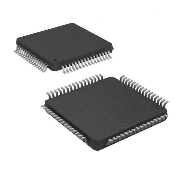


 工商网监
湘ICP备2023018690号
工商网监
湘ICP备2023018690号
