To our customers,
Old Company Name in Catalogs and Other Documents
On April 1st, 2010, NEC Electronics Corporation merged with Renesas Technology
Corporation, and Renesas Electronics Corporation took over all the business of both
companies. Therefore, although the old company name remains in this document, it is a valid
Renesas Electronics document. We appreciate your understanding.
Renesas Electronics website: http://www.renesas.com
April 1st, 2010
Renesas Electronics Corporation
Issued by: Renesas Electronics Corporation (http://www.renesas.com)
Send any inquiries to http://www.renesas.com/inquiry.
�Notice
1.
2.
3.
4.
5.
6.
7.
All information included in this document is current as of the date this document is issued. Such information, however, is
subject to change without any prior notice. Before purchasing or using any Renesas Electronics products listed herein, please
confirm the latest product information with a Renesas Electronics sales office. Also, please pay regular and careful attention to
additional and different information to be disclosed by Renesas Electronics such as that disclosed through our website.
Renesas Electronics does not assume any liability for infringement of patents, copyrights, or other intellectual property rights
of third parties by or arising from the use of Renesas Electronics products or technical information described in this document.
No license, express, implied or otherwise, is granted hereby under any patents, copyrights or other intellectual property rights
of Renesas Electronics or others.
You should not alter, modify, copy, or otherwise misappropriate any Renesas Electronics product, whether in whole or in part.
Descriptions of circuits, software and other related information in this document are provided only to illustrate the operation of
semiconductor products and application examples. You are fully responsible for the incorporation of these circuits, software,
and information in the design of your equipment. Renesas Electronics assumes no responsibility for any losses incurred by
you or third parties arising from the use of these circuits, software, or information.
When exporting the products or technology described in this document, you should comply with the applicable export control
laws and regulations and follow the procedures required by such laws and regulations. You should not use Renesas
Electronics products or the technology described in this document for any purpose relating to military applications or use by
the military, including but not limited to the development of weapons of mass destruction. Renesas Electronics products and
technology may not be used for or incorporated into any products or systems whose manufacture, use, or sale is prohibited
under any applicable domestic or foreign laws or regulations.
Renesas Electronics has used reasonable care in preparing the information included in this document, but Renesas Electronics
does not warrant that such information is error free. Renesas Electronics assumes no liability whatsoever for any damages
incurred by you resulting from errors in or omissions from the information included herein.
Renesas Electronics products are classified according to the following three quality grades: “Standard”, “High Quality”, and
“Specific”. The recommended applications for each Renesas Electronics product depends on the product’s quality grade, as
indicated below. You must check the quality grade of each Renesas Electronics product before using it in a particular
application. You may not use any Renesas Electronics product for any application categorized as “Specific” without the prior
written consent of Renesas Electronics. Further, you may not use any Renesas Electronics product for any application for
which it is not intended without the prior written consent of Renesas Electronics. Renesas Electronics shall not be in any way
liable for any damages or losses incurred by you or third parties arising from the use of any Renesas Electronics product for an
application categorized as “Specific” or for which the product is not intended where you have failed to obtain the prior written
consent of Renesas Electronics. The quality grade of each Renesas Electronics product is “Standard” unless otherwise
expressly specified in a Renesas Electronics data sheets or data books, etc.
“Standard”:
8.
9.
10.
11.
12.
Computers; office equipment; communications equipment; test and measurement equipment; audio and visual
equipment; home electronic appliances; machine tools; personal electronic equipment; and industrial robots.
“High Quality”: Transportation equipment (automobiles, trains, ships, etc.); traffic control systems; anti-disaster systems; anticrime systems; safety equipment; and medical equipment not specifically designed for life support.
“Specific”:
Aircraft; aerospace equipment; submersible repeaters; nuclear reactor control systems; medical equipment or
systems for life support (e.g. artificial life support devices or systems), surgical implantations, or healthcare
intervention (e.g. excision, etc.), and any other applications or purposes that pose a direct threat to human life.
You should use the Renesas Electronics products described in this document within the range specified by Renesas Electronics,
especially with respect to the maximum rating, operating supply voltage range, movement power voltage range, heat radiation
characteristics, installation and other product characteristics. Renesas Electronics shall have no liability for malfunctions or
damages arising out of the use of Renesas Electronics products beyond such specified ranges.
Although Renesas Electronics endeavors to improve the quality and reliability of its products, semiconductor products have
specific characteristics such as the occurrence of failure at a certain rate and malfunctions under certain use conditions. Further,
Renesas Electronics products are not subject to radiation resistance design. Please be sure to implement safety measures to
guard them against the possibility of physical injury, and injury or damage caused by fire in the event of the failure of a
Renesas Electronics product, such as safety design for hardware and software including but not limited to redundancy, fire
control and malfunction prevention, appropriate treatment for aging degradation or any other appropriate measures. Because
the evaluation of microcomputer software alone is very difficult, please evaluate the safety of the final products or system
manufactured by you.
Please contact a Renesas Electronics sales office for details as to environmental matters such as the environmental
compatibility of each Renesas Electronics product. Please use Renesas Electronics products in compliance with all applicable
laws and regulations that regulate the inclusion or use of controlled substances, including without limitation, the EU RoHS
Directive. Renesas Electronics assumes no liability for damages or losses occurring as a result of your noncompliance with
applicable laws and regulations.
This document may not be reproduced or duplicated, in any form, in whole or in part, without prior written consent of Renesas
Electronics.
Please contact a Renesas Electronics sales office if you have any questions regarding the information contained in this
document or Renesas Electronics products, or if you have any other inquiries.
(Note 1) “Renesas Electronics” as used in this document means Renesas Electronics Corporation and also includes its majorityowned subsidiaries.
(Note 2) “Renesas Electronics product(s)” means any product developed or manufactured by or for Renesas Electronics.
�To all our customers
Regarding the change of names mentioned in the document, such as Mitsubishi
Electric and Mitsubishi XX, to Renesas Technology Corp.
The semiconductor operations of Hitachi and Mitsubishi Electric were transferred to Renesas
Technology Corporation on April 1st 2003. These operations include microcomputer, logic, analog
and discrete devices, and memory chips other than DRAMs (flash memory, SRAMs etc.)
Accordingly, although Mitsubishi Electric, Mitsubishi Electric Corporation, Mitsubishi
Semiconductors, and other Mitsubishi brand names are mentioned in the document, these names
have in fact all been changed to Renesas Technology Corp. Thank you for your understanding.
Except for our corporate trademark, logo and corporate statement, no changes whatsoever have been
made to the contents of the document, and these changes do not constitute any alteration to the
contents of the document itself.
Note : Mitsubishi Electric will continue the business operations of high frequency & optical devices
and power devices.
Renesas Technology Corp.
Customer Support Dept.
April 1, 2003
�Mitsubishi microcomputers
M16C / 62M Group
(Low voltage version)
Description
SINGLE-CHIP 16-BIT CMOS MICROCOMPUTER
Description
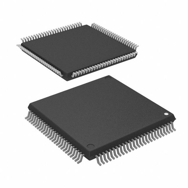
The M16C/62M group of single-chip microcomputers are built using the high-performance silicon gate
CMOS process using a M16C/60 Series CPU core and are packaged in a 100-pin plastic molded QFP.
These single-chip microcomputers operate using sophisticated instructions featuring a high level of instruction efficiency. With 1M bytes of address space, low voltage (2.2V to 3.6V), they are capable of executing
instructions at high speed. They also feature a built-in multiplier and DMAC, making them ideal for controlling office, communications, industrial equipment, and other high-speed processing applications.
The M16C/62M group includes a wide range of products with different internal memory types and sizes and
various package types.
Features
• Memory capacity .................................. ROM (See Figure 1.1.4. ROM Expansion)
RAM 10K to 20K bytes
• Shortest instruction execution time ...... 100ns (f(XIN)=10MHZ, VCC=2.7V to 3.6V)
142.9ns (f(XIN)=7MHZ, VCC=2.2V to 3.6V with software one-wait)
• Supply voltage ..................................... 2.7V to 3.6V (f(XIN)=10MHZ, without software wait)
2.4V to 2.7V (f(XIN)=7MHZ, without software wait)
2.2V to 2.4V (f(XIN)=7MHZ with software one-wait)
• Low power consumption ...................... 28.5mW (VCC = 3V, f(XIN)=10MHZ, without software wait)
• Interrupts .............................................. 25 internal and 8 external interrupt sources, 4 software
interrupt sources; 7 levels (including key input interrupt)
• Multifunction 16-bit timer ...................... 5 output timers + 6 input timers
• Serial I/O .............................................. 5 channels
(3 for UART or clock synchronous, 2 for clock synchronous)
• DMAC .................................................. 2 channels (trigger: 24 sources)
• A-D converter ....................................... 10 bits X 8 channels (Expandable up to 10 channels)
• D-A converter ....................................... 8 bits X 2 channels
• CRC calculation circuit ......................... 1 circuit
• Watchdog timer .................................... 1 line
• Programmable I/O ............................... 87 lines
_______
• Input port .............................................. 1 line (P85 shared with NMI pin)
• Memory expansion .............................. Available (to a maximum of 1M bytes)
• Chip select output ................................ 4 lines
• Clock generating circuit ....................... 2 built-in clock generation circuits
(built-in feedback resistor, and external ceramic or quartz oscillator)
Applications
Audio, cameras, office equipment, communications equipment, portable equipment
1
�Mitsubishi microcomputers
M16C / 62M Group
(Low voltage version)
Description
SINGLE-CHIP 16-BIT CMOS MICROCOMPUTER
Pin Configuration
Figures 1.1.1 and 1.1.2 show the pin configurations (top view).
P10/D8
P11/D9
P12/D10
P13/D11
P14/D12
P15/D13/INT3
P16/D14/INT4
P17/D15/INT5
P20/A0(/D0/-)
P21/A1(/D1/D0)
P22/A2(/D2/D1)
P23/A3(/D3/D2)
P24/A4(/D4/D3)
P25/A5(/D5/D4)
P26/A6(/D6/D5)
P27/A7(/D7/D6)
Vss
P30/A8(/-/D7)
Vcc
P31/A9
P32/A10
P33/A11
P34/A12
P35/A13
P36/A14
P37/A15
P40/A16
P41/A17
P42/A18
P43/A19
PIN CONFIGURATION (top view)
80 79 78 77 76 75 74 73 72 71 70 69 68 67 66 65 64 63 62 61 60 59 58 57 56 55 54 53 52 51
P07/D7
P06/D6
P05/D5
P04/D4
P03/D3
P02/D2
P01/D1
P00/D0
P107/AN7/KI3
P106/AN6/KI2
P105/AN5/KI1
P104/AN4/KI0
P103/AN3
P102/AN2
P101/AN1
AVSS
P100/AN0
VREF
AVcc
P97/ADTRG/SIN4
81
82
83
84
85
86
87
88
89
90
91
92
93
94
95
96
97
98
99
M16C/62M group
(Low voltage version)
100
2 3
4 5
P44/CS0
P45/CS1
P46/CS2
P47/CS3
P50/WRL/WR
P51/WRH/BHE
P52/RD
P53/BCLK
P54/HLDA
P55/HOLD
P56/ALE
P57/RDY/CLKOUT
P60/CTS0/RTS0
P61/CLK0
P62/RxD0
P63/TXD0
P64/CTS1/RTS1/CLKS1
P65/CLK1
P66/RxD1
P67/TXD1
6 7 8 9 10 11 12 13 14 15 16 17 18 19 20 21 22 23 24 25 26 27 28 29 30
P96/ANEX1/SOUT4
P95/ANEX0/CLK4
P94/DA1/TB4IN
P93/DA0/TB3IN
P92/TB2IN/SOUT3
P91/TB1IN/SIN3
P90/TB0IN/CLK3
BYTE
CNVss
P87/XCIN
P86/XCOUT
RESET
XOUT
VSS
XIN
VCC
P85/NMI
P84/INT2
P83/INT1
P82/INT0
P81/TA4IN/U
P80/TA4OUT/U
P77/TA3IN
P76/TA3OUT
P75/TA2IN/W
P74/TA2OUT/W
P73/CTS2/RTS2/TA1IN/V
P72/CLK2/TA1OUT/V
P71/RxD2/SCL/TA0IN/TB5IN
P70/TXD2/SDA/TA0OUT
1
50
49
48
47
46
45
44
43
42
41
40
39
38
37
36
35
34
33
32
31
Package: 100P6S-A
Figure 1.1.1. Pin configuration (top view)
2
�Mitsubishi microcomputers
M16C / 62M Group
(Low voltage version)
Description
SINGLE-CHIP 16-BIT CMOS MICROCOMPUTER
P13/D11
P14/D12
P15/D13/INT3
P16/D14/INT4
P17/D15/INT5
P20/A0(/D0/-)
P21/A1(/D1/D0)
P22/A2(/D2/D1)
P23/A3(/D3/D2)
P24/A4(/D4/D3)
P25/A5(/D5/D4)
P26/A6(/D6/D5)
P27/A7(/D7/D6)
Vss
P30/A8(/-/D7)
Vcc
P31/A9
P32/A10
P33/A11
P34/A12
P35/A13
P36/A14
P37/A15
P40/A16
P41/A17
PIN CONFIGURATION (top view)
75 74 73 72 71 70 69 68 67 66 65 64 63 62 61 60 59 58 57 56 55 54 53 52 51
P12/D10
P11/D9
P10/D8
P07/D7
P06/D6
P05/D5
P04/D4
P03/D3
P02/D2
P01/D1
P00/D0
P107/AN7/KI3
P106/AN6/KI2
P105/AN5/KI1
P104/AN4/KI0
P103/AN3
P102/AN2
P101/AN1
AVSS
P100/AN0
VREF
AVcc
P97/ADTRG/SIN4
P96/ANEX1/SOUT4
P95/ANEX0/CLK4
76
77
78
79
80
50
49
48
47
46
45
44
81
82
83
84
85
86
M16C/62M group
(Low voltage version)
87
88
89
90
91
92
93
94
95
96
43
42
41
40
39
38
37
36
35
34
33
32
31
30
29
97
98
99
100
28
27
26
3 4 5 6 7
8 9 10 11 12 13 14 15 16 17 18 19 20 21 22 23 24 25
P94/DA1/TB4IN
P93/DA0/TB3IN
P92/TB2IN/SOUT3
P91/TB1IN/SIN3
P90/TB0IN/CLK3
BYTE
CNVss
P87/XCIN
P86/XCOUT
RESET
XOUT
VSS
XIN
VCC
P85/NMI
P84/INT2
P83/INT1
P82/INT0
P81/TA4IN/U
P80/TA4OUT/U
P77/TA3IN
P76/TA3OUT
P75/TA2IN/W
P74/TA2OUT/W
P73/CTS2/RTS2/TA1IN/V
1 2
P42/A18
P43/A19
P44/CS0
P45/CS1
P46/CS2
P47/CS3
P50/WRL/WR
P51/WRH/BHE
P52/RD
P53/BCLK
P54/HLDA
P55/HOLD
P56/ALE
P57/RDY/CLKOUT
P60/CTS0/RTS0
P61/CLK0
P62/RxD0
P63/TXD0
P64/CTS1/RTS1/CLKS1
P65/CLK1
P66/RxD1
P67/TXD1
P70/TXD2/SDA/TA0OUT
P71/RxD2/SCL/TA0IN/TB5IN
P72/CLK2/TA1OUT/V
Package: 100P6Q-A
Figure 1.1.2. Pin configuration (top view)
3
�Mitsubishi microcomputers
M16C / 62M Group
(Low voltage version)
Description
SINGLE-CHIP 16-BIT CMOS MICROCOMPUTER
Block Diagram
Figure 1.1.3 is a block diagram of the M16C/62M group.
8
I/O ports
Port P0
8
8
Port P1
Port P2
8
Port P3
Port P4
Port P5
UART/clock synchronous SI/O
Clock synchronous SI/O
(8 bits X 3 channels)
(8 bits X 2 channels)
Registers
(15 bits)
(2 channels)
(8 bits X 2 channels)
Note 1: ROM size depends on MCU type.
Note 2: RAM size depends on MCU type.
Figure 1.1.3. Block diagram of M16C/62M group
ISP
USP
Flag register
FLG
Multiplier
8
SB
INTB
Stack pointer
RAM
(Note 2)
Port P10
D-A converter
PC
Vector table
ROM
(Note 1)
8
DMAC
Program counter
Memory
Port P9
Watchdog timer
R0H
R0L
R0H
R0L
R1H
R1L
R1H
R1L
R2
R2
R3
R3
A0
A0
A1
A1
FB
FB
AAAAAA
AAAAAA
AAAAAA
AAAAAA
AAAAAA
AAAA
AAAA
Port P85
M16C/60 series16-bit CPU core
7
XIN-XOUT
XCIN-XCOUT
8
Expandable up to 10 channels)
Port P8
System clock generator
(10 bits X 8 channels
Port P6
Port P7
A-D converter
Timer
CRC arithmetic circuit (CCITT )
(Polynomial : X16+X12+X5+1)
8
8
Internal peripheral functions
Timer TA0 (16 bits)
Timer TA1 (16 bits)
Timer TA2 (16 bits)
Timer TA3 (16 bits)
Timer TA4 (16 bits)
Timer TB0 (16 bits)
Timer TB1 (16 bits)
Timer TB2 (16 bits)
Timer TB3 (16 bits)
Timer TB4 (16 bits)
Timer TB5 (16 bits)
4
8
�Mitsubishi microcomputers
M16C / 62M Group
(Low voltage version)
Description
SINGLE-CHIP 16-BIT CMOS MICROCOMPUTER
Performance Outline
Table 1.1.1 is a performance outline of M16C/62M group.
Table 1.1.1. Performance outline of M16C/62M group
Item
Number of basic instructions
Shortest instruction execution time
Performance
91 instructions
100ns(f(XIN)=10MHZ, VCC=2.7V to 3.6V)
142.9ns (f(XIN)=7MHZ, VCC=2.2V to 3.6V with software one-wait)
Memory
ROM
(See the figure 1.1.4. ROM Expansion)
capacity
RAM
10K to 20K bytes
I/O port
P0 to P10 (except P85)
8 bits x 10, 7 bits x 1
Input port
P85
1 bit x 1
Multifunction TA0, TA1, TA2, TA3, TA4
16 bits x 5
timer
TB0, TB1, TB2, TB3, TB4, TB5 16 bits x 6
Serial I/O
UART0, UART1, UART2
(UART or clock synchronous) x 3
SI/O3, SI/O4
(Clock synchronous) x 2
A-D converter
D-A converter
DMAC
CRC calculation circuit
Watchdog timer
Interrupt
Clock generating circuit
Supply voltage
Power consumption
I/O
I/O withstand voltage
characteristics Output current
Memory expansion
Device configuration
Package
10 bits x (8 + 2) channels
8 bits x 2
2 channels (trigger: 24 sources)
CRC-CCITT
15 bits x 1 (with prescaler)
25 internal and 8 external sources, 4 software sources, 7 levels
2 built-in clock generation circuits
(built-in feedback resistor, and external ceramic or quartz oscillator)
2.7V to 3.6V (f(XIN)=10MHZ, without software wait)
2.4V to 2.7V (f(XIN)=7MHZ, without software wait)
2.2V to 2.4V (f(XIN)=7MHZ with software one-wait)
28.5mW (f(XIN) =10MHZ, VCC=3V without software wait)
3V
1mA
Available (to a maximum of 1M bytes)
CMOS high performance silicon gate
100-pin plastic mold QFP
5
�Mitsubishi microcomputers
M16C / 62M Group
(Low voltage version)
Description
SINGLE-CHIP 16-BIT CMOS MICROCOMPUTER
Mitsubishi plans to release the following products in the M16C/62M group:
(1) Support for mask ROM version and Flash memory version
(2) ROM capacity
(3) Package
100P6S-A : Plastic molded QFP (mask ROM and flash memory versions)
100P6Q-A : Plastic molded QFP (mask ROM and flash memory versions)
ROM Size
(Byte)
External
ROM
256K
M30624MGM-XXXFP/GP
M30624FGMFP/GP
128K
M30620MCM-XXXFP/GP
M30620FCMFP/GP
96K
64K
32K
Mask ROM version
Flash memory version
Figure 1.1.4. ROM expansion
The M16C/62M group products currently supported are listed in Table 1.1.2.
Table 1.1.2. M16C/62M group
Type No
M30620MCM-XXXFP
M30620MCM-XXXGP
M30624MGM-XXXFP
M30624MGM-XXXGP
M30620FCMFP
M30620FCMGP
June, 2001
ROM capacity
RAM capacity
128K byte
10K byte
256K byte
20K byte
128K byte
10K byte
6
100P6S-A
100P6Q-A
100P6S-A
mask ROM version
100P6Q-A
100P6Q-A
100P6S-A
256K byte
Remarks
100P6S-A
M30624FGMFP
M30624FGMGP
Package type
20K byte
100P6Q-A
Flash memory
3V version
�Mitsubishi microcomputers
M16C / 62M Group
(Low voltage version)
Description
SINGLE-CHIP 16-BIT CMOS MICROCOMPUTER
Type No. M 3 0 6 2 0 M C M – X X X F P
Package type:
FP : Package
GP :
100P6S-A
100P6Q-A
ROM No.
Omitted for blank flash memory version
ROM capacity:
C : 128K bytes
G : 256K bytes
Memory type:
M : Mask ROM version
F : Flash memory version
Shows RAM capacity, pin count, etc
(The value itself has no specific meaning)
M16C/62 Group
M16C Family
Figure 1.1.5. Type No., memory size, and package
7
�Mitsubishi microcomputers
M16C / 62M Group
(Low voltage version)
Electrical characteristics
SINGLE-CHIP 16-BIT CMOS MICROCOMPUTER
Table 1.26.1. Absolute maximum ratings
Symbol
Vcc
AVcc
Parameter
Condition
- 0.3 to 4.6
V
Analog supply voltage
VCC=AVCC
- 0.3 to 4.6
V
- 0.3 to Vcc + 0.3
V
- 0.3 to 4.6
V
- 0.3 to Vcc + 0.3
V
- 0.3 to 4.6
300
- 20 to 85 / -40 to 85 (Note)
V
mW
C
- 65 to 150
C
VI
RESET, CNVSS, BYTE,
P00 to P07, P10 to P17, P20 to P27,
P30 to P37,P40 to P47, P50 to P57,
P60 to P67, P72 to P77, P80 to P87,
P90 to P97, P100 to P107,
VREF, XIN
P70, P71
Output
voltage
Pd
P00 to P07, P10 to P17, P20 to P27,
P30 to P37, P40 to P47, P50 to P57,
P60 to P67, P72 to P77, P80 to P84,
P86, P87, P90 to P97, P100 to P107,
XOUT
P70, P71
Power dissipation
Operating ambient temperature
Topr
Storage temperature
Tstg
Note : Specify a product of -40°C to 85°C to use it.
8
Unit
VCC=AVCC
Input
voltage
VO
Rated value
Supply voltage
Topr=25 C
�Mitsubishi microcomputers
M16C / 62M Group
(Low voltage version)
Electrical characteristics
SINGLE-CHIP 16-BIT CMOS MICROCOMPUTER
Table 1.26.2. Recommended operating conditions (referenced to VCC = 2.2V to 3.6V at Topr =
–20°C to 85oC / – 40°C to 85oC (Note 3) unless otherwise specified)
Parameter
Symbol
Min.
Supply voltage
Analog supply voltage
Supply voltage
Analog supply voltage
Vcc
AVcc
Vss
AVss
HIGH input
voltage
Standard
Typ.
2.2
P31 to P37, P40 to P47, P50 to P57, P60 to P67,
P72 to P77, P80 to P87, P90 to P97, P100 to P107,
XIN, RESET, CNVSS, BYTE
P70, P71
P00 to P07, P10 to P17, P20 to P27, P30 (during single-chip mode)
P00 to P07, P10 to P17, P20 to P27, P30
3.0
Vcc
Max.
3.6
Unit
V
0
V
V
0
V
0.8Vcc
Vcc
V
0.8Vcc
4.6
Vcc
V
0.8Vcc
0.5Vcc
Vcc
V
0
0.2Vcc
V
0
0.2Vcc
V
0
0.16Vcc
V
HIGH peak output
I OH (peak) current
- 10.0
mA
I OH (avg)
- 5.0
mA
10.0
mA
5.0
mA
0
10
MHz
0
10 X Vcc
- 17
17.5 X Vcc
- 35
10
MHz
VIH
(data input function during memory expansion and microprocessor modes)
LOW input
voltage
VIL
P31 to P37, P40 to P47, P50 to P57, P60 to P67,
P70 to P77, P80 to P87, P90 to P97, P100 to P107,
XIN, RESET, CNVSS, BYTE
P00 to P07, P10 to P17, P20 to P27, P30 (during single-chip mode)
P00 to P07, P10 to P17, P20 to P27, P30
(data input function during memory expansion and microprocessor modes)
I OL (peak)
I OL (avg)
P00 to P07, P10 to P17, P20 to P27, P30 to P37,
P40 to P47, P50 to P57, P60 to P67, P72 to P77,
P80 to P84, P86, P87, P90 to P97, P100 to P107
HIGH average output P00 to P07, P10 to P17, P20 to P27, P30 to P37,
P40 to P47, P50 to P57, P60 to P67, P72 to P77,
current
P80 to P84, P86, P87, P90 to P97, P100 to P107
P00 to P07, P10 to P17, P20 to P27, P30 to P37,
LOW peak output
P40 to P47, P50 to P57, P60 to P67, P70 to P77,
current
P80 to P84, P86, P87, P90 to P97, P100 to P107
P00 to P07, P10 to P17, P20 to P27, P30 to P37,
LOW average
P40 to P47, P50 to P57, P60 to P67, P70 to P77,
output current
P80 to P84, P86, P87, P90 to P97, P100 to P107
Vcc=2.7V to 3.6V
No wait
f (XIN)
Main clock input
oscillation
frequency
f (XcIN)
Vcc=2.4V to 2.7V
with wait
Vcc=2.2V to 2.4V
0
Vcc=2.7V to 3.6V
0
Vcc=2.2V to 2.7V
0
6 X Vcc
- 6.2
Subclock oscillation frequency
32.768
50
V
MHz
MHz
MHz
kHz
Note 1: The mean output current is the mean value within 100ms.
Note 2: The total IOL (peak) for ports P0, P1, P2, P86, P87, P9, and P10 must be 80mA max. The total IOH (peak) for ports P0, P1,
P2, P86, P87, P9, and P10 must be 80mA max. The total IOL (peak) for ports P3, P4, P5, P6, P7, and P80 to P84 must be
80mA max. The total IOH (peak) for ports P3, P4, P5, P6, P72 to P77, and P80 to P84 must be 80mA max.
Note 3: Specify a product of -40°C to 85°C to use it.
Note 4: Relationship between main clock oscillation frequency and supply voltage.
10.0
7.0
AAAAAAA
AAAAAAA
AAAAAAA
AAAAAAA
AAAAAAA
AAAAAAA
AAAAAAA
AAAAAAA
10 X VCC –17MHZ
17.5 X VCC
–35MHZ
3.5
0.0
2.2
2.4
2.7
Supply voltage[V]
(BCLK: no division)
3.6
Main clock input oscillation frequency
(With wait)
Operating maximum frequency [MHZ]
Operating maximum frequency [MHZ]
Main clock input oscillation frequency
(No wait)
10.0
7.0
0.0
AAAAAAA
AAAAAAA
AAAAAAA
AAAAAAA
AAAAAAA
AAAAAAA
AAAAAAA
AAAAAAA
Flash memory version program voltage and read
operation voltage characteristics
6 X VCC –6.2MHZ
2.2
2.4
2.7
Flash program voltage
Flash read operation voltage
VCC=2.7V to 3.6V
VCC=2.4V to 3.6V
VCC=2.7V to 3.4V
VCC=2.2V to 2.4V
3.6
Supply voltage[V]
(BCLK: no division)
Note 5: Execute case without wait, program / erase of flash memory by VCC=2.7V to 3.6V and f(BCLK) ≤ 6.25 MHz. Execute case
with wait, program / erase of flash memory by VCC=2.7V to 3.6V and f(BCLK) ≤ 10.0 MHz.
9
�Mitsubishi microcomputers
M16C / 62M Group
(Low voltage version)
Electrical characteristics
SINGLE-CHIP 16-BIT CMOS MICROCOMPUTER
Table 1.26.3. Electrical characteristics (referenced to VCC = 2.7V to 3.6V, VSS = 0V at Topr = – 20oC to
85oC / – 40oC to 85oC (Note 1), f(XIN) = 10MHZ without wait unless otherwise specified)
VOH
VOH
VOL
VOL
Measuring condition
Parameter
Symbol
HIGH output
voltage
P00 to P07, P10 to P17, P20 to P27, P30 to P37,
P40 to P47, P50 to P57, P60 to P67, P72 to P77,
P80 to P84, P86,P87, P90 to P97, P100 to P107
HIGH output
voltage
XOUT
HIGH output
voltage
XCOUT
2.5
HIGHPOWER
IOH=–0.1mA
2.5
LOWPOWER
IOH=–50µA
2.5
HIGHPOWER
With no load applied
3.0
LOWPOWER
With no load applied
1.6
P00 to P07, P10 to P17, P20 to P27, P30 to P37,
P40 to P47, P50 to P57, P60 to P67, P70 to P77,
P80 to P84, P86,P87, P90 to P97, P100 to P107
LOW output
voltage
XOUT
Hysteresis
VT+–VT–
XCOUT
Standard
Unit
Typ. Max.
IOH=–1mA
LOW output
voltage
LOW output
voltage
Min
V
V
V
IOL=1mA
0 .5
HIGHPOWER
IOL=0.1mA
0 .5
LOWPOWER
IOL=50µA
HIGHPOWER
With no load applied
0
LOWPOWER
With no load applied
0
0 .5
V
V
V
HOLD, RDY, TA0IN to TA4IN, TB0IN to TB5IN,
INT0 to INT5, NMI, ADTRG, CTS0 to CTS2, SCL,
SDA, CLK0 to CLK4, TA2OUT to TA4OUT,
KI0 to KI3, RxD0 to RxD2, SIN3, SIN4
0.2
0 .8
V
0.2
1 .8
V
VT+–VT–
Hysteresis
RESET
IIH
HIGH input
current
P00 to P07, P10 to P17, P20 to P27, P30 to P37,
P40 to P47, P50 to P57, P60 to P67, P70 to P77,
P80 to P87, P90 to P97, P100 to P107,
XIN, RESET, CNVss, BYTE
VI=3V
4 .0
µA
IIL
LOW input
current
P00 to P07, P10 to P17, P20 to P27, P30 to P37,
P40 to P47, P50 to P57, P60 to P67, P70 to P77,
P80 to P87, P90 to P97, P100 to P107,
XIN, RESET, CNVss, BYTE
VI=0V
–4.0
µA
RPULLUP
Pull-up
resistance
330
kΩ
P00 to P07, P10 to P17, P20 to P27, P30 to P37,
P40 to P47, P50 to P57, P60 to P67, P72 to P77,
P80 to P84, P86,P87, P90 to P97, P100 to P107
VI=0V
20
75
RfXIN
Feedback resistance
XIN
3 .0
MΩ
RfXCIN
Feedback resistance
XCIN
10.0
MΩ
VRAM
RAM retention voltage
When clock is stopped
Mask ROM version
In single-chip mode, the output pins
are open and other pins are VSS
Flash memory
3V version
program
ICC
Power supply current
Flash memory
3V version
erase
V
f(XIN)=10MHz
Square wave,
no division
9 .5
21.25
mA
12.0
21.25
mA
f(XIN)=10MHz
Square wave,
no division
Mask ROM version, f(XCIN)=32kHz
flash memory
Square wave
3V version
Flash memory
3V version
2.0
45.0
µA
14.0
mA
17.0
mA
2 .8
µA
0 .9
µA
f(XIN)=10MHz
Square wave,
division by 2
f(XIN)=10MHz
Square wave,
division by 2
Mask ROM version, f(XCIN)=32kHz
When a WAIT instruction
flash memory
is executed.
3V version
Oscillation capacity High
(Note 2)
f(XCIN)=32kHz
When a WAIT instruction
is executed.
Oscillation capacity Low
(Note 2)
When clock is stopped
Topr=25°C
1.0
µA
When clock is stopped
Topr=85°C
Note 1: Specify a product of -40°C to 85°C to use it.
Note 2: With one timer operated using fC32.
10
20.0
�Mitsubishi microcomputers
M16C / 62M Group
(Low voltage version)
Electrical characteristics
SINGLE-CHIP 16-BIT CMOS MICROCOMPUTER
Table 1.26.4. A-D conversion characteristics (referenced to VCC = AVCC = VREF = 2.4V to 3.6V, VSS = AVSS
= 0V, at Topr = – 20oC to 85oC / – 40oC to 85oC (Note 2), f(XIN)=10MHZ unless otherwise specified)
Standard
Symbol
Parameter
Measuring condition
Unit
Min. Typ. Max
–
Resolution
–
Absolute accuracy
Sample & hold function not available (8 bit)
RLADDER
tCONV
Ladder resistance
Conversion
time(8bit)
VREF
Reference voltage
VIA
Analog input voltage
VREF =VCC
10
Bits
VREF =VCC=3V, fAD=fAD/2
±2
LSB
40
kΩ
VREF =VCC
10
µs
9.8
2.4
VCC
V
0
VREF
V
Note 1: Connect AVCC pin to VCC pin and apply the same electric potential.
Note 2: Specify a product of –40°C to 85°C to use it.
Table 1.26.5. D-A conversion characteristics (referenced to VCC = 2.4V to 3.6V, VSS = AVSS = 0V, VREF=3V,
at Topr = – 20oC to 85oC / – 40oC to 85oC (Note 2), f(XIN)=10MHZ unless otherwise specified)
Standard
Parameter
Measuring condition
Unit
Min. Typ. Max
Symbol
–
–
tsu
RO
IVREF
Resolution
Absolute accuracy
Setup time
4
Output resistance
Reference power supply input current
10
(Note1)
8
1.0
3
20
Bits
%
µs
kΩ
1.0
mA
Note 1: This applies when using one D-A converter, with the D-A register for the unused D-A converter set to “0016”.
The A-D converter's ladder resistance is not included.
Also, when D-A register contents are not “0016”, the current IVREF always flows even though Vref may have
been set to be “unconnected” by the A-D control register.
Note 2: Specify a product of –40°C to 85°C to use it.
Table 1.26.6. Flash memory version electrical characteristics
(referenced to VCC = 2.7V to 3.6V, at Topr = 0oC to 60oC unless otherwise specified)
Standard
Parameter
Min.
Typ.
Max
Page program time
6
Block erase time
Erase all unlocked blocks time
Lock bit program time
Unit
120
ms
50
600
ms
50 X n (Note)
600 X n (Note)
ms
120
ms
6
Note : n denotes the number of block erases.
Table 1.26.7. Flash memory version program voltage and read operation voltage characteristics
(Topr = 0oC to 60oC)
Flash program voltage
Flash read operation voltage
VCC=2.7V to 3.6V
VCC=2.4V to 3.6V
VCC=2.7V to 3.4V
VCC=2.2V to 2.4V
11
�Mitsubishi microcomputers
M16C / 62M Group
(Low voltage version)
Timing
SINGLE-CHIP 16-BIT CMOS MICROCOMPUTER
Timing requirements
(referenced to VCC = 3V, VSS = 0V, at Topr = – 20oC to 85oC / – 40oC to 85oC (*) unless otherwise specified)
* : Specify a product of -40°C to 85°C to use it.
Table 1.26.8. External clock input
Standard
Parameter
Symbol
tc
External clock input cycle time
External clock input HIGH pulse width
External clock input LOW pulse width
tw(H)
tw(L)
tr
Min.
Unit
ns
100
40
ns
40
ns
External clock rise time
External clock fall time
tf
Max.
18
ns
18
ns
Table 1.26.9. Memory expansion and microprocessor modes
Symbol
tac1(RD-DB)
tac2(RD-DB)
tac3(RD-DB)
tsu(DB-RD)
tsu(RDY-BCLK )
tsu(HOLD-BCLK )
th(RD-DB)
th(BCLK -RDY)
th(BCLK-HOLD )
td(BCLK-HLDA)
Parameter
Data input access time (no wait)
(Note)
Data input access time (with wait)
Data input access time (when accessing multiplex bus area)
Data input setup time
RDY input setup time
HOLD input setup time
Data input hold time
RDY input hold time
HOLD input hold time
HLDA output delay time
(Note)
Note: Calculated according to the BCLK frequency as follows:
tac1(RD – DB) =
10 9
– 90
f(BCLK) X 2
tac2(RD – DB) =
3 X 10
– 90
f(BCLK) X 2
[ns]
tac3(RD – DB) =
3 X 10 9
– 90
f(BCLK) X 2
[ns]
[ns]
9
12
Standard
Min.
Max.
(Note)
80
60
Unit
ns
ns
ns
ns
ns
ns
80
0
ns
ns
0
0
ns
100
ns
�Mitsubishi microcomputers
M16C / 62M Group
(Low voltage version)
Timing
SINGLE-CHIP 16-BIT CMOS MICROCOMPUTER
Timing requirements
(referenced to VCC = 3V, VSS = 0V, at Topr = – 20oC to 85oC / – 40oC to 85oC (*) unless otherwise specified)
* : Specify a product of –40°C to 85°C to use it.
Table 1.26.10. Timer A input (counter input in event counter mode)
Symbol
Parameter
tc(TA)
TAiIN input cycle time
tw(TAH)
tw(TAL)
TAiIN input HIGH pulse width
TAiIN input LOW pulse width
Standard
Min.
150
Max.
Unit
ns
60
60
ns
ns
Table 1.26.11. Timer A input (gating input in timer mode)
Standard
Symbol
Parameter
Min.
Max.
Unit
tc(TA)
TAiIN input cycle time
600
ns
tw(TAH)
tw(TAL)
TAiIN input HIGH pulse width
TAiIN input LOW pulse width
300
300
ns
ns
Table 1.26.12. Timer A input (external trigger input in one-shot timer mode)
Symbol
Parameter
Standard
Min.
Max.
Unit
tc(TA)
TAiIN input cycle time
300
ns
tw(TAH)
tw(TAL)
TAiIN input HIGH pulse width
TAiIN input LOW pulse width
150
150
ns
ns
Table 1.26.13. Timer A input (external trigger input in pulse width modulation mode)
Symbol
Parameter
tw(TAH)
TAiIN input HIGH pulse width
tw(TAL)
TAiIN input LOW pulse width
Standard
Min.
Max.
150
150
Unit
ns
ns
Table 1.26.14. Timer A input (up/down input in event counter mode)
Symbol
Parameter
Standard
Max.
Unit
tc(UP)
TAiOUT input cycle time
Min.
3000
tw(UPH)
TAiOUT input HIGH pulse width
1500
ns
tw(UPL)
TAiOUT input LOW pulse width
1500
ns
tsu(UP-TIN)
TAiOUT input setup time
600
ns
th(TIN-UP)
TAiOUT input hold time
600
ns
ns
13
�Mitsubishi microcomputers
M16C / 62M Group
(Low voltage version)
Timing
SINGLE-CHIP 16-BIT CMOS MICROCOMPUTER
Timing requirements
(referenced to VCC = 3V, VSS = 0V, at Topr = – 20oC to 85oC / – 40oC to 85oC (*) unless otherwise specified)
* : Specify a product of –40°C to 85°C to use it.
Table 1.26.15. Timer B input (counter input in event counter mode)
Parameter
Symbol
tc(TB)
tw(TBH)
TBiIN input cycle time (counted on one edge)
TBiIN input HIGH pulse width (counted on one edge)
Standard
Max.
Min.
Unit
150
60
ns
ns
60
ns
TBiIN input HIGH pulse width (counted on both edges)
300
160
ns
ns
TBiIN input LOW pulse width (counted on both edges)
160
ns
tw(TBL)
TBiIN input LOW pulse width (counted on one edge)
tc(TB)
tw(TBH)
TBiIN input cycle time (counted on both edges)
tw(TBL)
Table 1.26.16. Timer B input (pulse period measurement mode)
Parameter
Symbol
Standard
Unit
tc(TB)
TBiIN input cycle time
Min.
600
tw(TBH)
TBiIN input HIGH pulse width
300
ns
tw(TBL)
TBiIN input LOW pulse width
300
ns
Standard
Min.
Max.
Unit
Max.
ns
Table 1.26.17. Timer B input (pulse width measurement mode)
Parameter
Symbol
tc(TB)
TBiIN input cycle time
600
ns
tw(TBH)
tw(TBL)
TBiIN input HIGH pulse width
TBiIN input LOW pulse width
300
300
ns
ns
Standard
Min.
Max.
Unit
1500
200
ns
ns
Table 1.26.18. A-D trigger input
Symbol
tc(AD)
tw(ADL)
Parameter
ADTRG input cycle time (trigger able minimum)
ADTRG input LOW pulse width
Table 1.26.19. Serial I/O
Symbol
Parameter
tc(CK)
tw(CKH)
CLKi input cycle time
CLKi input HIGH pulse width
tw(CKL)
td(C-Q)
CLKi input LOW pulse width
TxDi output delay time
th(C-Q)
TxDi hold time
tsu(D-C)
th(C-D)
RxDi input setup time
RxDi input hold time
Standard
Min.
300
150
Max.
Unit
ns
ns
150
160
ns
ns
0
ns
50
90
ns
ns
_______
Table 1.26.20. External interrupt INTi inputs
Symbol
14
Parameter
Standard
tw(INH)
INTi input HIGH pulse width
Min.
380
tw(INL)
INTi input LOW pulse width
380
Max.
Unit
ns
ns
�Mitsubishi microcomputers
M16C / 62M Group
(Low voltage version)
Timing
SINGLE-CHIP 16-BIT CMOS MICROCOMPUTER
Switching characteristics (referenced to VCC = 3V, VSS = 0V at Topr = – 20oC to 85oC / – 40oC to
85oC (Note 3), CM15 = “1” unless otherwise specified)
Table 1.26.21. Memory expansion and microprocessor modes (with no wait)
Symbol
td(BCLK-AD)
th(BCLK-AD)
th(RD-AD)
th(WR-AD)
td(BCLK-CS)
th(BCLK-CS)
td(BCLK-ALE)
th(BCLK-ALE)
td(BCLK-RD)
th(BCLK-RD)
td(BCLK-WR)
th(BCLK-WR)
td(BCLK-DB)
th(BCLK-DB)
td(DB-WR)
th(WR-DB)
Measuring condition
Parameter
Address output delay time
Address output hold time (BCLK standard)
Address output hold time (RD standard)
Address output hold time (WR standard)
Chip select output delay time
Chip select output hold time (BCLK standard)
ALE signal output delay time
ALE signal output hold time
RD signal output delay time
RD signal output hold time
WR signal output delay time
WR signal output hold time
Data output delay time (BCLK standard)
Data output hold time (BCLK standard)
Data output delay time (WR standard)
Data output hold time (WR standard)(Note2)
Figure 1.26.1
Standard
Min.
Max.
60
4
0
0
60
4
60
–4
60
0
60
0
80
4
(Note1)
0
Unit
ns
ns
ns
ns
ns
ns
ns
ns
ns
ns
ns
ns
ns
ns
ns
ns
Note 1: Calculated according to the BCLK frequency as follows:
td(DB – WR) =
10 9
f(BCLK) X 2
– 80
[ns]
Note 2: This is standard value shows the timing when the output is off,
and doesn't show hold time of data bus.
Hold time of data bus is different by capacitor volume and pull-up
(pull-down) resistance value.
Hold time of data bus is expressed in
t = –CR X ln (1 – VOL / VCC)
by a circuit of the right figure.
For example, when VOL = 0.2VCC, C = 30pF, R = 1kΩ, hold time
of output “L” level is
t = – 30pF X 1kΩ X ln (1 – 0.2VCC / VCC)
= 6.7ns.
R
DBi
C
Note 3: Specify a product of –40°C to 85°C to use it.
P0
P1
P2
30pF
P3
P4
P5
P6
P7
P8
P9
P10
Figure 1.26.1. Port P0 to P10 measurement circuit
15
�Mitsubishi microcomputers
M16C / 62M Group
(Low voltage version)
Timing
SINGLE-CHIP 16-BIT CMOS MICROCOMPUTER
Switching characteristics (referenced to VCC = 3V, VSS = 0V at Topr = – 20oC to 85oC / – 40oC to
85oC (Note 3), CM15 = “1” unless otherwise specified)
Table 1.26.22. Memory expansion and microprocessor modes
(when accessing external memory area with wait)
Symbol
Measuring condition
Parameter
td(BCLK-AD)
th(BCLK-AD)
th(RD-AD)
Address output delay time
Address output hold time (BCLK standard)
Address output hold time (RD standard)
th(WR-AD)
td(BCLK-CS)
th(BCLK-CS)
td(BCLK-ALE)
Address output hold time (WR standard)
Chip select output delay time
Chip select output hold time (BCLK standard)
ALE signal output delay time
th(BCLK-ALE)
td(BCLK-RD)
th(BCLK-RD)
td(BCLK-WR)
th(BCLK-WR)
td(BCLK-DB)
th(BCLK-DB)
td(DB-WR)
ALE signal output hold time
RD signal output delay time
RD signal output hold time
WR signal output delay time
WR signal output hold time
Data output delay time (BCLK standard)
Data output hold time (BCLK standard)
Data output delay time (WR standard)
th(WR-DB)
Data output hold time (WR standard)(Note2)
Figure 1.31.1
Standard
Min.
Max.
60
4
0
0
60
4
60
–4
60
0
60
0
80
4
(Note1)
0
Unit
ns
ns
ns
ns
ns
ns
ns
ns
ns
ns
ns
ns
ns
ns
ns
ns
Note 1: Calculated according to the BCLK frequency as follows:
9
td(DB – WR) =
10
f(BCLK)
– 80
[ns]
Note 2: This is standard value shows the timing when the output is off,
and doesn't show hold time of data bus.
Hold time of data bus is different by capacitor volume and pull-up
(pull-down) resistance value.
Hold time of data bus is expressed in
t = –CR X ln (1 – VOL / VCC)
by a circuit of the right figure.
For example, when VOL = 0.2VCC, C = 30pF, R = 1kΩ, hold time
of output “L” level is
t = – 30pF X 1kΩ X ln (1 – 0.2VCC / VCC)
= 6.7ns.
Note 3: Specify a product of –40°C to 85°C to use it.
16
R
DBi
C
�Mitsubishi microcomputers
M16C / 62M Group
(Low voltage version)
Timing
SINGLE-CHIP 16-BIT CMOS MICROCOMPUTER
Switching characteristics (referenced to VCC = 3V, VSS = 0V at Topr = – 20oC to 85oC / – 40oC to
85oC (Note 2), CM15 = “1” unless otherwise specified)
Table 1.26.23. Memory expansion and microprocessor modes
(when accessing external memory area with wait, and select multiplexed bus)
Measuring condition
Symbol
Parameter
td(BCLK-AD)
th(BCLK-AD)
th(RD-AD)
th(WR-AD)
td(BCLK-CS)
th(BCLK-CS)
th(RD-CS)
th(WR-CS)
td(BCLK-RD)
th(BCLK-RD)
td(BCLK-WR)
th(BCLK-WR)
td(BCLK-DB)
th(BCLK-DB)
td(DB-WR)
th(WR-DB)
td(BCLK-ALE)
th(BCLK-ALE)
td(AD-ALE)
th(ALE-AD)
td(AD-RD)
td(AD-WR)
tdZ(RD-AD)
Address output delay time
Address output hold time (BCLK standard)
Address output hold time (RD standard)
Address output hold time (WR standard)
Chip select output delay time
Chip select output hold time (BCLK standard)
Chip select output hold time (RD standard)
Chip select output hold time (WR standard)
RD signal output delay time
RD signal output hold time
WR signal output delay time
WR signal output hold time
Data output delay time (BCLK standard)
Data output hold time (BCLK standard)
Data output delay time (WR standard)
Data output hold time (WR standard)
ALE signal output delay time (BCLK standard)
ALE signal output hold time (BCLK standard)
ALE signal output delay time (Address standard)
ALE signal output hold time(Address standard)
Post-address RD signal output delay time
Post-address WR signal output delay time
Address output floating start time
Figure 1.26.1
Standard
Min.
Max.
60
4
(Note 1)
(Note 1)
60
4
(Note 1)
(Note 1)
60
0
60
0
80
4
(Note 1)
(Note 1)
60
–4
(Note 1)
40
0
0
8
Unit
ns
ns
ns
ns
ns
ns
ns
ns
ns
ns
ns
ns
ns
ns
ns
ns
ns
ns
ns
ns
ns
ns
ns
Note 1: Calculated according to the BCLK frequency as follows:
th(RD – AD) =
10 9
[ns]
f(BCLK) X 2
th(WR – AD) =
th(RD – CS) =
10
9
[ns]
f(BCLK) X 2
10 9
[ns]
f(BCLK) X 2
th(WR – CS) =
td(DB – WR) =
10
9
[ns]
f(BCLK) X 2
10
9
X3
– 80
f(BCLK) X 2
th(WR – DB) =
td(AD – ALE) =
10
9
[ns]
f(BCLK) X 2
10
[ns]
9
f(BCLK) X 2
– 45
[ns]
Note 2: Specify a product of –40°C to 85°C to use it.
17
�Mitsubishi microcomputers
M16C / 62M Group
(Low voltage version)
Timing
SINGLE-CHIP 16-BIT CMOS MICROCOMPUTER
VCC = 3V
tc(TA)
tw(TAH)
TAiIN input
tw(TAL)
tc(UP)
tw(UPH)
TAiOUT input
tw(UPL)
TAiOUT input
(Up/down input)
During event counter mode
TAiIN input
(When count on falling
edge is selected)
TAiIN input
(When count on rising
edge is selected)
tsu(UP–TIN)
th(TIN–UP)
tc(TB)
tw(TBH)
TBiIN input
tw(TBL)
tc(AD)
tw(ADL)
ADTRG input
tc(CK)
tw(CKH)
CLKi
tw(CKL)
th(C–Q)
TxDi
td(C–Q)
tsu(D–C)
RxDi
tw(INL)
INTi input
Figure 1.26.2. VCC=3V timing diagram (1)
18
tw(INH)
th(C–D)
�Mitsubishi microcomputers
M16C / 62M Group
(Low voltage version)
Timing
SINGLE-CHIP 16-BIT CMOS MICROCOMPUTER
VCC = 3V
Memory Expansion Mode and Microprocessor Mode
(Valid only with wait)
BCLK
RD
(Separate bus)
WR, WRL, WRH
(Separate bus)
RD
(Multiplexed bus)
WR, WRL, WRH
(Multiplexed bus)
RDY input
th(BCLK–RDY)
tsu(RDY–BCLK)
(Valid with or without wait)
BCLK
tsu(HOLD–BCLK)
th(BCLK–HOLD)
HOLD input
HLDA output
td(BCLK–HLDA)
td(BCLK–HLDA)
P0, P1, P2,
P3, P4,
P50 to P52
Hi–Z
Note: The above pins are set to high-impedance regardless of the input level of the
BYTE pin and bit (PM06) of processor mode register 0 selects the function of
ports P40 to P43.
Measuring conditions :
• VCC=3V
• Input timing voltage : Determined with VIL=0.6V, VIH=2.4V
• Output timing voltage : Determined with VOL=1.5V, VOH=1.5V
Figure 1.26.3. VCC=3V timing diagram (2)
19
�Mitsubishi microcomputers
M16C / 62M Group
(Low voltage version)
Timing
SINGLE-CHIP 16-BIT CMOS MICROCOMPUTER
VCC = 3V
Memory Expansion Mode and Microprocessor Mode
(With no wait)
Read timing
BCLK
th(BCLK–CS)
td(BCLK–CS)
4ns.min
60ns.max
CSi
th(RD–CS)
0ns.min
tcyc
td(BCLK–AD)
ADi
BHE
ALE
th(BCLK–AD)
60ns.max
4ns.min
th(RD–AD) 0ns.min
td(BCLK–ALE) th(BCLK–ALE)
–4ns.min
60ns.max
th(BCLK–RD)
td(BCLK–RD)
60ns.max
0ns.min
RD
tac1(RD–DB)
Hi–Z
DB
th(RD–DB)
tSU(DB–RD)
0ns.min
80ns.min
Write timing
BCLK
td(BCLK–CS)
th(BCLK–CS)
4ns.min
60ns.max
CSi
th(WR–CS)
tcyc
0ns.min
td(BCLK–AD)
th(BCLK–AD)
60ns.max
ADi
BHE
ALE
td(BCLK–ALE) th(BCLK–ALE)
td(BCLK–WR)
60ns.max
td(BCLK–DB)
80ns.max
Hi–Z
td(DB–WR)
(tcyc/2–80)ns.min
Figure 1.26.4. VCC=3V timing diagram (3)
20
th(WR–AD)
0ns.min
–4ns.min
60ns.max
WR,WRL,
WRH
DB
4ns.min
th(BCLK–WR)
0ns.min
th(BCLK–DB)
4ns.min
th(WR–DB)
0ns.min
�Mitsubishi microcomputers
M16C / 62M Group
(Low voltage version)
Timing
SINGLE-CHIP 16-BIT CMOS MICROCOMPUTER
VCC = 3V
Memory Expansion Mode and Microprocessor Mode
(When accessing external memory area with wait)
Read timing
BCLK
th(BCLK–CS)
td(BCLK–CS)
4ns.min
60ns.max
CSi
th(RD–CS)
tcyc
0ns.min
th(BCLK–AD)
td(BCLK–AD)
ADi
BHE
4ns.min
60ns.max
td(BCLK–ALE)
th(RD–AD)
60ns.max
th(BCLK–ALE)
0ns.min
–4ns.min
ALE
td(BCLK–RD)
th(BCLK–RD)
60ns.max
0ns.min
RD
tac2(RD–DB)
Hi–Z
DB
th(RD–DB)
tSU(DB–RD)
0ns.min
80ns.min
Write timing
BCLK
th(BCLK–CS)
td(BCLK–CS)
4ns.min
60ns.max
CSi
th(WR–CS)
tcyc
0ns.min
td(BCLK–AD)
ADi
BHE
th(BCLK–AD)
60ns.max
4ns.min
th(WR–AD)
td(BCLK–ALE)
0ns.min
60ns.max
th(BCLK–ALE)
–4ns.min
ALE
td(BCLK–WR)
60ns.max
WR,WRL,
WRH
th(BCLK–WR)
0ns.min
th(BCLK–DB)
td(BCLK–DB)
4ns.min
80ns.max
DBi
th(WR–DB)
td(DB–WR)
0ns.min
(tcyc–80)ns.min
Measuring conditions :
• VCC=3V
• Input timing voltage : Determined with VIL=0.48V, VIH=1.5V
• Output timing voltage : Determined with VOL=1.5V, VOH=1.5V
Figure 1.26.5. VCC=3V timing diagram (4)
21
�Mitsubishi microcomputers
M16C / 62M Group
(Low voltage version)
Timing
SINGLE-CHIP 16-BIT CMOS MICROCOMPUTER
VCC = 3V
Memory Expansion Mode and Microprocessor Mode
(When accessing external memory area with wait, and select multiplexed bus)
Read timing
BCLK
th(BCLK–CS)
tcyc
td(BCLK–CS)
th(RD–CS)
60ns.max
CSi
td(AD–ALE) (tcyc/2–45)ns.min
ADi
/DBi
tdz(RD–AD)
8ns.max
Address
th(ALE–AD)
Data input
Address
th(RD–DB)
tac3(RD–DB)
40ns.min
tSU(DB–RD)
td(AD–RD)
0ns.min
80ns.min
0ns.min
td(BCLK–AD)
th(BCLK–AD)
60ns.max
ADi
BHE
4ns.min
th(BCLK–ALE)
td(BCLK–ALE)
th(RD–AD)
(tcyc/2)ns.min
–4ns.min
ALE
4ns.min
(tcyc/2)ns.min
60ns.max
th(BCLK–RD)
td(BCLK–RD)
0ns.min
60ns.max
RD
Write timing
BCLK
td(BCLK–CS)
th(BCLK–CS)
tcyc
4ns.min
th(WR–CS)
60ns.max
(tcyc/2)ns.min
CSi
th(BCLK–DB)
td(BCLK–DB)
4ns.min
80ns.max
ADi
/DBi
Address
td(AD–ALE)
(tcyc/2–60)ns.min
Address
Data output
td(DB–WR)
(tcyc*3/2–80)ns.min
th(WR–DB)
(tcyc/2)ns.min
th(BCLK–AD)
td(BCLK–AD)
ADi
BHE
ALE
4ns.min
60ns.max
td(BCLK–ALE) th(BCLK–ALE)
60ns.max
–4ns.min
td(AD–WR)
0ns.min
td(BCLK–WR)
60ns.max
WR,WRL,
WRH
th(WR–AD)
(tcyc/2)ns.min
th(BCLK–WR)
0ns.min
Measuring conditions :
• VCC=3V
• Input timing voltage : Determined with VIL=0.48V,VIH=1.5V
• Output timing voltage : Determined with VOL=1.5V,VOH=1.5V
Figure 1.26.6. VCC=3V timing diagram (5)
22
�Mitsubishi microcomputers
M16C / 62M Group
(Low voltage version)
SINGLE-CHIP 16-BIT CMOS MICROCOMPUTER
GZZ-SH13-95B
Mask ROM number
Date :
Receipt
MITSUBISHI ELECTRIC-CHIP 16-BIT
MICROCOMPUTER M30620MCM-XXXFP/GP
MASK ROM CONFIRMATION FORM
Section head
signature
Supervisor
signature
Company
name
❈ Customer
Date
issued
TEL
(
Issuance
signature
Note : Please complete all items marked ❈ .
)
Date :
Submitted by
Supervisor
❈1. Check sheet
Mitsubishi processes the mask files generated by the mask file generation utilities out of those held on
the floppy disks you give in to us, and forms them into masks. Hence, we assume liability provided that
there is any discrepancy between the contents of these mask files and the ROM data to be burned into
products we produce. Check thoroughly the contents of the mask files you give in.
Prepare 3.5 inches 2HD (IBM format) floppy disks. And store only one mask file in a floppy disk.
Microcomputer type No. :
M30620MCM-XXXFP
M30620MCM-XXXGP
File code :
(hex)
Mask file name :
.MSK (alpha-numeric 8-digit)
❈2. Mark specification
The mark specification differs according to the type of package. After entering the mark specification on
the separate mark specification sheet (for each package), attach that sheet to this masking check sheet
for submission to Mitsubishi.
For the M30620MCM-XXXFP, submit the 100P6S mark specification sheet. For the M30620MCM-XXXGP,
submit the 100P6Q mark specification sheet.
❈3. Usage Conditions
For our reference when of testing our products, please reply to the following questions about the usage
of the products you ordered.
(1) Which kind of XIN-XOUT oscillation circuit is used?
Ceramic resonator
Quartz-crystal oscillator
External clock input
Other (
)
What frequency do not use?
f(XIN) =
MHZ
23
�Mitsubishi microcomputers
M16C / 62M Group
(Low voltage version)
SINGLE-CHIP 16-BIT CMOS MICROCOMPUTER
GZZ-SH13-95B
Mask ROM number
MITSUBISHI ELECTRIC-CHIP 16-BIT
MICROCOMPUTER M30620MCM-XXXFP/GP
MASK ROM CONFIRMATION FORM
(2) Which kind of XCIN-XCOUT oscillation circuit is used?
Ceramic resonator
Quartz-crystal oscillator
External clock input
Other (
)
What frequency do not use?
f(XCIN) =
kHZ
(3) Which operation mode do you use?
Single-chip mode
Memory expansion mode
Microprocessor mode
(4) Which operating supply voltage do you use?
(Circle the operating voltage range of use)
2.2
2.4
2.6
2.7
2.8
2.9
3.0
3.1
3.2
3.3
3.4
3.5
3.6
3.7
3.8
(V)
(5) Which operating ambient temperature do you use?
(Circle the operating temperature range of use)
-50
-40
-30
-20
-10
0
10
20
30
40
50
60
70
80
90
(°C)
(6) Do you use I2C (Inter IC) bus function?
Not use
Use
(7) Do you use IE (Inter Equipment) bus function?
Not use
Use
Thank you cooperation.
❈4. Special item (Indicate none if there is not specified item)
24
�Mitsubishi microcomputers
M16C / 62M Group
(Low voltage version)
SINGLE-CHIP 16-BIT CMOS MICROCOMPUTER
GZZ-SH13-48B
Mask ROM number
Date :
Receipt
MITSUBISHI ELECTRIC-CHIP 16-BIT
MICROCOMPUTER M30624MGM-XXXFP/GP
MASK ROM CONFIRMATION FORM
Section head
signature
Supervisor
signature
Company
name
❈ Customer
Date
issued
TEL
(
Issuance
signature
Note : Please complete all items marked ❈ .
)
Date :
Submitted by
Supervisor
❈1. Check sheet
Mitsubishi processes the mask files generated by the mask file generation utilities out of those held on
the floppy disks you give in to us, and forms them into masks. Hence, we assume liability provided that
there is any discrepancy between the contents of these mask files and the ROM data to be burned into
products we produce. Check thoroughly the contents of the mask files you give in.
Prepare 3.5 inches 2HD (IBM format) floppy disks. And store only one mask file in a floppy disk.
Microcomputer type No. :
M30624MGM-XXXFP
M30624MGM-XXXGP
File code :
(hex)
Mask file name :
.MSK (alpha-numeric 8-digit)
❈2. Mark specification
The mark specification differs according to the type of package. After entering the mark specification on
the separate mark specification sheet (for each package), attach that sheet to this masking check sheet
for submission to Mitsubishi.
For the M30624MGM-XXXFP, submit the 100P6S mark specification sheet. For the M30624MGMXXXGP, submit the 100P6Q mark specification sheet.
❈3. Usage Conditions
For our reference when of testing our products, please reply to the following questions about the usage
of the products you ordered.
(1) Which kind of XIN-XOUT oscillation circuit is used?
Ceramic resonator
Quartz-crystal oscillator
External clock input
Other (
)
What frequency do not use?
f(XIN) =
MHZ
25
�Mitsubishi microcomputers
M16C / 62M Group
(Low voltage version)
SINGLE-CHIP 16-BIT CMOS MICROCOMPUTER
GZZ-SH13-48B
Mask ROM number
MITSUBISHI ELECTRIC-CHIP 16-BIT
MICROCOMPUTER M30624MGM-XXXFP/GP
MASK ROM CONFIRMATION FORM
(2) Which kind of XCIN-XCOUT oscillation circuit is used?
Ceramic resonator
Quartz-crystal oscillator
External clock input
Other (
)
What frequency do not use?
f(XCIN) =
kHZ
(3) Which operation mode do you use?
Single-chip mode
Memory expansion mode
Microprocessor mode
(4) Which operating supply voltage do you use?
(Circle the operating voltage range of use)
2.2
2.4
2.6
2.7
2.8
2.9
3.0
3.1
3.2
3.3
3.4
3.5
3.6
3.7
3.8
(V)
(5) Which operating ambient temperature do you use?
(Circle the operating temperature range of use)
-50
-40
-30
-20
-10
0
10
20
30
40
50
60
70
80
90
(°C)
(6) Do you use I2C (Inter IC) bus function?
Not use
Use
(7) Do you use IE (Inter Equipment) bus function?
Not use
Use
Thank you cooperation.
❈4. Special item (Indicate none if there is not specified item)
26
�Mitsubishi microcomputers
M16C / 62M Group
(Low voltage version)
SINGLE-CHIP 16-BIT CMOS MICROCOMPUTER
Differences between M16C/62M (Low voltage version) and M30624FGLFP/GP
Item
M16C/62M (Low voltage version)
M30624FGLFP/GP
Memory area
1 Mbyte fixed
Memory expansion
1.2 Mbytes mode
4 Mbytes mode
Serial I/O
No CTS/RTS separate function
CTS/RTS separate function
IIC bus mode
Analog or digital delay is selected as
SDA delay
Only analog delay is selected as
SDA delay
Memory version
Mask ROM version
Flash memory version
Flash memory version only
Standard serial I/O
mode
(Flash memory version)
Clock synchronized
Clock asynchronized
Clock synchronized only
27
�Mitsubishi microcomputers
M16C / 62M Group
(Low voltage version)
SINGLE-CHIP 16-BIT CMOS MICROCOMPUTER
Version
REV. B1
Contents for change
Page 8-17 All symbols of Ta are revised to Topr.
Revision history
28
M16C/62M Group data sheet
Revision
date
01.6.22
�Keep safety first in your circuit designs!
●
Mitsubishi Electric Corporation puts the maximum effort into making semiconductor
products better and more reliable, but there is always the possibility that trouble may
occur with them. Trouble with semiconductors may lead to personal injury, fire or
property damage. Remember to give due consideration to safety when making your
circuit designs, with appropriate measures such as (i) placement of substitutive,
auxiliary circuits, (ii) use of non-flammable material or (iii) prevention against any
malfunction or mishap.
Notes regarding these materials
●
●
●
●
●
●
●
●
These materials are intended as a reference to assist our customers in the selection
of the Mitsubishi semiconductor product best suited to the customer's application;
they do not convey any license under any intellectual property rights, or any other
rights, belonging to Mitsubishi Electric Corporation or a third party.
Mitsubishi Electric Corporation assumes no responsibility for any damage, or
infringement of any third-party's rights, originating in the use of any product data,
diagrams, charts, programs, algorithms, or circuit application examples contained in
these materials.
All information contained in these materials, including product data, diagrams, charts,
programs and algorithms represents information on products at the time of publication
of these materials, and are subject to change by Mitsubishi Electric Corporation
without notice due to product improvements or other reasons. It is therefore
recommended that customers contact Mitsubishi Electric Corporation or an authorized
Mitsubishi Semiconductor product distributor for the latest product information before
purchasing a product listed herein.
The information described here may contain technical inaccuracies or typographical
errors. Mitsubishi Electric Corporation assumes no responsibility for any damage,
liability, or other loss rising from these inaccuracies or errors.
Please also pay attention to information published by Mitsubishi Electric Corporation
by various means, including the Mitsubishi Semiconductor home page (http://
www.mitsubishichips.com).
When using any or all of the information contained in these materials, including
product data, diagrams, charts, programs, and algorithms, please be sure to evaluate
all information as a total system before making a final decision on the applicability of
the information and products. Mitsubishi Electric Corporation assumes no
responsibility for any damage, liability or other loss resulting from the information
contained herein.
Mitsubishi Electric Corporation semiconductors are not designed or manufactured
for use in a device or system that is used under circumstances in which human life is
potentially at stake. Please contact Mitsubishi Electric Corporation or an authorized
Mitsubishi Semiconductor product distributor when considering the use of a product
contained herein for any specific purposes, such as apparatus or systems for
transportation, vehicular, medical, aerospace, nuclear, or undersea repeater use.
The prior written approval of Mitsubishi Electric Corporation is necessary to reprint
or reproduce in whole or in part these materials.
If these products or technologies are subject to the Japanese export control
restrictions, they must be exported under a license from the Japanese government
and cannot be imported into a country other than the approved destination.
Any diversion or reexport contrary to the export control laws and regulations of Japan
and/or the country of destination is prohibited.
Please contact Mitsubishi Electric Corporation or an authorized Mitsubishi Semicon
ductor product distributor for further details on these materials or the products con
tained therein.
�MITSUBISHI SEMICONDUCTORS
M16C/62M Group (Low voltage version) Data Sheet REV.B1
June First Edition 2001
Edition by
Committee of editing of Mitsubishi Semiconductor
Published by
Mitsubishi Electric Corp., Kitaitami Works
This book, or parts thereof, may not be reproduced in any form without
permission of Mitsubishi Electric Corporation.
©2001 MITSUBISHI ELECTRIC CORPORATION
�


 工商网监
湘ICP备2023018690号
工商网监
湘ICP备2023018690号
