DATASHEET
NOT RECOMMEN
DED FOR NEW
DESIGNS
RECOMMENDED
REPLACEMENT
PART
ZL2102
ZL2101
FN7730
Rev 0.00
January 23, 2012
6A Digital Synchronous Step-Down DC/DC Converter with Auto Compensation
The ZL2101 is a 6A digital converter with auto compensation
and integrated power management that combines an
integrated synchronous step-down DC/DC converter with key
power management functions in a small package, resulting in
a flexible and integrated solution.
Features
The ZL2101 can provide an output voltage from 0.54V to 5.5V
(with margin) from an input voltage between 4.5V and 14V.
Internal low rDS(ON) synchronous power MOSFETs enable the
ZL2101 to deliver continuous loads up to 6A with high
efficiency. An internal Schottky bootstrap diode reduces
discrete component count. The ZL2101 also supports phase
spreading to reduce system input capacitance.
• Auto Compensation
Power management features such as digital soft-start delay
and ramp, sequencing, tracking, and margining can be
configured by simple pin-strapping or through an on-chip serial
port. The ZL2101 uses the PMBus™ protocol for
communication with a host controller and the Digital-DC bus
for interoperability between other Zilker Labs devices.
• Telecom, Networking, Storage equipment
• Integrated MOSFET Switches
• 6A Continuous Output Current
• ±1% Output Voltage Accuracy
• Snapshot™ Parametric Capture
• I2C/SMBus Interface, PMBus Compatible
• Internal Non-Volatile Memory (NVM)
Applications
• Test and Measurement Equipment
• Industrial Control Equipment
• 5V and 12V Distributed Power Systems
Related Literature
• AN2010 “Thermal and Layout Guidelines for Digital-DC™
Products”
• AN2033 “Zilker Labs PMBus Command Set - DDC Products”
• AN2035 “Compensation Using CompZL™”
100
VOUT = 3.3V
EFFICIENCY (%)
90
80
70
60
50
40
0.0
VIN = 12V
fSW = 200kHz
L = 6µH
1.0
2.0
3.0
4.0
5.0
6.0
IOUT (A)
FIGURE 1. ZL2101 EFFICIENCY
FN7730 Rev 0.00
January 23, 2012
Page 1 of 27
�ZL2101
Typical Application Circuit
The following application circuit represents a typical implementation of the ZL2101. For PMBus operation, it is recommended to tie the
enable pin (EN) to SGND.
C RA
4.7 µF
F.B.
C IN
100 µF
BST 26
3 SYNC
SW 25
SW 24
ZL2106
ZL2101
5 SA
LOUT
2.2µH
SW 23
6 SCL
SW 22
7 SDA
SW 21
SW 20
18 PGND
17 PG ND
VOUT
3.3V
C OUT
150 µF
PGND 19
16 PGND
15 PGND
13 VSEN
12 VTRK
11 SS
10 CFG
9 FC
14 SGND
8 SALRT
e PAD
(SG ND)
CB
47nF
VDDP 27
2 DGND
4 VSET
I2C/
SMBus ††
VDDP 29
1 PG
VDDP 28
VR 31
VDDS 30
VRA 32
DDC 34
V2P5 33
MGN 35
EN 36
PGOOD
VIN
12V
C DD
2.2 µF
CR
4.7µF
C 25
10 µF
†
DDC Bus
ENABLE
‡
Notes:
‡
Ferrite bead is optional for input noise suppression.
†
The DDC bus pull-up resistance will vary based on the capacitive loading of the bus, including the number of devices
connected. The 10 k default value, assuming a maximum of 100 pF per device, provides the necessary 1 µs pull-up rise
time. Please refer to the Digital-DC Bus section for more details.
††
2
The I C/SMBus pull -up resistance will vary based on the capacitive loading of the bus, including the number of devices
connected. Please refer to the I2 C/SMBus specifications for more details.
FIGURE 2. 12V TO 3.3V/6A APPLICATION CIRCUIT (5ms SS DELAY, 5ms SS RAMP)
Block Diagram
2.5V
LDO
5V
LDO
7V
LDO
VDDP
VDDS
VR
EN
VRA
V2P5
VIN
BST
PG
VTRK
SMBus
SALRT
SA
SCL
DDC Bus
SDA
DDC
PWM
Control
&
Drivers
SW
VOUT
VSEN
NVM
PGND
Power
Mgmt
SYNC
MGN
VSET
CFG
SS
FIGURE 3. BLOCK DIAGRAM
FN7730 Rev 0.00
January 23, 2012
Page 2 of 27
�ZL2101
Pin Configuration
28
29
30
31
32
33
34
1
27
2
26
3
25
4
24
ZL2101
ZL2106
5
23
22
6
7
Exposed Paddle
8
Connect to SGND
21
20
19
18
17
16
15
14
13
12
VDDP
BST
SW
SW
SW
SW
SW
SW
PGND
CFG
SS
VTRK
VSEN
SGND
PGND
PGND
PGND
PGND
11
9
10
PG
DGND
SYNC
VSET
SA
SCL
SDA
SALRT
FC
35
36
EN
MGN
DDC
V2P5
VRA
VR
VDDS
VDDP
VDDP
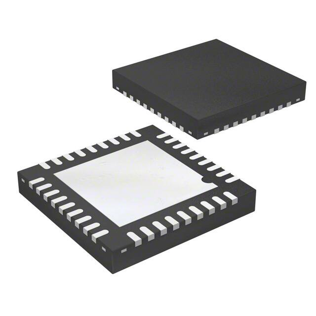
ZL2101
(36 LD QFN)
TOP VIEW
FIGURE 4.
Pin Descriptions
PIN
LABEL
TYPE
(Note 1)
1
PG
O
2
DGND
PWR
3
SYNC
I/O, M
(Note 2)
4
VSET
I, M
Output voltage select pin. Used to set VOUT set-point and VOUT max.
5
SA
I, M
Serial address select pin. Used to assign unique SMBus address to each IC.
6
SCL
I/O
Serial clock. Connect to external host interface.
7
SDA
I/O
Serial data. Connect to external host interface.
8
SALRT
O
9
FC
I, M
Auto compensation configuration pin. Used to set up auto compensation.
10
CFG
I, M
Configuration pin. Used to control the SYNC pin, sequencing and enable tracking.
11
SS
I, M
Soft-start pin. Used to set the ramp delay and ramp time, sets UVLO and configure tracking.
12
VTRK
I
Track sense pin. Used to track an external voltage source.
13
VSEN
I
Output voltage positive feedback sensing pin.
14
SGND
PWR
Common return for analog signals. Connect to low impedance ground plane.
15, 16, 17,
18, 19
PGND
PWR
Power ground. Common return for internal switching MOSFETs. Connect to low impedance ground plane.
20, 21, 22,
23, 24, 25
SW
I/O
26
BST
PWR
Bootstrap voltage for level-shift driver (referenced to SW).
27, 28, 29
VDDP
PWR
Bias supply voltage for internal switching MOSFETs (return is PGND).
30
VDDS
PWR
IC supply voltage (return is SGND).
FN7730 Rev 0.00
January 23, 2012
DESCRIPTION
Power-good. This pin transitions high 100ms after output voltage stabilizes within regulation band.
Selectable open drain or push-pull output. Factory default is open drain.
Digital ground. Common return for digital signals. Connect to low impedance ground plane.
Clock synchronization pin. Used to set switching frequency of internal clock or for synchronization to
external frequency reference.
Serial alert. Connect to external host interface if desired.
Switching node (level-shift common).
Page 3 of 27
�ZL2101
Pin Descriptions (Continued)
PIN
LABEL
TYPE
(Note 1)
31
VR
PWR
Regulated bias from internal 7V low-dropout regulator (return is PGND). Decouple with a 4.7µF capacitor to
PGND.
32
VRA
PWR
Regulated bias from internal 5V low-dropout regulator for internal analog circuitry (return is SGND).
Decouple with a 4.7µF capacitor to SGND.
33
V2P5
PWR
Regulated bias from internal 2.5V low-dropout regulator for internal digital circuitry (return is DGND).
Decouple with a 10µF capacitor.
34
DDC
I/O
35
MGN
I
Margin pin. Used to enable margining of the output voltage.
36
EN
I
Enable pin. Used to enable the device (active high).
ePad
SGND
PWR
DESCRIPTION
Digital-DC Bus (open drain). Interoperability between Zilker Labs devices.
Exposed thermal pad. Common return for analog signals. Connect to low impedance ground plane.
NOTES:
1. I = Input, O = Output, PWR = Power or Ground, M = Multi-mode pins. Please refer to Section “Multi-mode Pins” on page 11.
2. The SYNC pin can be used as a logic pin, a clock input or a clock output.
Ordering Information
PART NUMBER
(Notes 4, 5)
PART MARKING
TEMP RANGE
(°C)
PACKAGE
PKG.
DWG. #
ZL2101ALAF
2101
-40 to +85
36 Ld 6mmx6mm QFN
L36.6x6C
ZL2101ALAFT (Note 3)
2101
-40 to +85
36 Ld 6mmx6mm QFN
L36.6x6C
ZL2101ALAFTK (Note 3)
2101
-40 to +85
36 Ld 6mmx6mm QFN
L36.6x6C
ZL2101EVAL1Z
Evaluation Board
NOTES:
3. Add “-T*” suffix for tape and reel. Please refer to TB347 for details on reel specifications.
4. These Intersil Pb-free plastic packaged products employ special Pb-free material sets, molding compounds/die attach materials, and 100% matte tin
plate plus anneal (e3 termination finish, which is RoHS compliant and compatible with both SnPb and Pb-free soldering operations). Intersil Pb-free
products are MSL classified at Pb-free peak reflow temperatures that meet or exceed the Pb-free requirements of IPC/JEDEC J STD-020.
5. For Moisture Sensitivity Level (MSL), please see device information page for ZL2101. For more information on MSL please see techbrief TB363.
FN7730 Rev 0.00
January 23, 2012
Page 4 of 27
�ZL2101
Table of Contents
Absolute Maximum Ratings. . . . . . . . . . . . . . . . . . . . . . . . . . . . . . . . . . . . . . . . . . . . . . . . . . . . . . . . . . . . . . . . . . . . . . . . . . . . . . . . . . . . . . . . . . . 6
Electrical Specifications . . . . . . . . . . . . . . . . . . . . . . . . . . . . . . . . . . . . . . . . . . . . . . . . . . . . . . . . . . . . . . . . . . . . . . . . . . . . . . . . . . . . . . . . . . . . . . 6
Typical Performance Curves. . . . . . . . . . . . . . . . . . . . . . . . . . . . . . . . . . . . . . . . . . . . . . . . . . . . . . . . . . . . . . . . . . . . . . . . . . . . . . . . . . . . . . . . . . . 9
ZL2101 Overview. . . . . . . . . . . . . . . . . . . . . . . . . . . . . . . . . . . . . . . . . . . . . . . . . . . . . . . . . . . . . . . . . . . . . . . . . . . . . . . . . . . . . . . . . . . . . . . . . . . 10
Digital-DC Architecture . . . . . . . . . . . . . . . . . . . . . . . . . . . . . . . . . . . . . . . . . . . . . . . . . . . . . . . . . . . . . . . . . . . . . . . . . . . . . . . . . . . . . . . . . . . 10
Power Conversion Overview . . . . . . . . . . . . . . . . . . . . . . . . . . . . . . . . . . . . . . . . . . . . . . . . . . . . . . . . . . . . . . . . . . . . . . . . . . . . . . . . . . . . . . . 10
Power Management Overview . . . . . . . . . . . . . . . . . . . . . . . . . . . . . . . . . . . . . . . . . . . . . . . . . . . . . . . . . . . . . . . . . . . . . . . . . . . . . . . . . . . . . 11
Multi-mode Pins . . . . . . . . . . . . . . . . . . . . . . . . . . . . . . . . . . . . . . . . . . . . . . . . . . . . . . . . . . . . . . . . . . . . . . . . . . . . . . . . . . . . . . . . . . . . . . . . . 11
Pin-strap Settings . . . . . . . . . . . . . . . . . . . . . . . . . . . . . . . . . . . . . . . . . . . . . . . . . . . . . . . . . . . . . . . . . . . . . . . . . . . . . . . . . . . . . . . . . . . . 11
Resistor Settings . . . . . . . . . . . . . . . . . . . . . . . . . . . . . . . . . . . . . . . . . . . . . . . . . . . . . . . . . . . . . . . . . . . . . . . . . . . . . . . . . . . . . . . . . . . . . 12
I2C/SMBus Method . . . . . . . . . . . . . . . . . . . . . . . . . . . . . . . . . . . . . . . . . . . . . . . . . . . . . . . . . . . . . . . . . . . . . . . . . . . . . . . . . . . . . . . . . . . 12
Power Conversion Functional Description . . . . . . . . . . . . . . . . . . . . . . . . . . . . . . . . . . . . . . . . . . . . . . . . . . . . . . . . . . . . . . . . . . . . . . . . . . . . . . 12
Internal Bias Regulators and Input Supply Connections . . . . . . . . . . . . . . . . . . . . . . . . . . . . . . . . . . . . . . . . . . . . . . . . . . . . . . . . . . . . . . . 12
High-side Driver Boost Circuit. . . . . . . . . . . . . . . . . . . . . . . . . . . . . . . . . . . . . . . . . . . . . . . . . . . . . . . . . . . . . . . . . . . . . . . . . . . . . . . . . . . . . . 12
Output Voltage Selection . . . . . . . . . . . . . . . . . . . . . . . . . . . . . . . . . . . . . . . . . . . . . . . . . . . . . . . . . . . . . . . . . . . . . . . . . . . . . . . . . . . . . . . . . 12
Start-up Procedure. . . . . . . . . . . . . . . . . . . . . . . . . . . . . . . . . . . . . . . . . . . . . . . . . . . . . . . . . . . . . . . . . . . . . . . . . . . . . . . . . . . . . . . . . . . . . . . 13
Soft-start Delay and Ramp Times . . . . . . . . . . . . . . . . . . . . . . . . . . . . . . . . . . . . . . . . . . . . . . . . . . . . . . . . . . . . . . . . . . . . . . . . . . . . . . . . . . 13
Power-good (PG) . . . . . . . . . . . . . . . . . . . . . . . . . . . . . . . . . . . . . . . . . . . . . . . . . . . . . . . . . . . . . . . . . . . . . . . . . . . . . . . . . . . . . . . . . . . . . . . . 14
Switching Frequency and PLL . . . . . . . . . . . . . . . . . . . . . . . . . . . . . . . . . . . . . . . . . . . . . . . . . . . . . . . . . . . . . . . . . . . . . . . . . . . . . . . . . . . . . 15
Configuration A: SYNC OUTPUT . . . . . . . . . . . . . . . . . . . . . . . . . . . . . . . . . . . . . . . . . . . . . . . . . . . . . . . . . . . . . . . . . . . . . . . . . . . . . . . . . 15
Configuration B: SYNC INPUT . . . . . . . . . . . . . . . . . . . . . . . . . . . . . . . . . . . . . . . . . . . . . . . . . . . . . . . . . . . . . . . . . . . . . . . . . . . . . . . . . . . 15
Configuration C: SYNC AUTO DETECT . . . . . . . . . . . . . . . . . . . . . . . . . . . . . . . . . . . . . . . . . . . . . . . . . . . . . . . . . . . . . . . . . . . . . . . . . . . . 15
Component Selection . . . . . . . . . . . . . . . . . . . . . . . . . . . . . . . . . . . . . . . . . . . . . . . . . . . . . . . . . . . . . . . . . . . . . . . . . . . . . . . . . . . . . . . . . . . . 16
Design Goal Trade-offs . . . . . . . . . . . . . . . . . . . . . . . . . . . . . . . . . . . . . . . . . . . . . . . . . . . . . . . . . . . . . . . . . . . . . . . . . . . . . . . . . . . . . . . . 16
Inductor Selection . . . . . . . . . . . . . . . . . . . . . . . . . . . . . . . . . . . . . . . . . . . . . . . . . . . . . . . . . . . . . . . . . . . . . . . . . . . . . . . . . . . . . . . . . . . . 16
Output Capacitor Selection . . . . . . . . . . . . . . . . . . . . . . . . . . . . . . . . . . . . . . . . . . . . . . . . . . . . . . . . . . . . . . . . . . . . . . . . . . . . . . . . . . . . 17
Input Capacitor . . . . . . . . . . . . . . . . . . . . . . . . . . . . . . . . . . . . . . . . . . . . . . . . . . . . . . . . . . . . . . . . . . . . . . . . . . . . . . . . . . . . . . . . . . . . . . 17
Bootstrap Capacitor Selection . . . . . . . . . . . . . . . . . . . . . . . . . . . . . . . . . . . . . . . . . . . . . . . . . . . . . . . . . . . . . . . . . . . . . . . . . . . . . . . . . . 17
CV2P5 Selection . . . . . . . . . . . . . . . . . . . . . . . . . . . . . . . . . . . . . . . . . . . . . . . . . . . . . . . . . . . . . . . . . . . . . . . . . . . . . . . . . . . . . . . . . . . . . 17
CVR Selection . . . . . . . . . . . . . . . . . . . . . . . . . . . . . . . . . . . . . . . . . . . . . . . . . . . . . . . . . . . . . . . . . . . . . . . . . . . . . . . . . . . . . . . . . . . . . . . 17
CVRA Selection . . . . . . . . . . . . . . . . . . . . . . . . . . . . . . . . . . . . . . . . . . . . . . . . . . . . . . . . . . . . . . . . . . . . . . . . . . . . . . . . . . . . . . . . . . . . . . 18
Thermal Considerations . . . . . . . . . . . . . . . . . . . . . . . . . . . . . . . . . . . . . . . . . . . . . . . . . . . . . . . . . . . . . . . . . . . . . . . . . . . . . . . . . . . . . . . 18
Current Sensing and Current Limit Threshold Selection. . . . . . . . . . . . . . . . . . . . . . . . . . . . . . . . . . . . . . . . . . . . . . . . . . . . . . . . . . . . . . . . 18
Loop Compensation . . . . . . . . . . . . . . . . . . . . . . . . . . . . . . . . . . . . . . . . . . . . . . . . . . . . . . . . . . . . . . . . . . . . . . . . . . . . . . . . . . . . . . . . . . . . . 18
Driver Dead-time Control . . . . . . . . . . . . . . . . . . . . . . . . . . . . . . . . . . . . . . . . . . . . . . . . . . . . . . . . . . . . . . . . . . . . . . . . . . . . . . . . . . . . . . . . . 19
Power Management Functional Description . . . . . . . . . . . . . . . . . . . . . . . . . . . . . . . . . . . . . . . . . . . . . . . . . . . . . . . . . . . . . . . . . . . . . . . . . . . . 19
Input Undervoltage Lockout . . . . . . . . . . . . . . . . . . . . . . . . . . . . . . . . . . . . . . . . . . . . . . . . . . . . . . . . . . . . . . . . . . . . . . . . . . . . . . . . . . . . . . . 19
Output Overvoltage Protection. . . . . . . . . . . . . . . . . . . . . . . . . . . . . . . . . . . . . . . . . . . . . . . . . . . . . . . . . . . . . . . . . . . . . . . . . . . . . . . . . . . . . 19
Output Pre-Bias Protection . . . . . . . . . . . . . . . . . . . . . . . . . . . . . . . . . . . . . . . . . . . . . . . . . . . . . . . . . . . . . . . . . . . . . . . . . . . . . . . . . . . . . . . . 19
Output Overcurrent Protection . . . . . . . . . . . . . . . . . . . . . . . . . . . . . . . . . . . . . . . . . . . . . . . . . . . . . . . . . . . . . . . . . . . . . . . . . . . . . . . . . . . . . 20
Thermal Overload Protection . . . . . . . . . . . . . . . . . . . . . . . . . . . . . . . . . . . . . . . . . . . . . . . . . . . . . . . . . . . . . . . . . . . . . . . . . . . . . . . . . . . . . . 20
Voltage Tracking . . . . . . . . . . . . . . . . . . . . . . . . . . . . . . . . . . . . . . . . . . . . . . . . . . . . . . . . . . . . . . . . . . . . . . . . . . . . . . . . . . . . . . . . . . . . . . . . 21
Tracking Overview . . . . . . . . . . . . . . . . . . . . . . . . . . . . . . . . . . . . . . . . . . . . . . . . . . . . . . . . . . . . . . . . . . . . . . . . . . . . . . . . . . . . . . . . . . . . . . . 21
Tracking Groups . . . . . . . . . . . . . . . . . . . . . . . . . . . . . . . . . . . . . . . . . . . . . . . . . . . . . . . . . . . . . . . . . . . . . . . . . . . . . . . . . . . . . . . . . . . . . . . . . 21
Tracking Configured by Pin-Strap . . . . . . . . . . . . . . . . . . . . . . . . . . . . . . . . . . . . . . . . . . . . . . . . . . . . . . . . . . . . . . . . . . . . . . . . . . . . . . . . . . 22
Voltage Margining . . . . . . . . . . . . . . . . . . . . . . . . . . . . . . . . . . . . . . . . . . . . . . . . . . . . . . . . . . . . . . . . . . . . . . . . . . . . . . . . . . . . . . . . . . . . . . . 22
I2C/SMBus Communications. . . . . . . . . . . . . . . . . . . . . . . . . . . . . . . . . . . . . . . . . . . . . . . . . . . . . . . . . . . . . . . . . . . . . . . . . . . . . . . . . . . . . . 23
I2C/SMBus Device Address Selection. . . . . . . . . . . . . . . . . . . . . . . . . . . . . . . . . . . . . . . . . . . . . . . . . . . . . . . . . . . . . . . . . . . . . . . . . . . . . . . 23
Digital-DC Bus . . . . . . . . . . . . . . . . . . . . . . . . . . . . . . . . . . . . . . . . . . . . . . . . . . . . . . . . . . . . . . . . . . . . . . . . . . . . . . . . . . . . . . . . . . . . . . . . . . 23
Phase Spreading . . . . . . . . . . . . . . . . . . . . . . . . . . . . . . . . . . . . . . . . . . . . . . . . . . . . . . . . . . . . . . . . . . . . . . . . . . . . . . . . . . . . . . . . . . . . . . . . 24
Output Sequencing . . . . . . . . . . . . . . . . . . . . . . . . . . . . . . . . . . . . . . . . . . . . . . . . . . . . . . . . . . . . . . . . . . . . . . . . . . . . . . . . . . . . . . . . . . . . . . 24
Fault Spreading . . . . . . . . . . . . . . . . . . . . . . . . . . . . . . . . . . . . . . . . . . . . . . . . . . . . . . . . . . . . . . . . . . . . . . . . . . . . . . . . . . . . . . . . . . . . . . . . . 25
Monitoring via I2C/SMBus . . . . . . . . . . . . . . . . . . . . . . . . . . . . . . . . . . . . . . . . . . . . . . . . . . . . . . . . . . . . . . . . . . . . . . . . . . . . . . . . . . . . . . . . 25
Snapshot™ Parametric Capture . . . . . . . . . . . . . . . . . . . . . . . . . . . . . . . . . . . . . . . . . . . . . . . . . . . . . . . . . . . . . . . . . . . . . . . . . . . . . . . . . . . 25
Non-Volatile Memory and Device Security Features . . . . . . . . . . . . . . . . . . . . . . . . . . . . . . . . . . . . . . . . . . . . . . . . . . . . . . . . . . . . . . . . . . . 26
Revision History . . . . . . . . . . . . . . . . . . . . . . . . . . . . . . . . . . . . . . . . . . . . . . . . . . . . . . . . . . . . . . . . . . . . . . . . . . . . . . . . . . . . . . . . . . . . . . . . . . . . 26
Products . . . . . . . . . . . . . . . . . . . . . . . . . . . . . . . . . . . . . . . . . . . . . . . . . . . . . . . . . . . . . . . . . . . . . . . . . . . . . . . . . . . . . . . . . . . . . . . . . . . . . . . . . . 26
Package Outline Drawing . . . . . . . . . . . . . . . . . . . . . . . . . . . . . . . . . . . . . . . . . . . . . . . . . . . . . . . . . . . . . . . . . . . . . . . . . . . . . . . . . . . . . . . . . . . . 27
FN7730 Rev 0.00
January 23, 2012
Page 5 of 27
�ZL2101
Absolute Maximum Ratings
Thermal Information
DC Supply Voltage for VDDP, VDDS Pins . . . . . . . . . . . . . . . . . . -0.3V to 17V
High-Side Supply Voltage for BST Pin. . . . . . . . . . . . . . . . . . . . . -0.3V to 25V
High-Side Boost Voltage for BST - SW Pins . . . . . . . . . . . . . . . . . -0.3V to 8V
Internal MOSFET Reference for VR Pin . . . . . . . . . . . . . . . . . . -0.3V to 8.5V
Internal Analog Reference for VRA Pin . . . . . . . . . . . . . . . . . . -0.3V to 6.5V
Internal 2.5V Reference for V2P5 Pin . . . . . . . . . . . . . . . . . . . . . -0.3V to 3V
Logic I/O Voltage for EN, CFG, DDC, FC, MGN, PG, SDA, SCL,
SA, SALRT, SS, SYNC, VTRK, VSET, VSEN Pins . . . . . . . . . . -0.3V to 6.5V
Ground Differential for DGND - SGND,
PGND - SGND Pins . . . . . . . . . . . . . . . . . . . . . . . . . . . . . . . . . . . . . ±0.3V
MOSFET Drive Reference Current for VR Pin
Internal Bias Usage . . . . . . . . . . . . . . . . . . . . . . . . . . . . . . . . . . . . . . 20mA
Switch Node Current for SW Pin
Peak (Sink Or Source) . . . . . . . . . . . . . . . . . . . . . . . . . . . . . . . . . . . . . . 10A
ESD Rating
Human Body Model (Tested per JESD22-A114F) . . . . . . . . . . . . . . . . 2kV
Charged Device Model (Tested per JESD22-C101D) . . . . . . . . . . . . 750V
Machine Model (Tested per JESD22-A115-A) . . . . . . . . . . . . . . . . . 200V
Latch-Up (Tested per JESD78C)
Thermal Resistance (Typical)
JA (°C/W) JC (°C/W)
36 Ld QFN (Notes 6, 7) . . . . . . . . . . . . . . . .
28
1.7
Junction Temperature Range . . . . . . . . . . . . . . . . . . . . . . .-55°C to +150°C
Storage Temperature Range. . . . . . . . . . . . . . . . . . . . . . . .-55°C to +150°C
Dissipation Limits (Note 8)
TA = +25°C . . . . . . . . . . . . . . . . . . . . . . . . . . . . . . . . . . . . . . . . . . . . . . 3.5W
TA = +55°C . . . . . . . . . . . . . . . . . . . . . . . . . . . . . . . . . . . . . . . . . . . . . . 2.5W
TA = +85°C . . . . . . . . . . . . . . . . . . . . . . . . . . . . . . . . . . . . . . . . . . . . . . 1.4W
Pb-Free Reflow Profile . . . . . . . . . . . . . . . . . . . . . . . . . . . . . . . see link below
http://www.intersil.com/pbfree/Pb-FreeReflow.asp
Recommended Operating Conditions
Input Supply Voltage Range, VDDP, VDDS (See Figure 14)
VDDS tied to VR, VRA . . . . . . . . . . . . . . . . . . . . . . . . . . . . . . . . 4.5V to 5.5V
VDDS tied to VR, VRA Floating . . . . . . . . . . . . . . . . . . . . . . . . 5.5V to 7.5V
VR, VRA Floating. . . . . . . . . . . . . . . . . . . . . . . . . . . . . . . . . . . . .7.5V to 14V
Output Voltage Range, VOUT (Note 9) . . . . . . . . . . . . . . . . . . . . 0.54V to 5.5V
Operating Junction Temperature Range, TJ . . . . . . . . . . . . .-40°C to +125°C
CAUTION: Do not operate at or near the maximum ratings listed for extended periods of time. Exposure to such conditions may adversely impact product
reliability and result in failures not covered by warranty.
NOTES:
6. JA is measured in free air with the component mounted on a high effective thermal conductivity test board with “direct attach” features. See Tech
Brief TB379.
7. For JC, the “case temp” location is the center of the exposed metal pad on the package underside.
8. Thermal impedance depends on layout.
9. Includes margin limits.
Electrical Specifications
VDDP = VDDS = 12V, TA = -40°C to +85°C unless otherwise noted. (Note 10) Typical values are at TA = +25°C.
Boldface limits apply over the operating temperature range, -40°C to +85°C.
MIN
(Note 20)
TYP
MAX
(Note 20)
UNIT
fSW = 200kHz, no load
-
11
20
mA
fSW = 1MHz, no load
-
15
30
mA
IDDS Shutdown Current
EN = 0V, No I2C/SMBus activity
-
0.6
1
mA
VR Reference Output Voltage
VDD > 8V, IVR < 10mA
6.5
7.0
7.5
V
VRA Reference Output Voltage
VDD > 5.5V, IVRA < 20mA
4.5
5.1
5.5
V
V2P5 Reference Output Voltage
IV2P5 < 20mA
2.25
2.5
2.75
V
PARAMETER
CONDITIONS
INPUT AND SUPPLY CHARACTERISTICS
IDD Supply Current
OUTPUT CHARACTERISTICS
Output Current
IRMS, Continuous
Output Voltage Adjustment Range (Note 11)
VIN > VOUT
-
-
6
A
0.6
-
5.0
V
Output Voltage Setpoint Resolution
Set using resistors
-
10
-
mV
Set using I2C/SMBus
-
±0.025
-
% FS
(Note 12)
VSEN Output Voltage Accuracy
Includes line, load, temp
-1
-
1
%
VSEN Input Bias Current
VSEN = 5.5V
-
110
200
µA
Soft-start Delay Duration Range (Note 13)
Set using SS pin or resistor
2
-
20
ms
0.002
-
500
s
Set using
FN7730 Rev 0.00
January 23, 2012
I2C/SMBus
Page 6 of 27
�ZL2101
Electrical Specifications
VDDP = VDDS = 12V, TA = -40°C to +85°C unless otherwise noted. (Note 10) Typical values are at TA = +25°C.
Boldface limits apply over the operating temperature range, -40°C to +85°C. (Continued)
MIN
(Note 20)
TYP
MAX
(Note 20)
UNIT
Turn-on delay (precise mode)
(Notes 13, 14)
-
±0.25
-
ms
Turn-on delay (normal mode) (Note 15)
-
-0.25/+4
-
ms
Turn-off delay (Note 15)
-
-0.25/+4
-
ms
Set using SS pin or resistor
2
-
20
ms
0
-
200
ms
-
100
–
µs
-250
-
250
nA
-
-
0.8
V
-
1.4
-
V
2.0
-
-
V
PARAMETER
Soft-start Delay Duration Accuracy
Soft-start Ramp Duration Range
CONDITIONS
Set using
I2C/SMBus
Soft-start Ramp Duration Accuracy
LOGIC INPUT/OUTPUT CHARACTERISTICS
Logic Input Leakage Current
Digital pins
Logic input low, VIL
Logic input OPEN (N/C)
Multi-mode logic pins
Logic Input High, VIH
Logic Output Low, VOL
IOL 4mA
-
-
0.4
V
Logic Output High, VOH
IOH -2mA
2.25
-
-
V
-
-
9
A
200
-
1000
kHz
OSCILLATOR AND SWITCHING CHARACTERISTICS
Switch Node Current, ISW
Peak (source or sink) (Note 16)
Switching Frequency Range
Switching Frequency Set-point Accuracy
Predefined settings (Table 9)
-5
-
5
%
PWM Duty Cycle (max)
Factory default (Note 17)
-
-
95
(Note 18)
%
150
-
-
ns
SYNC Pulse Width (min)
Input Clock Frequency Drift Tolerance
External clock source
-13
-
13
%
rDS(ON) of High Side N-channel FETs
ISW = 6A, VGS = 6.5V
-
60
85
m
rDS(ON) of Low Side N-channel FETs
ISW = 6A, VGS = 12V
-
43
65
m
VTRK Input Bias Current
VTRK = 5.5V
-
110
200
µA
VTRK Tracking Ramp Accuracy
100% Tracking, VOUT - VTRK
-100
-
100
mV
VTRK Regulation Accuracy
100% Tracking, VOUT - VTRK
-1
-
1
%
Configurable via I2C/SMBus
2.85
-
16
V
-150
-
150
mV
-
3
-
%
0
-
100
%
-
-
2.5
µs
TRACKING
FAULT PROTECTION CHARACTERISTICS
UVLO Threshold Range
UVLO Set-point Accuracy
UVLO Hysteresis
Factory default
Configurable via
I2C/SMBus
UVLO Delay
Power-good VOUT Threshold
Factory default
-
90
-
% VOUT
Power-good VOUT Hysteresis
Factory default
-
5
-
%
Power-good Delay
Using pin-strap or resistor
2
-
20
ms
0
-
500
s
Configurable via
FN7730 Rev 0.00
January 23, 2012
I2C/SMBus
Page 7 of 27
�ZL2101
Electrical Specifications
VDDP = VDDS = 12V, TA = -40°C to +85°C unless otherwise noted. (Note 10) Typical values are at TA = +25°C.
Boldface limits apply over the operating temperature range, -40°C to +85°C. (Continued)
PARAMETER
VSEN Undervoltage Threshold
VSEN Overvoltage Threshold
MIN
(Note 20)
TYP
MAX
(Note 20)
UNIT
Factory default
-
85
-
% VOUT
Configurable via I2C/SMBus
0
-
110
% VOUT
Factory default
-
115
-
% VOUT
Configurable via I2C/SMBus
0
-
115
% VOUT
-
5
-
% VOUT
CONDITIONS
VSEN Undervoltage Hysteresis
VSEN Undervoltage/Overvoltage Fault Response
Time
Factory default
-
16
-
µs
Configurable via I2C/SMBus
5
-
60
µs
Peak Current Limit Threshold
Factory default
-
-
9.0
A
0.2
-
9.0
A
-
±10
-
% FS
(Note 12)
Factory default
-
5
-
tSW
(Note 19)
Configurable via I2C/SMBus
1
-
32
tSW
(Note 19)
-
125
-
°C
-40
-
125
°C
-
15
-
°C
Configurable via I2C/SMBus
Current Limit Set-point Accuracy
Current Limit Protection Delay
Thermal Protection Threshold (Junction Temperature) Factory default
Configurable via
I2C/SMBus
Thermal Protection Hysteresis
NOTES:
10. Refer to Safe Operating Area in Figure 8 and thermal design guidelines in AN2010.
11. Does not include margin limits.
12. Percentage of Full Scale (FS) with temperature compensation applied.
13. The device requires a delay period following an enable signal and prior to ramping its output. Precise timing mode limits this delay period to
approximately 2ms, where in normal mode it may vary up to 4ms.
14. Precise ramp timing mode is only valid when using EN pin to enable the device rather than PMBus enable. Precise ramp timing mode is automatically
disabled for a self-enabled device (EN pin tied high).
15. The devices may require up to a 4ms delay following the assertion of the enable signal (normal mode) or following the
de-assertion of the enable signal. Precise mode requires Re-Enable delay = TOFF+TFALL+10µs.
16. Switch node current should not exceed IRMS of 6A.
17. Factory default is the initial value in firmware. The value can be changed via PMBus commands.
18. Maximum duty cycle is limited by the equation MAX_DUTY(%) = [1 - (150×10-9 × fSW)] × 100 and not to exceed 95%.
19. tSW = 1/fSW, where fSW is the switching frequency.
20. Compliance to datasheet limits is assured by one or more methods: production test, characterization and/or design.
FN7730 Rev 0.00
January 23, 2012
Page 8 of 27
�ZL2101
Typical Performance Curves
1.4
1.4
1.3
1.3
NORMALIZED rDS(ON)
NORMALIZED rDS(ON)
For some applications, ZL2101 operating conditions (input voltage, output voltage, switching frequency, temperature) may require de-rating to remain
within the Safe Operating Area (SOA). VIN = VDDP = VDDS, TJ = +125°C
1.2
1.1
1.0
0.9
0.8
0
25
50
75
1.2
1.1
1.0
0.9
0.8
100
0
25
50
TJ (°C)
TJ (°C)
70
6
65
5
60
TJ = +110°C
TJ = +80°C
50
7
8
3
VIN = 8.6V TO 14V
1
TJ = +25°C
6
VIN = 6V
2
TJ = +50°C
40
VIN = 7.5V
4
55
45
100
FIGURE 6. HIGH-SIDE rDS(ON) vs TJ NORMALIZED FOR TJ = +25°C
(VDDS = 12V, BST – SW = 6.5V, IDRAIN = 0.3A)
VOUT (V)
rDS(ON) (m)
FIGURE 5. LOW-SIDE rDS(ON) vs TJ NORMALIZED FOR TJ = +25°C
(VDDS = 12V, IDRAIN = 0.3A)
75
9
10
11
12
0
13
0.2
0.3
0.4
VDDS (V)
0.5
0.6
0.7
0.8
0.9
1
1.0
fSW (MHz)
FIGURE 8. SAFE OPERATING AREA, TJ +125°C
FIGURE 7. LOW-SIDE r DS(ON) vs V DDS WITH TJ
0.95
VOUT MAY NOT EXCEED
5.5V AT ANY TIME
0.90
VOUT/VIN (V)
0.85
0.80
0.75
0.70
0.65
0.60
0.2
0.3
0.4
0.5
0.6
0.7
0.8
0.9
1.0
fSW (MHz)
FIGURE 9. MAXIMUM CONVERSION RATIO, TJ +125°C
FN7730 Rev 0.00
January 23, 2012
Page 9 of 27
�ZL2101
ZL2101 Overview
Digital-DC Architecture
The ZL2101 is an innovative mixed-signal power conversion and
power management IC based on Zilker Labs patented Digital-DC
technology that provides an integrated, high performance stepdown converter for point of load applications. The ZL2101
integrates all necessary PWM control circuitry as well as low
rDS(ON) synchronous power MOSFETs to provide an extremely
small solution for supplying load currents up to 6A.
Its unique PWM loop utilizes an ideal mix of analog and digital
blocks to enable precise control of the entire power conversion
process with no software required, resulting in a very flexible
device that is also very easy to use. An extensive set of power
management functions are fully integrated and can be
configured using simple pin connections. The user configuration
can be saved in an internal non-volatile memory (NVM).
Additionally, all functions can be configured and monitored via
the SMBus hardware interface using standard PMBus
commands, allowing ultimate flexibility.
The ZL2101 can be configured by simply connecting its pins
according to the tables provided in the following sections.
Additionally, a comprehensive set of application notes are
available to help simplify the design process. An evaluation
board is also available to help the user become familiar with the
device. This board can be evaluated as a standalone platform
using pin configuration settings. A Windows™-based GUI is also
provided to enable full configuration and monitoring capability
via the I2C/SMBus interface using an available computer and the
included USB cable.
Power Conversion Overview
The ZL2101 operates as a voltage-mode, synchronous buck
converter with a selectable constant frequency pulse width
modulator (PWM) control scheme. The ZL2101 integrates dual low
rDS(ON) synchronous MOSFETs to minimize the circuit footprint.
Figure 10 illustrates the basic synchronous buck converter
topology showing the primary power train components. This
converter is also called a step-down converter, as the output
voltage must always be lower than the input voltage.
Once enabled, the ZL2101 is immediately ready to regulate
power and perform power management tasks with no
programming required. Advanced configuration options and realtime configuration changes are available via the I2C/SMBus
interface if desired and continuous monitoring of multiple
operating parameters is possible with minimal interaction from a
host controller. Integrated sub-regulation circuitry enables single
supply operation from any external supply between 4.5V and 14V
with no secondary bias supplies needed. The ZL2101 can also be
configured to operate from a 3.3V or 5V standby supply when the
main power rail is not present, allowing the user to configure
and/or read diagnostic information from the device when the
main power has been interrupted or is disabled.
VIN
CIN
LDO
DB
QH
CB
VOUT
QL
FIGURE 10. SYNCHRONOUS BUCK CONVERTER
VTRK
VSET
POWER MANAGEMENT
DIGITAL
DIGITAL
COMPENSATOR
COMPENSATOR
FC
LDO
NVM
BST
ISENSE
HS FET
DRIVER
D-PWM
SYNC
GEN
SYNC
VDDP
SS
VDDS
EN MGN CFG
>
VRA
VR
PG
COUT
ZL
INPUT VOLTAGE BUS
>
L1
PWM
SW
VOUT
LS FET
DRIVER
PLL
ADC
-
+
ISENSE
ADC
RESET
REF
DDC
SALRT
SDA
SCL
SA
VDD
ADC
COMMUNICATION
VSEN
MUX
TEMP
SENSOR
FIGURE 11. ZL2101 BLOCK DIAGRAM
FN7730 Rev 0.00
January 23, 2012
Page 10 of 27
�ZL2101
The ZL2101 integrates two N-channel power MOSFETs; QH is the
top control MOSFET and QL is the bottom synchronous MOSFET.
The amount of time that QH is on as a fraction of the total
switching period is known as the duty cycle D, which is described
by Equation 1:
D
VOUT
VIN
(EQ. 1)
During time D, QH is on and VIN – VOUT is applied across the
inductor. The output current ramps up as shown in Figure 12.
When QH turns off (time 1-D), the current flowing in the inductor
must continue to flow from the ground up through QL, during which
the current ramps down. Since the output capacitor COUT exhibits
low impedance at the switching frequency, the AC component of the
inductor current is filtered from the output voltage so the load sees
nearly a DC voltage.
The maximum conversion ratio is shown in Figure 9. Typically,
buck converters specify a maximum duty cycle that effectively
limits the maximum output voltage that can be realized for a
given input voltage and switching frequency. This duty cycle limit
ensures that the low-side MOSFET is allowed to turn on for a
minimum amount of time during each switching cycle, which
enables the bootstrap capacitor to be charged up and provide
adequate gate drive voltage for the high-side MOSFET.
VIN - VOUT
IO
0
Current (A)
Voltage
(V)
IL PK
ILV
-VOUT
value with an analog to digital (A/D) converter. The digital signal
is also applied to an adjustable digital compensation filter and
the compensated signal is used to derive the appropriate PWM
duty cycle for driving the internal MOSFETs in a way that
produces the desired output.
Power Management Overview
The ZL2101 incorporates a wide range of configurable power
management features that are simple to implement without
additional components. Also, the ZL2101 includes circuit protection
features that continuously safeguard the device and load from
damage due to unexpected system faults. The ZL2101 can
continuously monitor input voltage, output voltage/current and
internal temperature. A Power-good output signal is also included to
enable power-on reset functionality for an external processor.
All power management functions can be configured using either
pin configuration techniques (see Figure 13) or via the
I2C/SMBus interface. Monitoring parameters can also be preconfigured to provide alerts for specific conditions. See
Application Note AN2033 for more details on SMBus monitoring.
Multi-mode Pins
In order to simplify circuit design, the ZL2101 incorporates
patented multi-mode pins that allow the user to easily configure
many aspects of the device without programming. Most power
management features can be configured using these pins. The
multi-mode pins can respond to four different connections, as
shown in Table 1. These pins are sampled when power is applied
or by issuing a PMBus Restore command (See Application Note
AN2033).
PIN-STRAP SETTINGS
This is the simplest method, as no additional components are
required. Using this method, each pin can take on one of three
possible states: LOW, OPEN, or HIGH. These pins can be
connected to the V2P5 pin for logic HIGH settings as this pin
provides a regulated voltage higher than 2V. Using a single pin
one of three settings can be selected.
TABLE 1. MULTI-MODE PIN CONFIGURATION
D
1-D
PIN TIED TO
VALUE
FIGURE 12. INDUCTOR WAVEFORM
LOW (Logic LOW)
< 0.8VDC
In general, the size of components L1 and COUT as well as the
overall efficiency of the circuit are inversely proportional to the
switching frequency, fSW. Therefore, the highest efficiency circuit
may be realized by switching the MOSFETs at the lowest possible
frequency; however, this will result in the largest component size.
Conversely, the smallest possible footprint may be realized by
switching at the fastest possible frequency but this gives a
somewhat lower efficiency. Each user should determine the
optimal combination of size and efficiency when determining the
switching frequency for each application.
OPEN (N/C)
No connection
HIGH (Logic HIGH)
> 2.0VDC
Resistor to SGND
Set by resistor value
Time
The block diagram for the ZL2101 is illustrated in Figure 11. In
this circuit, the target output voltage is regulated by connecting
the VSEN pin directly to the output regulation point. The VSEN
signal is then compared to an internal reference voltage that had
been set to the desired output voltage level by the user. The error
signal derived from this comparison is converted to a digital
FN7730 Rev 0.00
January 23, 2012
Logic
high
Open
ZL
ZL
Multi- mode Pin
Multi- mode Pin
RSET
Logic
low
Pinstrap
Settings
Resistor
Settings
FIGURE 13. PIN-STRAP AND RESISTOR SETTING EXAMPLES
Page 11 of 27
�ZL2101
RESISTOR SETTINGS
This method allows a greater range of adjustability when
connecting a finite value resistor (in a specified range) between
the multi-mode pin and SGND.
Standard 1% resistor values are used, and only every fourth E96
resistor value is used so the device can reliably recognize the
value of resistance connected to the pin while eliminating the
error associated with the resistor accuracy. Up to 31 unique
selections are available using a single resistor.
I2C/SMBUS METHOD
ZL2101 functions can be configured via the I2C/SMBus interface
using standard PMBus commands. Additionally, any value that
has been configured using the pin-strap or resistor setting
methods can also be re-configured and/or verified via the
I2C/SMBus. See Application Note AN2033 for more details.
The SMBus device address and VOUT_MAX are the only
parameters that must be set by external pins. All other device
parameters can be set via the I2C/SMBus. The device address is
set using the SA pin. VOUT_MAX is determined as 10% greater
than the voltage set by the VSET pin.
Resistor pin-straps are recommended to be used for all available
device parameters to allow a safe initial power-up before
configuration is stored via the I2C/SMBus. For example, this can
be accomplished by pin-strapping the undervoltage lockout
threshold (using SS pin) to a value greater than the expected
input voltage, thus preventing the device from enabling prior to
loading a configuration file.
Power Conversion Functional
Description
Internal Bias Regulators and Input Supply
Connections
The ZL2101 employs three internal low dropout (LDO) regulators
to supply bias voltages for internal circuitry, allowing it to operate
from a single input supply. The internal bias regulators are as
follows:
• VR: The VR LDO provides a regulated 7V bias supply for the
high-side MOSFET driver circuit. It is powered from the VDDS
pin and supplies bias current internally. A 4.7µF filter capacitor
is required at the VR pin. The VDDS pin directly supplies the
low-side MOSFET driver circuit.
• VRA: The VRA LDO provides a regulated 5V bias supply for the
current sense circuit and other analog circuitry. It is powered
from the VDDS pin and supplies bias current internally. A
4.7µF filter capacitor is required at the VRA pin.
FN7730 Rev 0.00
January 23, 2012
VIN
VIN
VIN
VDDS
VDDS
VDDS
VR
VR
VR
VRA
VRA
VRA
4.5V ≤ VIN ≤ 5.5V
5.5V < V IN ≤ 7.5V
7.5V < V IN ≤ 14V
FIGURE 14. INPUT SUPPLY CONNECTIONS
• V2P5:The V2P5 LDO provides a regulated 2.5V bias supply for
the main controller circuitry. It is powered from the VRA LDO
and supplies bias current internally. A 10µF filter capacitor is
required at the V2P5 pin.
When the input supply (VDDS) is higher than 7.5V, the VR and
VRA pins should not be connected to any other pins. These pins
should only have a filter capacitor attached. Due to the dropout
voltage associated with the VR and VRA bias regulators, the
VDDS pin must be connected to these pins for designs operating
from a supply below 7.5V. Figure 14 illustrates the required
connections for all cases.
Note: The internal bias regulators, VR and VRA, are not designed
to be outputs for powering other circuitry. Do not attach external
loads to any of these pins. Only the multi-mode pins may be
connected to the V2P5 pin for logic HIGH settings.
High-side Driver Boost Circuit
The gate drive voltage for the high-side MOSFET driver is
generated by a floating bootstrap capacitor, CB (see Figure 10).
When the lower MOSFET (QL) is turned on, the SW node is pulled
to ground and the capacitor is charged from the internal VR bias
regulator through diode DB. When QL turns off and the upper
MOSFET (QH) turns on, the SW node is pulled up to VDDP and the
voltage on the bootstrap capacitor is boosted approximately 6.5V
above VDDP to provide the necessary voltage to power the highside driver. An internal Schottky diode is used with CB to help
maximize the high-side drive supply voltage.
Output Voltage Selection
The output voltage may be set to any voltage between 0.6V and
5.0V provided that the input voltage is higher than the desired
output voltage by an amount sufficient to prevent the device
from exceeding its maximum duty cycle specification. Using the
pin-strap method, VOUT can be set to one of three standard
voltages as shown in Table 2.
TABLE 2. PIN-STRAP OUTPUT VOLTAGE SETTINGS
VSET
VOUT
LOW
1.2V
OPEN
1.5V
HIGH
3.3V
Page 12 of 27
�ZL2101
TABLE 3. ZL2101 START-UP SEQUENCE
STEP #
STEP NAME
DESCRIPTION
1
Power Applied
2
Internal Memory Check
The device will check for values stored in its internal memory. This
step is also performed after a Restore command.
3
Multi-mode Pin Check
The device loads values configured by the multi-mode pins.
4
Device Ready
5
Pre-ramp Delay
Input voltage is applied to the ZL2101’s VDD pins (VDDP and VDDS). Depends on input supply ramp time
Approximately 5ms to 10ms (device
will ignore an enable signal or
PMBus traffic during this period)
The device is ready to accept an enable signal.
-
The device requires approximately 2ms following an enable signal
and prior to ramping its output. Additional pre-ramp delay may be
configured using the SS pin.
Approximately 2ms
TABLE 4. RESISTORS FOR SETTING OUTPUT VOLTAGE
RSET
(k)
VOUT
(V)
10
0.6
11
0.7
12.1
0.75
13.3
0.8
14.7
0.9
16.2
1.0
17.8
1.1
19.6
1.2
21.5
1.25
23.7
1.3
26.1
1.4
28.7
1.5
31.6
1.6
34.8
1.7
38.3
1.8
42.2
1.9
46.4
2.0
51.1
2.1
56.2
2.2
61.9
2.3
68.1
2.4
75
2.5
82.5
2.6
90.9
2.7
100
2.8
110
2.9
121
3.0
133
3.1
147
3.2
162
3.3
178
5.0
FN7730 Rev 0.00
January 23, 2012
TIME DURATION
The resistor setting method can be used to set the output voltage
to levels not available in Table 2. To set VOUT using resistors, use
Table 4 to select the resistor that corresponds to the desired
voltage.
The output voltage may also be set to any value between 0.6V
and 5.0V using the I2C interface. See Application Note AN2033
for details.
Start-up Procedure
The ZL2101 follows a specific internal start-up procedure after
power is applied to the VDD pins (VDDP and VDDS). Table 3
describes the start-up sequence.
If the device is to be synchronized to an external clock source, the
clock frequency must be stable prior to asserting the EN pin. The
device requires approximately 5ms to 10ms to check for specific
values stored in its internal memory. If the user has stored values
in memory, those values will be loaded. The device will then
check the status of all multi-mode pins and load the values
associated with the pin settings.
Once this process is completed, the device is ready to accept
commands via the I2C/SMBus interface and the device is ready
to be enabled. Once enabled, the device requires approximately
2ms before its output voltage may be allowed to start its
ramp-up process. If a soft-start delay period less than 2ms has
been configured (using PMBus commands), the device will
default to a 2ms delay period. If a delay period greater than 2ms
is configured, the device will wait for the configured delay period
prior to starting to ramp its output.
After the delay period has expired, the output will begin to ramp
towards its target voltage according to the pre-configured
soft-start ramp time that has been set using the SS pin. It should
be noted that if the EN pin is tied to VDDP or VDDS, the device
will still require approximately 5ms to 10ms before the output
can begin its ramp-up as described in Table 3.
Soft-start Delay and Ramp Times
It may be necessary to set a delay from when an enable signal is
received until the output voltage starts to ramp to its target
value. In addition, the designer may wish to set the time required
for VOUT to ramp to its target value after the delay period has
expired. These features may be used as part of an overall inrush
current management strategy or to control how fast a load IC is
turned on. The ZL2101 gives the system designer several options
for precisely and independently controlling both the delay and
ramp time periods.
Page 13 of 27
�ZL2101
The soft-start delay period begins when the EN pin is asserted
and ends when the delay time expires. The soft-start delay period
is set using the SS pin. Precise ramp delay timing mode reduces
the delay time variations and is available when the appropriate
bit in the MISC_CONFIG register had been set. Please refer to
Application Note AN2033 for details.
The soft-start ramp timer enables a precisely controlled ramp to
the nominal VOUT value that begins once the delay period has
expired. The ramp-up is guaranteed monotonic and its slope may
be precisely set using the SS pin. Using the pin-strap method, the
soft-start delay and ramp times can be set to one of three
standard values according to Table 5.
TABLE 5. SOFT-START DELAY AND RAMP SETTINGS
SS PIN SETTING
DELAY AND
RAMP TIME
(ms)
LOW
2
OPEN
5
HIGH
10
UVLO
7.5V
If the desired soft-start delay and ramp times are not one of the
values listed in Table 5, the times can be set to a custom value by
connecting a resistor from the SS pin to SGND using the
appropriate resistor value from Table 6. The value of this resistor
is measured upon start-up or Restore and will not change if the
resistor is varied after power has been applied to the ZL2101
(see Figure 15).
SS
ZL
RSS
FIGURE 15. SS PIN RESISTOR CONNECTIONS
The soft-start delay and ramp times can also be set to custom
values via the I2C/SMBus interface. When the SS delay time is
set to 0ms, the device will begin its ramp-up after the internal
circuitry has initialized (~2ms). When the soft-start ramp period
is set to 0ms, the output will ramp up as quickly as the output
load capacitance and loop settings will allow. It is generally
recommended to set the soft-start ramp to a value greater than
500µs to prevent inadvertent fault conditions due to excessive
inrush current.
TABLE 6. DELAY AND RAMP CONFIGURATION
RSS
(k)
DELAY TIME
(ms)
10
5
11
10
12.1
20
13.3
5
14.7
10
16.2
20
17.8
5
19.6
10
21.5
20
23.7
5
26.1
10
28.7
20
31.6
5
34.8
10
38.3
20
42.2
5
46.4
10
51.1
20
56.2
5
61.9
10
68.1
20
75
5
82.5
10
90.9
20
100
5
110
10
121
20
133
5
147
10
162
20
RAMP TIME
(ms)
UVLO
(V)
5
4.5
10
2
5
5.5
10
20
2
5
7.5
10
20
Note that when Auto Compensation is enabled, the minimum
tON_DELAY is 5ms.
Power-good (PG)
The ZL2101 provides a Power-good (PG) signal that indicates the
output voltage is within a specified tolerance of its target level
and no fault condition exists. By default, the PG pin will assert if
the output is within +15%/-10% of the target voltage. These
limits may be changed via the I2C/SMBus interface. See
Application Note AN2033 for details.
A PG delay period is the time from when all conditions for
asserting PG are met and when the PG pin is actually asserted.
This feature is commonly used instead of an external reset
controller to signal the power supply is at its target voltage prior
to enabling any powered circuitry. By default, the ZL2101 PG
delay is set to 1ms and may be changed using the I2C/SMBus
interface as described in AN2033.
FN7730 Rev 0.00
January 23, 2012
Page 14 of 27
�ZL2101
Switching Frequency and PLL
The ZL2101 incorporates an internal phase-locked loop (PLL) to
clock the internal circuitry. The PLL can be driven by an external
clock source connected to the SYNC pin. When using the internal
oscillator, the SYNC pin can be configured as a clock source for
other Zilker Labs devices.
The SYNC pin is a unique pin that can perform multiple functions
depending on how it is configured. The CFG pin is used to select
the operating mode of the SYNC pin as shown in Table 4.
Figure 16 illustrates the typical connections for each mode.
TABLE 7. SYNC PIN FUNCTION SELECTION
CFG PIN
LOW
SYNC PIN FUNCTION
SYNC is configured as an input
OPEN
Auto detect mode
HIGH
SYNC is configured as an output fSW = 400kHz
CONFIGURATION A: SYNC OUTPUT
When the SYNC pin is configured as an output (CFG pin is tied
HIGH), the device will run from its internal oscillator and will drive
the resulting internal oscillator signal (preset to 400kHz) onto the
SYNC pin so other devices can be synchronized to it. The SYNC
pin will not be checked for an incoming clock signal while in this
mode.
200kHz to 1MHz with a minimum duty cycle and must be stable
when the EN pin is asserted. The external clock signal must also
exhibit the necessary performance requirements (see the
“Electrical Specifications” table beginning on page 6).
In the event of a loss of the external clock signal, the output
voltage may show transient over/undershoot. If this happens, the
ZL2101 will automatically switch to its internal oscillator and
switch at a frequency close to the previous incoming frequency.
CONFIGURATION C: SYNC AUTO DETECT
When the SYNC pin is configured in auto detect mode (CFG pin is
left OPEN), the device will automatically check for a clock signal
on the SYNC pin after enable is asserted. If a valid clock signal is
present, the ZL2101’s oscillator will then synchronize with the
rising edge of the external clock (refer to SYNC INPUT
description).
If no incoming clock signal is present, the ZL2101 will configure
the switching frequency according to the state of the SYNC pin as
listed in Table 8. In this mode, the ZL2101 will only read the
SYNC pin connection during the start-up sequence. Changes to
the SYNC pin connection will not affect fSW until the power
(VDDS) is cycled off and on again.
TABLE 8. SWITCHING FREQUENCY SELECTION
SYNC PIN
FREQUENCY
CONFIGURATION B: SYNC INPUT
LOW
200kHz
When the SYNC pin is configured as an input (CFG pin is tied
LOW), the device will automatically check for an external clock
signal on the SYNC pin each time the EN pin is asserted. The
internal oscillator will then synchronize with the rising edge of the
external clock. The incoming clock signal must be in the range of
OPEN
400kHz
HIGH
1MHz
Resistor
See Table 9
SYNC
200kHz – 1MHz
ZL2101
ZL2106
ZL2106
ZL2101
N/C
Open
SYNC
OR
Logic
low
N/C
CFG
SYNC
200kHz – 1MHz
B) SYNC = input
Logic
high
CFG
N/C
ZL2101
ZL2106
ZL2106
ZL2101
SYNC
OR
RSYNC
CFG
A) SYNC = output
CFG
SYNC
200kHz – 1MHz
CFG
Logic
high
ZL2106
ZL2101
C) SYNC = Auto Detect
FIGURE 16. SYNC PIN CONFIGURATIONS
FN7730 Rev 0.00
January 23, 2012
Page 15 of 27
�ZL2101
If the user wishes to run the ZL2101 at a frequency not listed in
Table 8, the switching frequency can be set using an external
resistor, RSYNC, connected between SYNC and SGND using Table 9.
TABLE 9. RSYNC RESISTOR VALUES
RSYNC
(k)
FSW
(kHz)
10
200
11
222
12.1
242
13.3
267
14.7
296
16.2
320
17.8
364
19.6
400
21.5
421
23.7
471
26.1
533
28.7
571
TABLE 10. POWER SUPPLY REQUIREMENTS
PARAMETER
RANGE
EXAMPLE
VALUE
Input voltage (VIN)
4.5V to
14.0V
12V
Output voltage (VOUT)
0.6V to
5.0V
3.3V
Output current (IOUT)
0A to 6A
4A


 工商网监
湘ICP备2023018690号
工商网监
湘ICP备2023018690号
