R3116x-Y Series
0.8% Low Voltage Detector with Output Delay for Industrial Applications
NO.EA-347-170203
OUTLINE
The R3116x is a CMOS-based voltage detector IC with high detector threshold accuracy and ultra-low supply
current, which can be operated at an extremely low voltage and is used for system reset as an example.
This IC consists of a voltage reference unit, a comparator, resistors for detector threshold setting, an output
driver, a hysteresis circuit and an output delay circuit. The detector threshold is internally fixed with high accuracy
and does not require any adjustment.
Two output types, Nch open drain type and CMOS type are available.
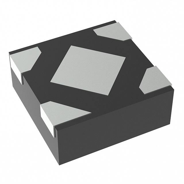
R3116x is offered in a 5-pin SOT-23-5 package and an ultra-small 4-pin DFN(PLP)1010-4 package which can
achieve the smallest possible footprint solution on boards where area is limited.
This is a high-reliability semiconductor device for industrial applications (-Y) that has passed both the screening
at high temperature and the reliability test with extended hours. This line of products operate in a wide temperature
range from low temperature to high temperature to support harsh environment applications.
FEATURES
• Operating Voltage Range (Maximum Rating) ....................... 0.5V to 6.0V (7.0V)
• Operating Temperature Range ............................................. −50°C to 105°C
• Supply Current ...................................................................... Typ. 0.35µA (-VDET=1.5V, VDD=-VDET+1V)
• Detector Threshold Range .................................................... 0.7V to 5.0V (0.1V steps)
• Detector Threshold Accuracy ................................................ ±0.8% (-VDET ≥ 1.5V)
• Temperature-Drift Coefficient of Detector Threshold ............ Typ. ±30ppm/°C
• Built-in Output Delay Circuit .................................................. Typ. 100ms with an external capacitor: 0.022µF
• Output Delay Time Accuracy................................................. ±15% (-VDET ≥ 1.5V)
• Output Types ......................................................................... Nch Open Drain and CMOS
• Packages .............................................................................. DFN(PLP)1010-4, SOT-23-5
APPLICATIONS
• Industrial equipments such as FAs and smart meters
• Equipments used under high-temperature conditions such as surveillance camera and vending machine
• Equipments accompanied by self-heating such as motor and lighting
1
�R3116x-Y
NO.EA-347-170203
BLOCK DIAGRAMS
Nch Open Drain Output (R3116xxx1A)
VDD
CMOS Output (R3116xxx1C)
OUT
VDD
Delay
Circuit
Delay
Circuit
OUT
Vref
Vref
GND
GND
CD
CD
SELECTION GUIDE
The package type, the detector threshold, the output type and the taping type for the ICs can be selected at the
users’ request.
Product Name
R3116Kxx1∗-TR-Y
R3116Nxx1∗-TR-YE
Package
Quantity per Reel
Pb Free
Halogen Free
DFN(PLP)1010-4
10,000 pcs
Yes
Yes
SOT-23-5
3,000 pcs
Yes
Yes
xx : The set detector threshold (-VSET) can be designated in the range from 0.7V(07) to 5.0V(50) in 0.1V
steps.
∗ : Designation of Output Type
(A) Nch Open Drain
(C) CMOS
2
�R3116x-Y
NO.EA-347-170203
PIN DESCRIPTIONS
• DFN(PLP)1010-4
Top View
• SOT-23-5
Bottom View
5
4
3
3
4
4
∗
(mark side)
1
•
2
2
1
1
2
3
DFN(PLP)1010-4
Pin No.
Symbol
1
OUT
2
CD
3
GND
4
VDD
Description
Output Pin ("L" at detection)
Pin for External Capacitor (for setting output delay)
Ground Pin
Input Pin
∗) The tab on the bottom of the package enhances thermal performance and is electrically connected to GND (substrate
level). It is recommended that the tab be connected to the ground plane on the board, or otherwise be left open.
•
SOT-23-5
Pin No.
Symbol
Description
1
OUT
Output Pin ("L" at detection)
2
VDD
Input Pin
3
GND
4
NC
No Connection
5
CD
Pin for External Capacitor (for setting output delay)
Ground Pin
3
�R3116x-Y
NO.EA-347-170203
ABSOLUTE MAXIMUM RATINGS
Symbol
VDD
VOUT
IOUT
PD
Tj
Tstg
Item
Rating
Unit
7.0
V
Supply Voltage
VSS−0.3 to 7.0
Output Voltage (Nch Open Drain Output)
V
VSS−0.3 to VDD+0.3
Output Voltage (CMOS Output)
Output Current
20
Power Dissipation (DFN(PLP)1010-4)*
Standard Land Pattern
400
Power Dissipation (SOT-23-5) *
Standard Land Pattern
420
mA
mW
Junction Temperature
−50 to 125
°C
Storage Temperature Range
−55 to 125
°C
∗ Please refer to PACKAGE INFORMATION for detailed information.
ABSOLUTE MAXIMUM RATINGS
Electronic and mechanical stress momentarily exceeded absolute maximum ratings may cause the
permanent damages and may degrade the life time and safety for both device and system using the device
in the field. The functional operation at or over these absolute maximum ratings are not assured.
RECOMMENDED OPERATING CONDITIONS
Symbol
Item
Rating
Unit
VDD
Operating Voltage
0.60 to 6.0
V
Ta
Operating Temperature Range
−50 to 105
°C
RECOMMENDED OPERATING CONDITIONS
All of electronic equipment should be designed that the mounted semiconductor devices operate within the
recommended operating conditions. The semiconductor devices cannot operate normally over the
recommended operating conditions, even if when they are used over such conditions by momentary
electronic noise or surge. And the semiconductor devices may receive serious damage when they continue
to operate over the recommended operating conditions.
4
�R3116x-Y
NO.EA-347-170203
ELECTRICAL CHARACTERISTICS
are guaranteed by design engineering at -50°C ≤ Ta ≤ 105°C.
The specifications surrounded by
•
R3116xxx1A/C
Symbol
(Ta=25°C)
Item
Conditions
1.5V < −VDET ≤ 5.0V
Ta=25°C
-VDET
Min.
0.7V ≤ −VDET ≤ 1.5V
Detector Threshold
−50°C ≤ Ta ≤ 105°C
1.5V < −VDET ≤ 5.0V
0.7V ≤ −VDET ≤ 1.5V
VHYS
Detector Threshold
Hysteresis
VDD= −VDET −0.1V
ISS
Supply Current
VDD= −VDET +1.0V
VDDL
Minimum Operating
Voltage∗1
−VDET
×1.008
+12
−VDET
×0.985
-22.5
−VDET
×1.015
+22.5
−VDET
× 0.04
−VDET
× 0.07
1.400
1.6V ≤ −VDET < 3.1V
1.500
3.1V ≤ −VDET < 4.1V
1.600
4.1V ≤ −VDET ≤ 5.0V
1.700
0.7V ≤ −VDET < 1.6V
1.200
1.6V ≤ −VDET < 3.1V
1.200
3.1V ≤ −VDET < 4.1V
1.300
4.1V ≤ −VDET ≤ 5.0V
1.400
0.50
−40°C ≤ Ta ≤ 105°C
0.55
−50°C ≤ Ta ≤ 105°C
0.60
Output Current
(Driver Output Pin)
VDD=0.6V
VDS=0.5V
0.020
1.1V ≤ −VDET < 1.6V
VDD=1.0V
VDS=0.5V
0.400
1.6V ≤ −VDET < 3.1V
VDD=1.5V
VDS=0.5V
1.000
3.1V ≤ −VDET ≤ 5.0V
VDD=3.0V
VDS=0.5V
2.400
0.7V ≤ −VDET < 4.0V
VDD=4.5V
VDS=−2.1V
0.650
4.0V ≤ −VDET ≤ 5.0V
VDD=6.0V
VDS=−2.1V
0.900
Pch
Output Delay Time
V
mV
V
mV
V
µA
V
V
mA
mA
Nch Driver Leakage Current∗3 VDD=6.0V, VDS=7.0V
80
0.7V≤ −VDET < 1.5V
80
1.5V≤ −VDET ≤5.0V
CD=0.022µF,
VDD=−VDET−0.1V
−50°C ≤ Ta ≤ 0.7V≤ −VDET < 1.5V
to −VDETx1.1V
105°C
1.5V≤ −VDET ≤5.0V
85
Ta=25°C
Unit
µA
7
0.7V ≤ −VDET < 1.1V
∗2
tD
−VDET
× 0.992
-12
Ta=25°C
Nch
ILEAK
Max.
0.7V ≤ −VDET < 1.6V
VDD=0.55V, VDS=0.05V
IOUT
Typ.
100
70
nA
130
115
150
ms
100
75
135
All of unit are tested and specified under load conditions such that Tj≈Ta=25°C
*1 Minimum operating voltage means the value of input voltage when output voltage maintains 0.1V or less.
(In case of Nch Open Drain Output type, the output pin is pulled up with a resistance of 470kΩ to 5.0V)
*2 In case of CMOS type
*3 In case of Nch Open Drain type
5
�R3116x-Y
NO.EA-347-170203
TIMING CHART
Supply
Voltage
(VDD)
Released Voltage (+VDET)
CD Pin
Voltage
CD Pin Threshold Voltage
(VTCD)
Detector Threshold (-VDET)
GND
Output
Voltage
(VOUT)
GND
Output Delay Time (tD) Detect Delay Time (tPHL)
•
When the supply voltage, which is higher than
released voltage, is forced to VDD pin, charge to
an external capacitor starts, then CD pin voltage
increases. Until the CD pin voltage reaches to CD
pin threshold voltage, output voltage maintains
"L". When the CD pin voltage becomes higher
than CD pin threshold voltage, output voltage is
reversed from "L" to "H". Where the time interval
between the rising edge of supply voltage and
output voltage reverse point means output delay
time.
When the output voltage reverses from "L" to
"H", the external capacitor starts to discharge.
Therefore, when lower voltage than the detector
threshold voltage is forced to VDD pin, the output
voltage reverses from "H" to "L" thus the detect
delay time is constant not being affected by the
external capacitor.
Output Delay Time
Output Delay Time (tD) can be calculated with the next formula using the external capacitor:
tD(s) = 4.5 × 10⁶ × CD(F)
DEFINITION OF OUTPUT DELAY TIME
Output Delay Time (tD) is defined as follows:
1. In the case of Nch Open Drain Output:
Under the condition of the output pin (OUT) is pulled up through a resistor of 470kΩ to 5V, the time interval
between the rising edge of VDD pulse from (-VDET)−0.1V to (-VDET)×1.1V pulse voltage is supplied, the becoming
of the output voltage to 2.5V.
2. In the case of CMOS Output:
The time interval between the rising edge of VDD pulse from (-VDET)−0.1V to (-VDET)×1.1V pulse voltage is
supplied, the becoming of the output voltage to ((-VDET)×1.1V)/2.
−VDET×1.1V
Supply
Voltage
(VDD) −VDET−0.1V
Output
Voltage
(VOUT)
−VDET×1.1V
GND
Supply
Voltage
(VDD) −VDET−0.1V
GND
5.0V
−VDET×1.1V
2.5V
(−VDET×1.1V)/2
Output
Voltage
GND
(VOUT)
GND
tPHL
6
tD
tPHL
Nch Open Drain Output
CMOS Output
(R3116xxx1A)
(R3116xxx1C)
tD
�R3116x-Y
NO.EA-347-170203
ELECTRICAL CHARACTERISTICS BY DETECTOR THRESHOLD
•
R3116x071A/C to R3116x501A/C
Bold values are checked and guaranteed by design engineering at −50°C ≤ Ta ≤ 105°C, unless otherwise noted.
(Ta=25°C)
Part
Number
R3116x071A/C
R3116x081A/C
R3116x091A/C
R3116x101A/C
R3116x111A/C
R3116x121A/C
R3116x131A/C
R3116x141A/C
R3116x151A/C
R3116x161A/C
R3116x171A/C
R3116x181A/C
R3116x191A/C
R3116x201A/C
R3116x211A/C
R3116x221A/C
R3116x231A/C
R3116x241A/C
R3116x251A/C
R3116x261A/C
R3116x271A/C
R3116x281A/C
R3116x291A/C
R3116x301A/C
R3116x311A/C
R3116x321A/C
R3116x331A/C
R3116x341A/C
R3116x351A/C
R3116x361A/C
R3116x371A/C
R3116x381A/C
R3116x391A/C
R3116x401A/C
R3116x411A/C
R3116x421A/C
R3116x431A/C
R3116x441A/C
R3116x451A/C
R3116x461A/C
R3116x471A/C
R3116x481A/C
R3116x491A/C
R3116x501A/C
Detector
Threshold1
-VDET1 [V]
Min.
0.688
0.788
0.888
0.988
1.088
1.188
1.288
1.388
1.488
1.587
1.686
1.786
1.885
1.984
2.083
2.182
2.282
2.381
2.480
2.579
2.678
2.778
2.877
2.976
3.075
3.174
3.274
3.373
3.472
3.571
3.670
3.770
3.869
3.968
4.067
4.166
4.266
4.365
4.464
4.563
4.662
4.762
4.861
4.960
Max.
0.712
0.812
0.912
1.012
1.112
1.212
1.312
1.412
1.512
1.613
1.714
1.814
1.915
2.016
2.117
2.218
2.318
2.419
2.520
2.621
2.722
2.822
2.923
3.024
3.125
3.226
3.326
3.427
3.528
3.629
3.730
3.830
3.931
4.032
4.133
4.234
4.334
4.435
4.536
4.637
4.738
4.838
4.939
5.040
Detector
Threshold2
-VDET2 [V]
Min.
0.678
0.778
0.878
0.978
1.078
1.178
1.278
1.378
1.478
1.576
1.675
1.773
1.872
1.970
2.069
2.167
2.266
2.364
2.463
2.561
2.660
2.758
2.857
2.955
3.054
3.152
3.251
3.349
3.448
3.546
3.645
3.743
3.842
3.940
4.039
4.137
4.236
4.334
4.433
4.531
4.630
4.728
4.827
4.925
Max.
0.723
0.823
0.923
1.023
1.123
1.223
1.323
1.423
1.523
1.624
1.726
1.827
1.929
2.030
2.132
2.233
2.335
2.436
2.538
2.639
2.741
2.842
2.944
3.045
3.147
3.248
3.350
3.451
3.553
3.654
3.756
3.857
3.959
4.060
4.162
4.263
4.365
4.466
4.568
4.669
4.771
4.872
4.974
5.075
Detector Threshold
Supply Current1
Hysteresis
VHYS [V]
Min.
0.028
0.032
0.036
0.040
0.044
0.048
0.052
0.056
0.060
0.064
0.068
0.072
0.076
0.080
0.084
0.088
0.092
0.096
0.100
0.104
0.108
0.112
0.116
0.120
0.124
0.128
0.132
0.136
0.140
0.144
0.148
0.152
0.156
0.160
0.164
0.168
0.172
0.176
0.180
0.184
0.188
0.192
0.196
0.200
Max.
0.049
0.056
0.063
0.070
0.077
0.084
0.091
0.098
0.105
0.112
0.119
0.126
0.133
0.140
0.147
0.154
0.161
0.168
0.175
0.182
0.189
0.196
0.203
0.210
0.217
0.224
0.231
0.238
0.245
0.252
0.259
0.266
0.273
0.280
0.287
0.294
0.301
0.308
0.315
0.322
0.329
0.336
0.343
0.350
ISS1 [µA]
Cond.
Max.
Supply Current2
Max. Op. Min. Op.
Voltage Voltage
ISS2 [µA]
VDDH [V] VDDL [V]
Cond.
Max.
Max.
Max.
1.400
1.200
1.500
0.50
VDD=
-VDET
-0.1V
VDD=
-VDET
+1.0V
6
0.60
∗Note1
1.600
1.300
1.700
1.400
∗Note1) VDD value when output voltage is equal or less than 0.1V. In the case of Nch Open Drain output type, the output pin
is pulled up to 5.0V through 470kΩ resistor.
7
�R3116x-Y
NO.EA-347-170203
Nch Driver Output
Current1
IOUT1 [µA]
Cond.
Nch Driver Output
Current2
IOUT2 [mA]
Min.
Cond.
VDD=
0.6V
VDS=
0.5V
VDD=
1.0V
Min.
Pch Driver Output
Current
IOUT3 [mA]
Cond.
Min.
Nch Driver
Leakage Current
ILEAK [nA]
Cond.
Max.
Detector Threshold
Temperature
Coefficient
∆-VDET/∆Ta [ppm/°C]
Typ.
Output Delay
Time
tD [ms]
Cond. Min. Max.
0.020
80
130
70
150
VDD=
-VDET
-0.1V
↓
-VDET
×1.1V
85
115
∗Note2
75
135
0.400
VDS=
0.5V
VDD=
1.5V
VDD=
4.5V
1.000
VDS=
0.5V
0.650
CD=
0.022µF
VDS=
-2.1V
VDD=
0.55V
VDD=
6.0V
7
80
VDS=
0.05V
VDS=
7.0V
±30
VDD=
3.0V
2.400
VDS=
0.5V
VDD=
6.0V
0.900
VDS=
-2.1V
∗Note2) 1. In the case of CMOS output type:
When the voltage is forced from (-VDET)−0.1V to (-VDET)×1.1V pulse voltage is added to VDD, time interval
that the output voltage reaches ((-VDET)×1.1V)/2.
2. In the case of Nch Open Drain output type:
The output pin is pulled up to 5.0V through 470kΩ, and when the voltage is forced from (-VDET)−0.1V to
(-VDET)×1.1V pulse voltage is added to VDD, time interval that the output voltage reaches 2.5V.
8
�R3116x-Y
NO.EA-347-170203
TYPICAL APPLICATION
•
R3116xxx1A CPU Reset Circuit 1 (Nch Open Drain Output)
Case1. Input Voltage to R3116xxx1A is equal to
Input Voltage to CPU
Case2. Input Voltage to R3116xxx1A is unequal to
Input Voltage to CPU
VDD
VDD
470kΩ
R
R3116xxx1A
CD
VDD1
VDD
CPU
CD
OUT
GND
R
VDD
CPU
RESET
GND
GND
GND
•
470kΩ
R3116xxx1A
RESET
OUT
VDD2
VDD
R3116xxx1C CPU Reset Circuit 2 (CMOS Output)
VDD
VDD
VDD
CPU
R3116xxx1C
CD
RESET
OUT
GND
GND
•
Memory Back-up Circuit
VDD
VCC
D1
D2
A
B
C
Y1
Y2
Y3
Y4
VCC
VCC
VCC
VCC
RAM1
RAM2
RAM3
RAM4
GND CS GND CS GND CS GND CS
VDD
CD
R3116xxx1C
GND
OUT
GND
9
�R3116x-Y
NO.EA-347-170203
• Voltage level Indicator Circuit (lighted when the power runs out)
(Nch Open Drain Output)
VDD
VDD
R3116xxx1A
CD
OUT
GND
•
Detector Threshold Adjustable Circuit 1
(Nch Open Drain Output)
Vup
VDD
Ra
VDD
OUT
Rup
R3116xxx1A
GND
•
Hysteresis Voltage=(VHYS)×(Ra+Rb)/Rb
∗1) To prevent oscillation, set Ra <
= 1kΩ, Rb <
= 100Ω.
∗2) If the value of Ra is set excessively large, voltage drop
may occur caused by the supply current of IC itself,
and detector threshold and hysteresis voltage may
vary.
∗3) If Vup and VDD are connected, the voltage dropdown
caused by Rup, may cause difference in the hysteresis
voltage.
CD
Rb
Adjustable Detector Threshold=(-VDET)×(Ra+Rb)/Rb
Detector Threshold Adjustable Circuit 2
(Nch Open Drain Output)
Adjustable Detector Threshold=(-VDET)×(Ra+Rb)/Rb
Vup
VDD
Ra
VDD
Rb
C
OUT
R3116xxx1A
CD
GND
10
Rup
Hysteresis Voltage=(VHYS)×(Ra+Rb)/Rb
∗1) To prevent oscillation, set Ra <
= 10kΩ, Rb <
= 1kΩ,
>
C = 1µF.
∗2) If the value of Ra is set excessively large, voltage drop
may occur caused by the supply current of IC itself,
and detector threshold and hysteresis voltage may
vary.
∗3) If Vup and VDD are connected, the voltage dropdown
caused by Rup, may cause difference in the hysteresis
voltage.
∗4) If the value of Ra, Rb and C are set excessively large,
the delay of the start-up may become too long.
�R3116x-Y
NO.EA-347-170203
• Window Comparator Circuit
(Nch Open Drain Output)
VDD
VDD
Rup1
OUT
−VDET2
VDD
GND
−VDET1
CD
−VDET2
WC_OUT
GND
OUT
−VDET1
Rup2
CD R3116xxx1A
R3116xxx1A
VDD
WC_OUT
GND
GND
Over-charge Preventing Circuit
R1
R2
D1
VDD
R3116xxx1C
R3
OUT
R4
Load
Light
Solar Battery
•
GND
11
�R3116x-Y
NO.EA-347-170203
TECHNICAL NOTES
When connecting resistors to the device’s input pin
When connecting a resistor (R1) to an input of this device, the input voltage decreases by [Device’s
Consumption Current] x [Resistance Value] only. And, the cross conduction current*1, which occurs when
changing from the detecting state to the release state, is decreased the input voltage by [Cross Conduction
Current] x [Resistance Value] only. And then, this device will enter the re-detecting state if the input voltage
reduction is larger than the difference between the detector voltage and the released voltage.
When the input resistance value is large and the VDD is gone up at mildly in the vicinity of the released voltage,
repeating the above operation may result in the occurrence of output.
As shown in Figure A/B, set R1 to become 100kΩ or less as a guide, and connect CIN of 0.1μF and more to
between the input pin and GND. Besides, make evaluations including temperature properties under the actual
usage condition, with using the evaluation board like this way. As result, make sure that the cross conduction
current has no problem.
R1
R1
VDD
*2
CIN
Voltage
VDD
R2
*2
CIN
OUT pin
Detector
GND
Figure A
*1 In the CMOS output type, a charging current for OUT pin is included.
*2 Note the bias dependence of capacitors.
12
Voltage
Detector
GND
Figure B
OUT pin
�R3116x-Y
NO.EA-347-170203
OPERATION
•
Operation of R3116xxx1A
VDD
Ra
Comparator
Delay
Circuit
OUT pin should be pulled-up to
VDD or an external voltage level.
OUT
Rb
Vref
Nch
Tr.1
Rc
GND
CD
Block Diagram (R3116xxx1A)
1
2
3
4
5
Released Voltage +VDET
Detector Threshold -VDET
A
Detector Threshold
Hysteresis
Step
1
2
3
4
5
Comparator (−)
Pin Input Voltage
I
II
II
II
I
Comparator Output
L
H
Indefinite
H
L
B
Supply Voltage
(VDD)
Minimum Operating Voltage VDDL
GND
Tr.1
Output Tr.
Pull-up Voltage
Output Voltage
(VOUT)
I
Detect
Delay Time
tPHL
Output
Delay Time
tD
II
OFF ON Indefinite ON OFF
Nch
OFF ON Indefinite ON OFF
Rb+Rc
×VDD
Ra+Rb+Rc
Rb
Ra+Rb
×VDD
GND
Operation Diagram
•
Explanation of operation
Step 1. The output voltage is equal to the pull-up voltage.
Step 2. At Point "A", Vref >
= VDD×(Rb+Rc)/(Ra+Rb+Rc) is true, as a result, the output of comparator is reversed
from "L" to "H", therefore the output voltage becomes the GND level. The voltage level of Point A means
a detector threshold voltage (-VDET).
Step 3. When the supply voltage is lower than the minimum operating voltage, the operation of the output
transistor becomes indefinite. The output voltage is equal to the pull-up voltage.
Step 4. The output voltage is equal to the GND level.
Step 5. At Point "B", Vref <
= VDD×Rb/(Ra+Rb) is true, as a result, the output of comparator is reversed from "H" to
"L", then the output voltage is equal to the pull-up voltage. The voltage level of Point B means a released
voltage (+VDET).
∗) The difference between a released voltage and a detector threshold voltage is a detector threshold hysteresis.
13
�R3116x-Y
NO.EA-347-170203
•
Operation of R3116xxx1C
VDD
Comparator
Ra
Pch
Delay
Circuit
OUT
Rb
Vref
Nch
Tr.1
Rc
GND
CD
Block Diagram (R3116xxx1C)
1
2
3
4
5
Step
Released Voltage +VDET
Detector Threshold -VDET
A
Detector Threshold
Hysteresis
B
Supply Voltage
(VDD)
1
2
3
4
5
Comparator (−)
Pin Input Voltage
I
II
II
II
I
Comparator Output
L
H
Indefinite
H
L
Minimum Operating Voltage VDDL
GND
Tr.1
Output Tr.
Output Voltage
(VOUT)
Detect
Delay Time
tPHL
Output
Delay Time
tD
GND
I
II
OFF ON Indefinite ON OFF
Pch
ON OFF Indefinite OFF ON
Nch
OFF ON Indefinite ON OFF
Rb+Rc
×VDD
Ra+Rb+Rc
Rb
Ra+Rb
×VDD
Operation Diagram
•
Explanation of operation
Step 1. The output voltage is equal to the supply voltage (VDD).
Step 2. At Point "A", Vref >
= VDD×(Rb+Rc)/(Ra+Rb+Rc) is true, as a result, the output of comparator is reversed
from "L" to "H", therefore the output voltage becomes the GND level. The voltage level of Point A means
a detector threshold voltage (-VDET).
Step 3. When the supply voltage is lower than the minimum operating voltage, the operation of the output
transistor becomes indefinite.
Step 4. The output voltage is equal to the GND level.
Step 5. At Point "B", Vref <
= VDD×Rb/(Ra+Rb) is true, as a result, the output of comparator is reversed from "H" to
"L", then the output voltage is equal to the supply voltage (VDD). The voltage level of Point B means a
released voltage (+VDET).
∗) The difference between a released voltage and a detector threshold voltage is a detector threshold hysteresis.
14
�R3116x-Y
NO.EA-347-170203
DETECTOR OPERATION VS. GLITCH INPUT VOLTAGE TO THE VDD PIN
When the R3116x is at released, if the pulse voltage which the detector threshold or lower voltage, the graph
below means that the relation between pulse width and the amplitude of the swing to keep the released state for
the R3116x.
CD=0.022µF,
VDD=-VDET+2V→ -VDET−VOD (R3116x071A/C)
VDD=-VDET+1V→ -VDET−VOD (R3116x501A/C)
CD=0.022µF,
VDD=-VDET×1.1→ -VDET−VOD
(R3116x071A/C, R3116x501A/C)
∗VOD: Over Drive Voltage
Pulse Width
Supply Voltage (VDD)
Detector Threshold (-VDET)
Over Drive
VDD Input Waveform
This graph shows the maximum pulse conditions to keep the released voltage. If the pulse with larger amplitude
or wider width than the graph above is input to VDD pin, the reset signal may be output.
15
�R3116x-Y
NO.EA-347-170203
PACKAGE INFORMATION
POWER DISSIPATION (DFN(PLP)1010-4)
Power Dissipation (PD) depends on conditions of mounting on board. This specification is based on the
measurement at the condition below:
Measurement Conditions
Standard Test Land Pattern
Environment
Mounting on Board (Wind velocity=0m/s)
Board Material
Glass cloth epoxy plastic (Double sided)
Board Dimensions
40mm×40mm×1.6mm
Copper Ratio
Top side: Approx. 50%, Back side: Approx. 50%
Through-holes
φ 0.54mm×24pcs
Measurement Result:
(Ta=25°C, Tjmax=125°C)
Standard Test Land Pattern
Power Dissipation
400mW
θja = (125-25°C)/0.4W = 250°C/W
Thermal Resistance
θjc = 67°C/W
40
500
On Board
400
300
40
Power Dissipation PD (mW)
600
200
100
0
0
25
50
75
100
125
105
Ambient Temperature (°C)
Power Dissipation
16
150
Measurement Board Pattern
IC Mount Area (Unit : mm)
�R3116x-Y
NO.EA-347-170203
B
A
0.48
±0.05
0.65
3
X4
4
0.25±0.05
1.00
0.07±0.05
PACKAGE DIMENSIONS (DFN(PLP)1010-4)
※
0.05
0.6MAX.
3-C0.18
2
1 0.48
±0.05
0.25±0.05
Bottom View
S
0.05 S
0.32±0.05
0.25±0.05
1.00
INDEX
0.05MIN.
45°
0.05 M S AB
(Unit: mm)
*)The tab on the bottom of the package enhances thermal
performance and is electrically connected to GND (substrate
level). It is recommended that the tab be connected to the
ground plane on the board, or otherwise be left floating.
MARK SPECIFICATION (DFN(PLP)1010-4)
: Product Code … Refer to MARK SPECIFICATION TABLE
: Lot Number … Alphanumeric Serial Number
①②
③④
17
�R3116x-Y
NO.EA-347-170203
MARK SPECIFICATION TABLE (DFN(PLP)1010-4)
R3116Kxx1A
R3116Kxx1C
Product Name
VSET
Product Name
VSET
R3116K071A
R3116K081A
R3116K091A
R3116K101A
R3116K111A
R3116K121A
R3116K131A
R3116K141A
R3116K151A
R3116K161A
R3116K171A
R3116K181A
R3116K191A
R3116K201A
R3116K211A
R3116K221A
R3116K231A
R3116K241A
R3116K251A
R3116K261A
R3116K271A
R3116K281A
R3116K291A
R3116K301A
R3116K311A
R3116K321A
R3116K331A
R3116K341A
R3116K351A
R3116K361A
R3116K371A
R3116K381A
R3116K391A
R3116K401A
R3116K411A
R3116K421A
R3116K431A
R3116K441A
R3116K451A
R3116K461A
R3116K471A
R3116K481A
R3116K491A
R3116K501A
HA
HB
HC
HD
HE
HF
HG
HH
HJ
HK
HL
HM
HN
HP
HQ
HR
HS
HT
HU
HV
HW
HX
HY
HZ
JA
JB
JC
JD
JE
JF
JG
JH
JJ
JK
JL
JM
JN
JP
JQ
JR
JS
JT
JU
JV
0.7V
0.8V
0.9V
1.0V
1.1V
1.2V
1.3V
1.4V
1.5V
1.6V
1.7V
1.8V
1.9V
2.0V
2.1V
2.2V
2.3V
2.4V
2.5V
2.6V
2.7V
2.8V
2.9V
3.0V
3.1V
3.2V
3.3V
3.4V
3.5V
3.6V
3.7V
3.8V
3.9V
4.0V
4.1V
4.2V
4.3V
4.4V
4.5V
4.6V
4.7V
4.8V
4.9V
5.0V
R3116K071C
R3116K081C
R3116K091C
R3116K101C
R3116K111C
R3116K121C
R3116K131C
R3116K141C
R3116K151C
R3116K161C
R3116K171C
R3116K181C
R3116K191C
R3116K201C
R3116K211C
R3116K221C
R3116K231C
R3116K241C
R3116K251C
R3116K261C
R3116K271C
R3116K281C
R3116K291C
R3116K301C
R3116K311C
R3116K321C
R3116K331C
R3116K341C
R3116K351C
R3116K361C
R3116K371C
R3116K381C
R3116K391C
R3116K401C
R3116K411C
R3116K421C
R3116K431C
R3116K441C
R3116K451C
R3116K461C
R3116K471C
R3116K481C
R3116K491C
R3116K501C
KA
KB
KC
KD
KE
KF
KG
KH
KJ
KK
KL
KM
KN
KP
KQ
KR
KS
KT
KU
KV
KW
KX
KY
KZ
LA
LB
LC
LD
LE
LF
LG
LH
LJ
LK
LL
LM
LN
LP
LQ
LR
LS
LT
LU
LV
0.7V
0.8V
0.9V
1.0V
1.1V
1.2V
1.3V
1.4V
1.5V
1.6V
1.7V
1.8V
1.9V
2.0V
2.1V
2.2V
2.3V
2.4V
2.5V
2.6V
2.7V
2.8V
2.9V
3.0V
3.1V
3.2V
3.3V
3.4V
3.5V
3.6V
3.7V
3.8V
3.9V
4.0V
4.1V
4.2V
4.3V
4.4V
4.5V
4.6V
4.7V
4.8V
4.9V
5.0V
18
�R3116x-Y
NO.EA-347-170203
POWER DISSIPATION (SOT-23-5)
Power Dissipation (PD) depends on conditions of mounting on board. This specification is based on the
measurement at the condition below:
(Power Dissipation (SOT-23-5) is substitution of SOT-23-6.)
* Measurement Conditions
Standard Test Land Pattern
Environment
Mounting on Board (Wind velocity=0m/s)
Board Material
Glass cloth epoxy plastic (Double sided)
Board Dimensions
40mm*40mm*1.6mm
Copper Ratio
Top side: Approx. 50%, Back side: Approx. 50%
Through-holes
φ 0.5mm * 44pcs
* Measurement Result:
(Ta=25°C, Tjmax=125°C)
Standard Land Pattern
Free Air
Power Dissipation
420mW
250mW
Thermal Resistance
θja = (125-25°C)/0.42W= 238°C/W
400°C/W
40
500
On Board
420
400
300
Free Air
250
40
Power Dissipation PD (mW)
600
200
100
0
0
25
50
75
100
125
105
Ambient Temperature (°C)
150
Measurement Board Pattern
IC Mount Area (Unit: mm)
Power Dissipation
19
�R3116x-Y
NO.EA-347-170203
PACKAGE DIMENSIONS (SOT-23-5)
2.9±0.2
1.1±0.1
1.9±0.2
0.8±0.1
(0.95)
5
1
2
0~0.1
0.2min.
+0.2
1.6-0.1
4
2.8±0.3
(0.95)
3
+0.1
0.15-0.05
0.4±0.1
Unit : mm
MARK SPECIFICATION (SOT-23-5)
: Product Code … Refer to MARK SPECIFICATION TABLE
: Lot Number … Alphanumeric Serial Number
5
4
1
20
2
3
�R3116x-Y
NO.EA-347-170203
MARK SPECIFICATION TABLE (SOT-23-5)
R3116Nxx1A
Product Name
R3116N071A
R3116N081A
R3116N091A
R3116N101A
R3116N111A
R3116N121A
R3116N131A
R3116N141A
R3116N151A
R3116N161A
R3116N171A
R3116N181A
R3116N191A
R3116N201A
R3116N211A
R3116N221A
R3116N231A
R3116N241A
R3116N251A
R3116N261A
R3116N271A
R3116N281A
R3116N291A
R3116N301A
R3116N311A
R3116N321A
R3116N331A
R3116N341A
R3116N351A
R3116N361A
R3116N371A
R3116N381A
R3116N391A
R3116N401A
R3116N411A
R3116N421A
R3116N431A
R3116N441A
R3116N451A
R3116N461A
R3116N471A
R3116N481A
R3116N491A
R3116N501A
D0A
D0B
D0C
D0D
D0E
D0F
D0G
D0H
D0J
D0K
D0L
D0M
D0N
D0P
D0Q
D0R
D0S
D0T
D0U
D0V
D0W
D0X
D0Y
D0Z
E0A
E0B
E0C
E0D
E0E
E0F
E0G
E0H
E0J
E0K
E0L
E0M
E0N
E0P
E0Q
E0R
E0S
E0T
E0U
E0V
VSET
0.7V
0.8V
0.9V
1.0V
1.1V
1.2V
1.3V
1.4V
1.5V
1.6V
1.7V
1.8V
1.9V
2.0V
2.1V
2.2V
2.3V
2.4V
2.5V
2.6V
2.7V
2.8V
2.9V
3.0V
3.1V
3.2V
3.3V
3.4V
3.5V
3.6V
3.7V
3.8V
3.9V
4.0V
4.1V
4.2V
4.3V
4.4V
4.5V
4.6V
4.7V
4.8V
4.9V
5.0V
R3116Nxx1C
Product Name
R3116N071C
R3116N081C
R3116N091C
R3116N101C
R3116N111C
R3116N121C
R3116N131C
R3116N141C
R3116N151C
R3116N161C
R3116N171C
R3116N181C
R3116N191C
R3116N201C
R3116N211C
R3116N221C
R3116N231C
R3116N241C
R3116N251C
R3116N261C
R3116N271C
R3116N281C
R3116N291C
R3116N301C
R3116N311C
R3116N321C
R3116N331C
R3116N341C
R3116N351C
R3116N361C
R3116N371C
R3116N381C
R3116N391C
R3116N401C
R3116N411C
R3116N421C
R3116N431C
R3116N441C
R3116N451C
R3116N461C
R3116N471C
R3116N481C
R3116N491C
R3116N501C
D1A
D1B
D1C
D1D
D1E
D1F
D1G
D1H
D1J
D1K
D1L
D1M
D1N
D1P
D1Q
D1R
D1S
D1T
D1U
D1V
D1W
D1X
D1Y
D1Z
E1A
E1B
E1C
E1D
E1E
E1F
E1G
E1H
E1J
E1K
E1L
E1M
E1N
E1P
E1Q
E1R
E1S
E1T
E1U
E1V
VSET
0.7V
0.8V
0.9V
1.0V
1.1V
1.2V
1.3V
1.4V
1.5V
1.6V
1.7V
1.8V
1.9V
2.0V
2.1V
2.2V
2.3V
2.4V
2.5V
2.6V
2.7V
2.8V
2.9V
3.0V
3.1V
3.2V
3.3V
3.4V
3.5V
3.6V
3.7V
3.8V
3.9V
4.0V
4.1V
4.2V
4.3V
4.4V
4.5V
4.6V
4.7V
4.8V
4.9V
5.0V
21
�R3116x-Y
NO.EA-347-170203
TYPICAL CHARACTERISTICS
Note: Typical Characteristics are intended to be used as reference data; they are not guaranteed.
1) Supply Current vs. Input Voltage
R3116x071A/C
R3116x151A/C
R3116x271A/C
R3116x451A/C
2) Detector Threshold vs. Temperature
0.75
+VDET
0.74
0.73
0.72
0.71
-VDET
0.70
0.69
105
-40 -25
0
25
50
Temperature Ta (℃)
R3116x271A/C
22
R3116x151A/C
75
100
Detector Threshold/Released Voltage
V DET (V)
Detector Threshold/Released Voltage
V DET (V)
R3116x071A/C
1.60
+VDET
1.58
1.56
1.54
1.52
-VDET
1.50
1.48
105
-40 -25
0
25
50
Temperature Ta (℃)
R3116x451A/C
75
100
�R3116x-Y
Detector Threshold/Released Voltage
V DET (V)
Detector Threshold/Released Voltage
V DET (V)
NO.EA-347-170203
2.90
+VDET
2.85
2.80
2.75
-VDET
2.70
2.65
105
-40 -25
0
25
50
Temperature Ta (℃)
75
100
4.90
+VDET
4.80
4.70
4.60
-VDET
4.50
4.40
105
-40 -25
0
25
50
Temperature Ta (℃)
75
100
3) Output Voltage vs. Input Voltage
R3116x071C
R3116x151C
R3116x271C
R3116x451C
23
�R3116x-Y
NO.EA-347-170203
R3116x071A
R3116x151A
R3116x271A
R3116x451A
4) Nch Driver Output Current vs. Input Voltage (VDS=0.5V)
R3116x071A/C
24
R3116x151A/C
�R3116x-Y
NO.EA-347-170203
R3116x271A/C
R3116x451A/C
5) Nch Driver Output Current vs. VDS
R3116x071A/C
R3116x151A/C
R3116x271A/C
R3116x451A/C
25
�R3116x-Y
NO.EA-347-170203
6) Pch Driver Output Current vs. Input Voltage (VDS=−2.1V)
R3116x071C
R3116x151C
R3116x271C
R3116x451C
7) Pch Driver Output Current vs. VDS
R3116x071C
26
R3116x151C
�R3116x-Y
NO.EA-347-170203
R3116x271C
R3116x451C
8) Output Delay Time vs. External Capacitance
R3116x071A/C
R3116x151A/C
R3116x271A/C
R3116x451A/C
27
�R3116x-Y
NO.EA-347-170203
9) Output Delay Time vs. Temperature (CD=22nF)
R3116x071A/C
R3116x151A/C
130
Output Delay Time TD (ms)
Output Delay Time TD (ms)
130
120
110
100
90
80
70
0
25
50
Temperature Ta (℃)
75
110
100
90
80
70
105
-40 -25
120
100
105
-40 -25
R3116x271A/C
100
75
100
130
Output Delay Time TD (ms)
Output Delay Time TD (ms)
75
R3116x451A/C
130
120
110
100
90
80
70
105
-40 -25
28
0
25
50
Temperature Ta (℃)
0
25
50
Temperature Ta (℃)
75
100
120
110
100
90
80
70
105
-40 -25
0
25
50
Temperature Ta (℃)
�1. The products and the product specifications described in this document are subject to change or discontinuation of
production without notice for reasons such as improvement. Therefore, before deciding to use the products, please
refer to Ricoh sales representatives for the latest information thereon.
2. The materials in this document may not be copied or otherwise reproduced in whole or in part without prior written
consent of Ricoh.
3. Please be sure to take any necessary formalities under relevant laws or regulations before exporting or otherwise
taking out of your country the products or the technical information described herein.
4. The technical information described in this document shows typical characteristics of and example application circuits
for the products. The release of such information is not to be construed as a warranty of or a grant of license under
Ricoh's or any third party's intellectual property rights or any other rights.
5. The products listed in this document are intended and designed for use as general electronic components in standard
applications (office equipment, telecommunication equipment, measuring instruments, consumer electronic products,
amusement equipment etc.). Those customers intending to use a product in an application requiring extreme quality
and reliability, for example, in a highly specific application where the failure or misoperation of the product could result
in human injury or death (aircraft, spacevehicle, nuclear reactor control system, traffic control system, automotive and
transportation equipment, combustion equipment, safety devices, life support system etc.) should first contact us.
6. We are making our continuous effort to improve the quality and reliability of our products, but semiconductor products
are likely to fail with certain probability. In order to prevent any injury to persons or damages to property resulting from
such failure, customers should be careful enough to incorporate safety measures in their design, such as redundancy
feature, fire containment feature and fail-safe feature. We do not assume any liability or responsibility for any loss or
damage arising from misuse or inappropriate use of the products.
7. Anti-radiation design is not implemented in the products described in this document.
8. The X-ray exposure can influence functions and characteristics of the products. Confirm the product functions and
characteristics in the evaluation stage.
9. WLCSP products should be used in light shielded environments. The light exposure can influence functions and
characteristics of the products under operation or storage.
10. There can be variation in the marking when different AOI (Automated Optical Inspection) equipment is used. In the
case of recognizing the marking characteristic with AOI, please contact Ricoh sales or our distributor before attempting
to use AOI.
11. Please contact Ricoh sales representatives should you have any questions or comments concerning the products or
the technical information.
Halogen Free
Ricoh is committed to reducing the environmental loading materials in electrical devices
with a view to contributing to the protection of human health and the environment.
Ricoh has been providing RoHS compliant products since April 1, 2006 and Halogen-free products since
April 1, 2012.
https://www.e-devices.ricoh.co.jp/en/
Sales & Support Offices
Ricoh Electronic Devices Co., Ltd.
Shin-Yokohama Office (International Sales)
2-3, Shin-Yokohama 3-chome, Kohoku-ku, Yokohama-shi, Kanagawa, 222-8530, Japan
Phone: +81-50-3814-7687 Fax: +81-45-474-0074
Ricoh Americas Holdings, Inc.
675 Campbell Technology Parkway, Suite 200 Campbell, CA 95008, U.S.A.
Phone: +1-408-610-3105
Ricoh Europe (Netherlands) B.V.
Semiconductor Support Centre
Prof. W.H. Keesomlaan 1, 1183 DJ Amstelveen, The Netherlands
Phone: +31-20-5474-309
Ricoh International B.V. - German Branch
Semiconductor Sales and Support Centre
Oberrather Strasse 6, 40472 Düsseldorf, Germany
Phone: +49-211-6546-0
Ricoh Electronic Devices Korea Co., Ltd.
3F, Haesung Bldg, 504, Teheran-ro, Gangnam-gu, Seoul, 135-725, Korea
Phone: +82-2-2135-5700 Fax: +82-2-2051-5713
Ricoh Electronic Devices Shanghai Co., Ltd.
Room 403, No.2 Building, No.690 Bibo Road, Pu Dong New District, Shanghai 201203,
People's Republic of China
Phone: +86-21-5027-3200 Fax: +86-21-5027-3299
Ricoh Electronic Devices Shanghai Co., Ltd.
Shenzhen Branch
1205, Block D(Jinlong Building), Kingkey 100, Hongbao Road, Luohu District,
Shenzhen, China
Phone: +86-755-8348-7600 Ext 225
Ricoh Electronic Devices Co., Ltd.
Taipei office
Room 109, 10F-1, No.51, Hengyang Rd., Taipei City, Taiwan (R.O.C.)
Phone: +886-2-2313-1621/1622 Fax: +886-2-2313-1623
�


 工商网监
湘ICP备2023018690号
工商网监
湘ICP备2023018690号
