∗ R3133Q (SC-82AB) is the discontinued product as of March, 2016.
R3132x/R3133x SERIES
LOW VOLTAGE DETECTOR WITH BUILT-IN DELAY CIRCUIT
NO.EA-093-160314
OUTLINE
R3132x/R3133x Series are CMOS-based low voltage detector ICs with built-in delay circuit, high detector
threshold accuracy, and ultra low supply current, which can operate at low voltage.
These ICs can be used as system reset generators, and each of these ICs consists of a voltage reference, a
comparator, resistors for setting voltage detector threshold, an output driver transistor, manual reset circuit, and
an output delay generator.
Detector threshold is fixed internally with high accuracy and requires no adjustment. When a supply voltage
crosses a setting detector threshold voltage from a high value to a lower value, this IC generates reset signal.
R3132x Series output “L” at its detect, while R3133x Series output “H”.
Since each of R3132x/R3133x Series embeds an output delay generator, during a setting 240ms delay time,
which is fixed in the IC, this IC keeps the reset condition after they are released. Released conditions are the
case when a supply voltage crosses a setting detector threshold voltage from a low value to a higher value, or
when this IC is released from manual reset.
Two output types, Nch open drain type and CMOS type, are available.
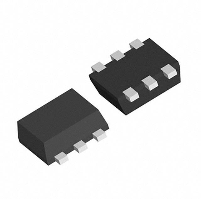
Since the package for these ICs are ultra small SC-82AB package and SON1612-6, high density mounting of
the ICs on board is possible.
FEATURES
• Supply current ....................................................................... Typ. 0.8µA (R313xx27x: VDD=3.0V)
• Operating Voltage Range...................................................... 0.8V to 6.0V (Topt=25°C)
• Detector Threshold................................................................ Setting with a step of 0.1V in the range of 1.0V
to 5.0V is possible. Further, 2.32V, 2.63V, 2.93V,
3.08V, 4.38V, and 4.63V can be provided as
standard.
• Embedded Power on Reset Delay Time Circuit.................... Typ. 240ms
• Detector Threshold Accuracy ................................................ ±2.0%
• Released Delay Time Accuracy ............................................ ±15.0%
• Temperature-Drift Coefficient of Detector Threshold ............ Typ. ±100ppm/°C
• Output Types ......................................................................... Nch Open Drain and CMOS
• Packages .............................................................................. SC-82AB, SON1612-6
APPLICATIONS
•
•
•
•
•
•
CPU and Logic Circuit Reset
Battery Checker
Window Comparator
Wave Shaping Circuit
Battery Back-up Circuit
Power Failure Detector
1
�∗ R3133Q (SC-82AB) is the discontinued product as of March, 2016.
R3132x/R3133x
BLOCK DIAGRAMS
2
R3132xxxEA Nch Open Drain Output
R3132xxxEC CMOS Output
R3133xxxEA Nch Open Drain Output
R3133xxxEC CMOS Output
�∗ R3133Q (SC-82AB) is the discontinued product as of March, 2016.
R3132x/R3133x
SELECTION GUIDE
The package type, the detector threshold, the output type and the taping type for the ICs can be selected at
the users’ request.
Quantity per
Product Name
Package
Pb Free
Halogen Free
Reel
R3132DxxE∗(y)-TR-FE
R3133DxxE∗(y)-TR-FE
SON1612-6
4,000 pcs
Yes
Yes
R3132QxxE∗(y)-TR-FE
SC-82AB
3,000 pcs
Yes
Yes
R3133QxxE∗(y)-TR-FE
xx : The detector threshold can be designated in the range from 1.0V(10) to 5.0V(50) in 0.1V steps.
y: If the detector threshold includes the 3rd digit, indicate the digit of 0.01V.
(2.32V, 2.63V, 2.93V, 3.08V, 4.38V, 4.63V)
Ex. If the detector threshold is 2.63V, R3132x26E∗3-TR-FE.
∗ : Designation of Output Type
(A) Nch Open Drain
(C) CMOS
3
�∗ R3133Q (SC-82AB) is the discontinued product as of March, 2016.
R3132x/R3133x
PIN CONFIGURATIONS
• SON1612-6
6
5
4
(mark side)
1
2
3
• SC-82AB
4
3
(mark side)
1
2
PIN DESCRIPTIONS
•
•
4
SON1612-6
Pin No
Symbol
1
VDD
2
GND
3
MR
4
OUT
5
GND
6
NC
Pin Description
Input Pin
Ground Pin
Manual Reset Input Pin
Active at “L” input. Pulled up via 1MΩ. If MR pin is not necessary,
open this node, or connect to VDD.
Output Pin
R3132D Series:"L" at detection
R3133D Series:"H" at detection
Ground Pin
No Connection
SC-82AB
Pin No
Symbol
1
GND
2
OUT
3
MR
4
VDD
Pin Description
Ground Pin
Output Pin
R3132Q Series :"L" at detection
R3133Q Series :"H" at detection
Manual Reset Input Pin
Active at "L" input. Pulled up via 1MΩ. If MR pin is not necessary,
open this node, or connect to VDD.
Input Pin
�∗ R3133Q (SC-82AB) is the discontinued product as of March, 2016.
R3132x/R3133x
ABSOLUTE MAXIMUM RATINGS
Symbol
VDD
VOUT
Item
Supply Voltage
Output Voltage (Nch Open Drain Output)
Rating
Unit
6.5
V
VSS−0.3 to 6.5
V
Output Voltage (CMOS Output)
VSS−0.3 to VDD+0.3
VMR
Input Voltage
VSS−0.3 to VDD+0.3
V
IOUT
Output Current
20
mA
Power Dissipation (SON1612-6)∗1, ∗2
500
Power Dissipation (SC-82AB)∗2
380
Topt
Operating Temperature Range
−40 to 85
°C
Tstg
Storage Temperature Range
−55 to 125
°C
PD
Tsolder
Soldering Temperature
mW
260°C, 10s
∗1) This specification is at mounted on board.
PD depends on conditions of mounting on board. This specification is based on the measurement at the
condition below:
∗Measurement Conditions
Environment: Mounted on board (Wind velocity 0m/s)
Board Material: FR-4 (2-layer)
Board dimensions : 40mm x 40mm x t1.6mm
Copper Area : 50%
∗2) For Power Dissipation, please refer to PACKAGE INFORMATION.
ABSOLUTE MAXIMUM RATINGS
Electronic and mechanical stress momentarily exceeded absolute maximum ratings may cause the
permanent damages and may degrade the life time and safety for both device and system using the device
in the field. The functional operation at or over these absolute maximum ratings is not assured.
5
�∗ R3133Q (SC-82AB) is the discontinued product as of March, 2016.
R3132x/R3133x
ELECTRICAL CHARACTERISTICS
Topt=25°C
Symbol
Item
Test Conditions
Min.
Topt=25°C
0.75
6.0
−40°C≤Topt≤85°C
0.85
6.0
Topt=25°C
0.80
6.0
−40°C≤Topt≤85°C
0.90
6.0
VDET×
0.98
VDET×
1.02
V
R3132
VDD
Operating Voltage
R3133
Typ.
Max.
Unit
V
VDET
Detector Threshold
ISS1
Supply Current1
VDD=VDET−0.1V, IOUT=0A
2.0
µA
ISS2
Supply Current2
VDD=VDET+0.1V, IOUT=0A
2.0
µA
Supply Current3
VDD=6.0V,
IOUT=0A
ISS3
VDET