RN5VD SERIES
LOW VOLTAGE DETECTOR WITH OUTPUT DELAY
NO. EA-027-160309
OUTLINE
The RN5VD Series are CMOS-based voltage detector ICs with high detector threshold accuracy and ultra-low
supply current, which can be operated at an extremely low voltage and is used for system reset as an example.
Each of these ICs consists of a voltage reference unit, a comparator, resistor net for detector threshold setting,
an output driver, a hysteresis circuit, and an output delay circuit. The detector threshold is fixed with high accuracy
internally and does not require any adjustment. Two output types, Nch open drain type and CMOS type are
available.
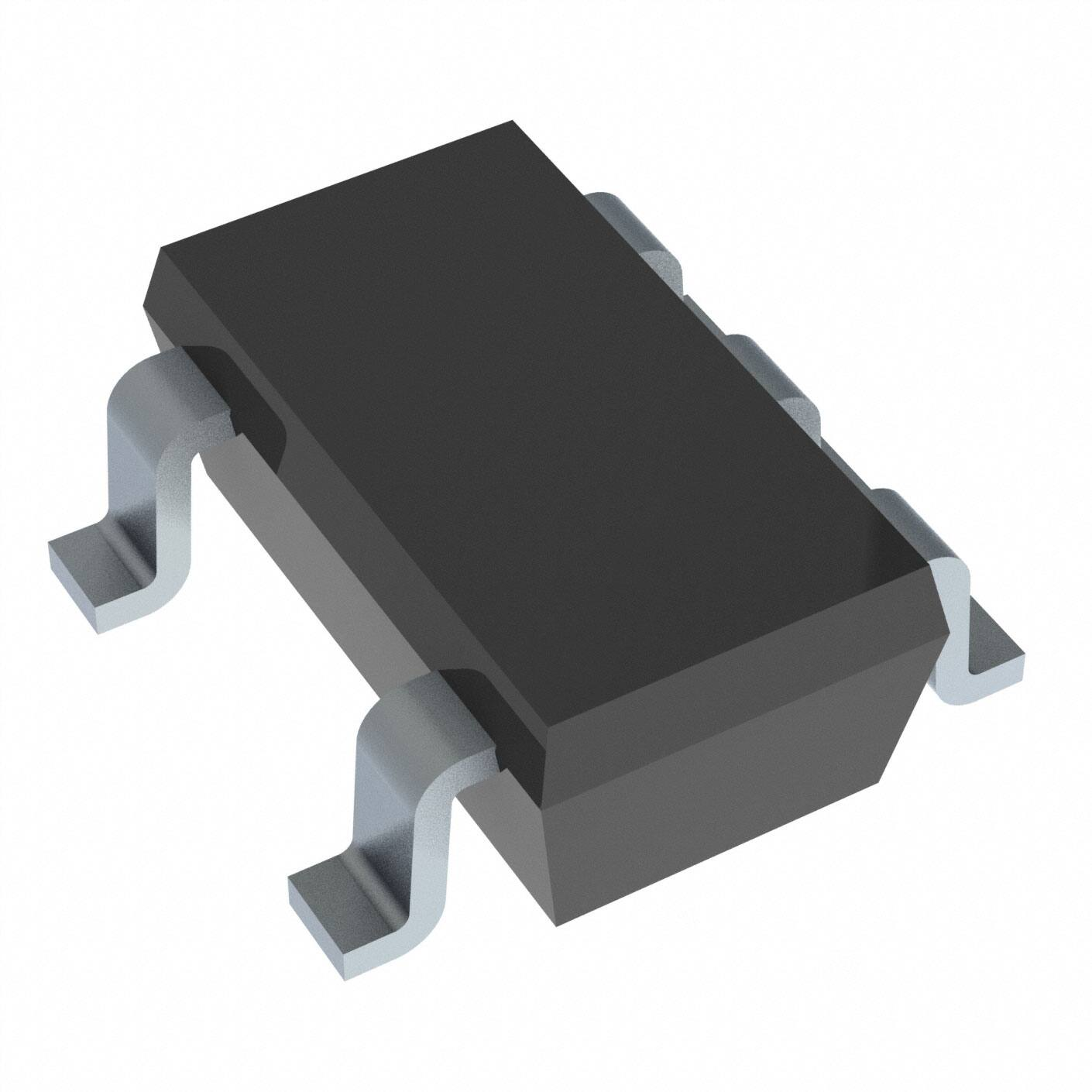
Since the package for these ICs is SOT-23-5 package, high density mounting of the ICs on board is possible.
FEATURES
•
•
•
•
•
•
•
•
Built-in Output Delay Circuit ............................................... Typ. 100ms with an external capacitor : 0.15µF
Supply Current ................................................................... Typ. 1.0µA (RN5VD15x, VDD=3.5V)
Operating Voltage Range................................................... 0.7 to 10.0V (Topt=25°C)
Detector Threshold Range ................................................. 0.9V to 6.0V (0.1V steps)
Detector Threshold Accuracy ............................................. ±2.5%
Temperature-Drift Coefficient of Detector Threshold ............Typ. ±100ppm/°C
Output Types ...................................................................... Nch Open Drain and CMOS
Package ............................................................................. SOT-23-5
APPLICATIONS
•
•
•
•
•
•
CPU and Logic Circuit Reset
Battery Checker
Window Comparator
Wave Shaping Circuit
Battery Back-up Circuit
Power Failure Detector
1
�RN5VD
BLOCK DIAGRAMS
RN5VDxxA
RN5VDxxC
OUT VDD
VDD
RD
RD
+
+
-
-
OUT
Vref
Vref
GND
GND
CD
CD
SELECTION GUIDE
The detector threshold, and the output type for the ICs can be selected at the users’ request.
Product Name
Package
Quantity per Reel
Pb Free
Halogen Free
RN5VDxx∗A-TR-FE
SOT-23-5
3,000 pcs
Yes
Yes
xx : The detector threshold can be designated in the range from 0.9V(09) to 6.0V(60) in 0.1V steps.
∗ : Designation of Output Type
(A) Nch Open Drain
(C) CMOS
2
�RN5VD
PIN CONFIGURATION
●SOT-23-5
5
4
(mark side)
1
2
3
PIN DESCRIPTION
Pin No.
Symbol
Pin Description
1
OUT
Output Pin("L" at Detection)
2
VDD
Input Pin
3
GND
4
NC
No Connection
5
CD
Pin for external capacitor ( for setting output delay)
Ground Pin
ABSOLUTE MAXIMUM RATINGS
Symbol
Item
Ratings
Unit
12
V
VDD
Supply Voltage
VOUT
Output Voltage
IOUT
Output Current
70
mA
PD
Power Dissipation (SOT-23-5)*
420
mW
Topt
Operating Temperature Range
−40 to +85
°C
Tstg
Storage Temperature Range
−55 to +125
°C
Tsolder
CMOS
VSS −0.3 to VDD+0.3
Nch
VSS −0.3~12
Lead Temperature (Soldering)
V
260°C 10s
* ) For Power Dissipation, please refer to PACKAGE INFORMATION.
ABSOLUTE MAXIMUM RATINGS
Electronic and mechanical stress momentarily exceeded absolute maximum ratings may cause the
permanent damages and may degrade the life time and safety for both device and system using the device
in the field. The functional operation at or over these absolute maximum ratings is not assured.
3
�RN5VD
ELECTRICAL CHARACTERISTICS
• RN5VD09A/C
Topt=25˚C
Symbol
Item
Conditions
Min.
Typ.
Max.
Unit.
–VDET
Detector Threshold
0.878
0.900
0.922
V
VHYS
Detector Threshold Hysteresis
0.027
0.045
0.063
V
VDD=0.8V
1.5
3.7
VDD=2.9V
0.9
2.7
ISS
VDDH
VDDL
µA
Supply Current
Maximum Operating Voltage
10
Minimum Operating Voltage
Topt=25˚C
0.55
0.70
–30˚C≤Topt≤85˚C
0.65
0.80
V
V
(Note 1)
VDS=0.05V, VDD=0.7V
0.01
0.05
VDS=0.5V, VDD=0.85V
0.05
0.50
VDS=–2.1V, VDD=4.5V
1.0
2.0
VDD=0.99V
0.297
0.495
VDS=0.1V, VDD=0.7V
2.0
30
VDS=0.5V, VDD=0.85V
10.0
100.0
0.5
1.0
Nch
IOUT
Output Current
Pch
VTCD
ICD
RD
∆–VDET
∆Topt
CD pin Threshold Voltage
mA
mA
0.693
V
µA
CD pin Sink Current
Delay Resistance
Detector Threshold
Temperature Coefficient
–30˚C≤Topt≤85˚C
±100
2.0
MΩ
ppm/˚C
(Note 1) Minimum Operating Voltage means the value of input voltage when output voltage maintains 0.1V or less, provided that in the case of Nch
Open Drain Type Products, the pull-up resistance is set at 470kΩ, and the pull-up voltage is set at 5.0V.
4
�RN5VD
• RN5VD18A/C
Topt=25˚C
Symbol
Item
Conditions
Min.
Typ.
Max.
Unit.
–VDET
Detector Threshold
1.755
1.800
1.845
V
VHYS
Detector Threshold Hysteresis
0.054
0.090
0.126
V
VDD=1.7V
2.5
5.0
VDD=3.8V
1.0
3.0
ISS
VDDH
VDDL
µA
Supply Current
Maximum Operating Voltage
Topt=25˚C
–30˚C≤Topt≤85˚C
Minimum Operating Voltage
(Note 1)
0.55
0.65
VDS=0.05V, VDD=0.7V
0.01
0.05
VDS=0.5V, VDD=1.5V
1.0
2.0
VDS=–2.1V, VDD=4.5V
1.0
2.0
VDD=1.98V
0.693
0.990
VDS=0.1V, VDD=0.7V
2.0
30
VDS=0.5V, VDD=1.5V
200.0
800.0
0.5
1.0
10
V
0.70
0.80
V
Nch
IOUT
Output Current
Pch
VTCD
ICD
RD
∆–VDET
∆Topt
CD pin Threshold Voltage
mA
mA
1.287
V
µA
CD pin Sink Current
Delay Resistance
Detector Threshold
Temperature Coefficient
–30˚C≤Topt≤85˚C
±100
2.0
MΩ
ppm/˚C
(Note 1) Minimum Operating Voltage means the value of input voltage when output voltage maintains 0.1V or less, provided that in the case of Nch
Open Drain Type Products, the pull-up resistance is set at 470kΩ, and the pull-up voltage is set at 5.0V.
5
�RN5VD
• RN5VD27A/C
Topt=25˚C
Symbol
Item
Conditions
Min.
Typ.
Max.
Unit.
–VDET
Detector Threshold
2.633
2.700
2.767
V
VHYS
Detector Threshold Hysteresis
0.081
0.135
0.189
V
VDD=2.6V
3.5
7.0
VDD=4.7V
1.1
3.3
ISS
VDDH
VDDL
µA
Supply Current
Maximum Operating Voltage
Topt=25˚C
–30˚C≤Topt≤85˚C
Minimum Operating Voltage
(Note 1)
0.55
0.65
VDS=0.05V, VDD=0.7V
0.01
0.05
VDS=0.5V, VDD=1.5V
1.0
2.0
VDS=–2.1V, VDD=4.5V
1.0
2.0
VDD=2.97V
1.188
1.485
VDS=0.1V, VDD=0.7V
2.0
30
VDS=0.5V, VDD=1.5V
200.0
800.0
0.5
1.0
10
V
0.70
0.80
V
Nch
IOUT
Output Current
Pch
VTCD
ICD
RD
∆–VDET
∆Topt
CD pin Threshold Voltage
mA
mA
1.782
V
µA
CD pin Sink Current
Delay Resistance
Detector Threshold
Temperature Coefficient
–30˚C≤Topt≤85˚C
±100
2.0
MΩ
ppm/˚C
( Note 1) Minimum Operating Voltage means the value of input voltage when output voltage maintains 0.1V or less, provided that in the case of Nch
Open Drain Type Products, the pull-up resistance is set at 470kΩ, and the pull-up voltage is set at 5.0V.
6
�RN5VD
• RN5VD36A/C
Topt=25˚C
Symbol
Item
Conditions
Min.
Typ.
Max.
Unit.
–VDET
Detector Threshold
3.510
3.600
3.690
V
VHYS
Detector Threshold Hysteresis
0.108
0.180
0.252
V
VDD=3.47V
4.5
9.0
VDD=5.6V
1.2
3.6
ISS
VDDH
VDDL
µA
Supply Current
Maximum Operating Voltage
0.55
0.65
Topt=25˚C
–30˚C≤Topt≤85˚C
Minimum Operating Voltage
(Note 1)
VDS=0.05V, VDD=0.7V
0.01
0.05
VDS=0.5V, VDD=1.5V
1.0
2.0
VDS=–2.1V, VDD=4.5V
1.0
2.0
VDD=3.96V
1.584
1.980
VDS=0.1V, VDD=0.7V
2.0
30
VDS=0.5V, VDD=1.5V
200.0
800.0
0.5
1.0
10
V
0.70
0.80
V
Nch
IOUT
Output Current
Pch
VTCD
ICD
RD
∆–VDET
∆Topt
CD pin Threshold Voltage
mA
mA
2.376
V
µA
CD pin Sink Current
Delay Resistance
Detector Threshold
Temperature Coefficient
–30˚C≤Topt≤85˚C
±100
2.0
MΩ
ppm/˚C
(Note 1) Minimum Operating Voltage means the value of input voltage when output voltage maintains 0.1V or less, provided that in the case of Nch
Open Drain Type Products, the pull-up resistance is set at 470kΩ, and the pull-up voltage is set at 5.0V.
7
�RN5VD
• RN5VD45A/C
Topt=25˚C
Symbol
Item
Conditions
Min.
Typ.
Max.
Unit.
–VDET
Detector Threshold
4.388
4.500
4.612
V
VHYS
Detector Threshold Hysteresis
0.135
0.225
0.315
V
VDD=4.34V
5.5
11.0
VDD=6.5V
1.3
3.9
ISS
VDDH
VDDL
µA
Supply Current
Maximum Operating Voltage
Topt=25˚C
–30˚C≤Topt≤85˚C
Minimum Operating Voltage
(Note 1)
0.55
0.65
VDS=0.05V, VDD=0.7V
0.01
0.05
VDS=0.5V, VDD=1.5V
1.0
2.0
VDS=–2.1V, VDD=8.0V
1.5
3.0
VDD=4.95V
1.980
2.475
VDS=0.1V, VDD=0.7V
2.0
30
VDS=0.5V, VDD=1.5V
200.0
800.0
0.5
1.0
10
V
0.70
0.80
V
Nch
IOUT
Output Current
Pch
VTCD
ICD
RD
∆–VDET
∆Topt
CD pin Threshold Voltage
mA
mA
2.970
V
µA
CD pin Sink Current
Delay Resistance
Detector Threshold
Temperature Coefficient
–30˚C≤Topt≤85˚C
±100
2.0
MΩ
ppm/˚C
(Note 1) Minimum Operating Voltage means the value of input voltage when output voltage maintains 0.1V or less, provided that in the case of Nch
Open Drain Type Products, the pull-up resistance is set at 470kΩ, and the pull-up voltage is set at 5.0V.
8
�RN5VD
• RN5VD54A/C
Topt=25˚C
Symbol
Item
Conditions
Min.
Typ.
Max.
Unit.
–VDET
Detector Threshold
5.265
5.400
5.535
V
VHYS
Detector Threshold Hysteresis
0.162
0.270
0.378
V
VDD=5.2V
6.0
12.0
VDD=7.4V
1.4
4.2
ISS
VDDH
VDDL
µA
Supply Current
Maximum Operating Voltage
Topt=25˚C
–30˚C≤Topt≤85˚C
Minimum Operating Voltage
(Note 1)
0.55
0.65
VDS=0.05V, VDD=0.7V
0.01
0.05
VDS=0.5V, VDD=1.5V
1.0
2.0
1.5
3.0
VDD=5.94V
2.376
2.970
VDS=0.1V, VDD=0.7V
2.0
30
VDS=0.5V, VDD=1.5V
200.0
800.0
0.5
1.0
10
V
0.70
0.80
V
Nch
IOUT
Output Current
Pch
VTCD
ICD
RD
∆–VDET
∆Topt
CD pin Threshold Voltage
mA
VDS=–2.1V, VDD=8.0V
mA
3.564
V
µA
CD pin Sink Current
Delay Resistance
Detector Threshold
Temperature Coefficient
–30˚C≤Topt≤85˚C
±100
2.0
MΩ
ppm/˚C
(Note 1) Minimum Operating Voltage means the value of input voltage when output voltage maintains 0.1V or less, provided that in the case of Nch
Open Drain Type Products, the pull-up resistance is set at 470kΩ, and the pull-up voltage is set at 5.0V.
9
�RN5VD
ELECTRICAL CHARACTERISTICS BY DETECTOR THRESHOLD
• RN5VD09A/C to RN5VD39A/C
Part Number.
Detector Threshold
Hysteresis
–VDET (V)
VHYS (V)
Supply Current 1 Supply Current 2 Output Current 1
Iss1 (µA)
Iss2 (µA)
IOUT1 (mA)
Min. Typ. Max. Min. Typ. Max. condi- Typ. Max. condi- Typ. Max. condi- Min. Typ.
tions
tions
tions
RN5VD09A/C 0.878 0.900 0.922 0.027 0.045 0.063
RN5VD10A/C 0.975 1.000 1.025 0.030 0.050 0.070
RN5VD11A/C 1.073 1.100 1.127 0.033 0.055 0.077
RN5VD12A/C 1.170 1.200 1.230 0.036 0.060 0.084
RN5VD13A/C 1.268 1.300 1.332 0.039 0.065 0.091
RN5VD14A/C 1.365 1.400 1.435 0.042 0.070 0.098
1.5
3.7
1.8
4.5
2.0
5.0
0.9
IOUT2 (mA)
conditions
2.7
Min. Typ.
VDD=
0.05 0.50
0.85V
VDD=
0.2
1.0V
1.0
RN5VD15A/C 1.463 1.500 1.537 0.045 0.075 0.105
Output Current 2
1.0
3.0
RN5VD16A/C 1.560 1.600 1.640 0.048 0.080 0.112
RN5VD17A/C 1.658 1.700 1.742 0.051 0.085 0.119
2.5
5.0
3.0
6.0
RN5VD18A/C 1.755 1.800 1.845 0.054 0.090 0.126
VDD=
(–VDET)
RN5VD20A/C 1.950 2.000 2.050 0.060 0.100 0.140 –0.10V
RN5VD21A/C 2.048 2.100 2.152 0.063 0.105 0.147
RN5VD19A/C 1.853 1.900 1.947 0.057 0.095 0.133
RN5VD22A/C 2.145 2.200 2.255 0.066 0.110 0.154
RN5VD23A/C 2.243 2.300 2.357 0.069 0.115 0.161
Nch
VDD=
(–VDET)
+2.0V 1.1
RN5VD24A/C 2.340 2.400 2.460 0.072 0.120 0.168
RN5VD25A/C 2.438 2.500 2.562 0.075 0.125 0.175
3.3
VDD=
0.7V
RN5VD26A/C 2.535 2.600 2.665 0.078 0.130 0.182
RN5VD27A/C 2.633 2.700 2.767 0.081 0.135 0.189
3.5
7.0
4.0
8.0
RN5VD28A/C 2.730 2.800 2.870 0.084 0.140 0.196
RN5VD29A/C 2.828 2.900 2.972 0.087 0.145 0.203
RN5VD30A/C 2.925 3.000 3.075 0.090 0.150 0.210
RN5VD31A/C 3.023 3.100 3.177 0.093 0.155 0.217
RN5VD32A/C 3.120 3.200 3.280 0.096 0.160 0.224
RN5VD33A/C 3.218 3.300 3.382 0.099 0.165 0.231
RN5VD34A/C 3.315 3.400 3.485 0.102 0.170 0.238 VDD=
(–VDET)
1.2
RN5VD35A/C 3.413 3.500 3.587 0.105 0.175 0.245 –0.13V
RN5VD36A/C 3.510 3.600 3.690 0.108 0.180 0.252
RN5VD37A/C 3.608 3.700 3.792 0.111 0.185 0.259
RN5VD38A/C 3.705 3.800 3.895 0.114 0.190 0.266
RN5VD39A/C 3.803 3.900 3.997 0.117 0.195 0.273
(Note) Refer to the previously defined “Minimum Operating Voltage”.
Condition 1 : Topt=25˚C
Condition 2 : –30˚C≤Topt≤85˚C
10
VDS=
0.05V 0.01 0.05
4.5
9.0
3.6
Nch
VDS=
0.5V
VDD=
1.5V 1.0
2.0
�RN5VD
Topt=25˚C
Output Current 3
IOUT3 (mA)
condi- Min. Typ.
tions
Minimum Oper- CD Pin Threshold Voltage
ating Voltage
VDDL (V)
Typ.
VTCD (V)
CD Pin Output
Current 1
ICD1 (µA)
Max. condi- Min. Typ. Max. condi- Min. Typ.
tions
tions
CD Pin Output Current 2
Delay
Resistance
Detector
Threshold
Tempco.
ICD2 (µA)
RD (MΩ)
∆–VDET (ppm/˚C)
∆Topt
conditions
VDD × VDD × VDD ×
0.3 0.5 0.7
Min. Typ. Min. Typ. Max. conditions
VDD=
0.85V
10
100
VDD=
1.0V
50
200
Typ.
VDD × VDD × VDD ×
0.35 0.5 0.65
Pch
(Note1) (Note1)
VDS =
0.1V
Condition1 Condition1
VDS=
–2.1V 1.0
VDD=
4.5V
0.70 VDD=
(–VDET)
2.0
Condition2 Condition2 × 1.1V
0.65 0.80
0.55
VDD =
0.7V
2.0
30
VDS =
0.5V
0.5
VDD =
1.5V 200
1.0
2.0
–30˚C≤
Topt
≤85˚C ±100
800
VDD × VDD × VDD ×
0.4 0.5 0.6
11
�RN5VD
• RN5VD40A/C to RN5VD60A/C
Part Number.
Detector Threshold
Hysteresis
–VDET (V)
VHYS (V)
Supply Current 1 Supply Current 2 Output Current 1
Iss1 (µA)
Iss2 (µA)
Output Current 2
IOUT1 (mA)
Min. Typ. Max. Min. Typ. Max. condi- Typ. Max. condi- Typ. Max. condi- Min. Typ.
tions
tions
tions
IOUT2 (mA)
conditions
Min. Typ.
RN5VD40A/C 3.900 4.000 4.100 0.120 0.200 0.280
RN5VD41A/C 3.998 4.100 4.202 0.123 0.205 0.287
RN5VD42A/C 4.095 4.200 4.305 0.126 0.210 0.294
5.0
10.0
RN5VD43A/C 4.193 4.300 4.407 0.129 0.215 0.301
RN5VD44A/C 4.290 4.400 4.510 0.132 0.220 0.308 VDD=
(–VDET)
1.3
RN5VD45A/C 4.388 4.500 4.612 0.135 0.225 0.315 –0.16V
RN5VD46A/C 4.485 4.600 4.715 0.138 0.230 0.322
RN5VD47A/C 4.583 4.700 4.817 0.141 0.235 0.329
5.5
3.9
11.0
Nch
RN5VD48A/C 4.680 4.800 4.920 0.144 0.240 0.336
RN5VD49A/C 4.778 4.900 5.022 0.147 0.245 0.343
VDD=
(–VDET)
+2.0V
RN5VD50A/C 4.875 5.000 5.125 0.150 0.250 0.350
RN5VD51A/C 4.973 5.100 5.227 0.153 0.255 0.357
RN5VD52A/C 5.070 5.200 5.330 0.156 0.260 0.364
6.0
VDS=
0.05V 0.01 0.05
VDD=
0.7V
12.0
RN5VD53A/C 5.168 5.300 5.432 0.159 0.265 0.371
RN5VD54A/C 5.265 5.400 5.535 0.162 0.270 0.378 VDD=
RN5VD55A/C 5.363 5.500 5.637 0.165 0.275 0.385 (–VDET)
1.4
RN5VD56A/C 5.460 5.600 5.740 0.168 0.280 0.392 –0.20V
RN5VD57A/C 5.558 5.700 5.842 0.171 0.285 0.399
RN5VD58A/C 5.655 5.800 5.945 0.174 0.290 0.406
RN5VD59A/C 5.753 5.900 6.047 0.177 0.295 0.413
RN5VD60A/C 5.850 6.000 6.150 0.180 0.300 0.420
(Note) Refer to the previously defined “Minimum Operating Voltage”.
Condition 1 : Topt=25˚C
Condition 2 : –30˚C≤Topt≤85˚C
12
6.5
13.0
4.2
Nch
VDD=
1.0
VDS= 1.5V
0.5V
2.0
�RN5VD
Topt=25˚C
OperOutput Current 3 Minimum
ating Voltage CD Pin Threshold Voltage
IOUT3 (mA)
condi- Min. Typ.
tions
Pch
VDDL (V)
Typ.
VTCD (V)
(Note1) (Note1)
0.55
0.70
3.0
Condition2 Condition2
VDD=
8.0V
0.65
CD Pin Output Current 2
Delay
Resistance
ICD1 (µA)
IOUT1 (mA)
IOUT2 (mA)
∆–VDET (ppm/˚C)
∆Topt
Max. condi- Min. Typ. Max. condi- Min. Typ.
tions
tions
Condition1 Condition1
VDS=
–2.1V 1.5
CD Pin Output
Current 1
Detector
Threshold
Tempco.
0.80
VDD=
VDS=
0.1V
VDD × VDD × VDD ×
(–VDET)
2.0
DD=
× 1.1V 0.4 0.5 0.6V V0.7V
30
conditions
Min. Typ. condi- Typ. Max. conditions
tions
VDS= VDD=
0.5V 1.5V 200
800
0.5
1.0
2.0
–30˚C≤
Topt
≤85˚C
Typ.
±100
13
�RN5VD
OPERATION
VDD
Current Source
Ra Comparator
–
RD
Pch
Schmitt Trigger
+
OUT
Rb
Vref
Tr.2
Tr.1
Nch
Rc
GND
CD
Output Capacitor
Fig. 1 Block Diagram
1
2
3
5
B
Released Voltage +VDET
Detected Voltage –VDET
4
A
Step
Step 1
Step 2
Step 3
Step 4
Step 5
Comparator (–) Pin
Input Voltage
I
II
II
II
I
Comparator Output
L
H
Indefinite
H
L
Tr. 1, 2
OFF
ON
Indefinite
ON
OFF
Nch
OFF
ON
Indefinite
ON
OFF
Pch
ON
OFF
Indefinite
OFF
ON
Detector Threshold Hysteresis
Supply Voltage
(VDD)
Minimum Operaing Voltage
GND
Output Tr.
Output Voltage
(OUT)
Delay Time
I.
GND
II.
Rb + Rc
Ra + Rb + Rc
Rb
Ra + Rb
· VDD
· VDD
Fig. 2 Operation Diagram
Step 1. Output voltage is equal to pull-up voltage.
Step 2. When input voltage (VDD) reaches the state of Vref≥VDD · (Rb+Rc) / (Ra+Rb+Rc) at point A (Detected Voltage –VDET) , the output of comparator is
reversed, so that output voltage becomes GND. Discharging is performed from CD pin connected to an external capacitor. No delay time is generated.
Step 3. Output voltage becomes indefinite when power source voltage(VDD) is smaller than minimum operating voltage. When the output is pulled up, VDD is
output.
Step 4. Output voltage becomes equal to GND.
Step 5. When input voltage (VDD) reaches the state of Vref≤VDD · Rb/ (Ra+Rb) at Point B (Released Voltage +VDET) , the output of comparator is reversed,
and the external capacitor is charged through CD pin, so that output voltage becomes equal to pulled-up voltage after a delay time tD (=0.69× 10⁶× CD) .
14
�RN5VD
• Output Delay Operation
Supply Voltage
(VDD)
CD pin Voltage
Released Voltage (+VDET)
CD pin Threshold Voltage (VTCD)
GND
Output Voltage
(OUT)
GND
Output Delay Time (tD)
When the supply voltage crosses the released voltage (+VDET) from a low value to a value higher than
the released voltage (+VDET) , the CD pin voltage starts to increase (starts to charge the external capacitor).
The output voltage is maintained at “L” level until the CD pin voltage reaches to VTCD (CD pin threshold
voltage) after that the output voltage is reversed to “H”.
The time period from beginning of charging capacitor to output voltage reversing represents the output delay (tD) .
• Output Delay Time
Delay time (tD) can be set accordance with the capacitance CD of external capacitor as below
tD=0.69 × 10 6× CD (s)
15
�RN5VD
TEST CIRCUITS
ISS
+5V or VDD
VDD
VDD
470kΩ
VIN
VIN
RN5VD
SERIES
RN5VD
SERIES
GND
GND
Fig. 3 Supply Current test Circuit
Fig. 4 Detector Threshold Test Circuit
VDD
VDD
VIN
IOUT
VIN
RN5VD
SERIES
OUT
OUT
RN5VD××C
SERIES
VDS
GND
IOUT
OUT
VDD+VDS
GND
Fig. 5 Nch Driver Output Current Test Circuit
Fig. 6 Pch Driver Output Current Test Circuit
+5V or VDD
VDD
VDD
VIN
CD
RN5VD
SERIES
VDS
VIN
470kΩ
ICD
OUT
CD
OUT
VDS
GND
GND
Fig. 7 CD pin Threshold Voltage Test Circuit
Fig. 8 CD pin Sink Current Test Circuit
+VDET+2.0V
+5V
VDD
Input Voltage
CD
VIN
0.7V
CD
GND
RN5VD
SERIES
470kΩ
OUT
GND
100%
Output Voltage
50%
Fig. 9 Output Delay Time Test Circuit
GND
tPHL
*) at Fig.4,7,9. CMOS Output Type does not
need a pull-up resistor.
16
tD
RN5VD
SERIES
�RN5VD
TYPICAL CHARACTERISTICS
1) Supply Current vs. Input Voltage
RN5VD09x
RN5VD27x
5
2.5
Supply Current Iss(µA)
Supply Current Iss(µA)
3.0
Topt=80˚C
2.0
25˚C
1.5
–30˚C
1.0
0.5
0
4
3
Topt=80˚C
2
25˚C
1
–30˚C
0
0
2
4
6
8
10
8
10
0
2
Input Voltage VIN(V)
4
6
8
Input Voltage VIN(V)
10
RN5VD45x
8
Supply Current Iss(µA)
7
Topt=80˚C
6
25˚C
5
4
3
–30˚C
2
1
0
0
2
4
6
Input Voltage VIN(V)
2) Detector Threshold vs. Temperature
RN5VD27x
RN5VD09x
2.90
Detector Threshold VDET(V)
Detector Threshold VDET(V)
0.98
0.96
+VDET
0.94
0.92
–VDET
0.90
0.88
0.86
–40
–20
0
20
40
60
Temperature Topt(˚C)
80
2.85
+VDET
2.80
2.75
–VDET
2.70
2.65
2.60
–40
–20
0
20
40
60
Temperature Topt(˚C)
80
17
�RN5VD
RN5VD45x
Detector Threshold VDET(V)
4.9
4.8
+VDET
4.7
4.6
–VDET
4.5
4.4
–40
–20
0
20
40
Temperature Topt(˚C)
60
80
3) Output Voltage vs. Input Voltage
RN5VD09A
0.8
0.6
Topt=80˚C
0.4
25˚C
–30˚C
0.2
5
0
4
25˚C
3
2
1
0.2
0.4
0.6
0.8
0
1
0.2
RN5VD27A
3.0
VDD Pull-up
470kΩ
2.0
1.5
1.0
Topt= –30˚C
0
0.5
1.0
1.5
2.0
Input Voltage VIN(V)
0.8
1.0
6
5V Pull-up
470kΩ
5
Topt=–30˚C
4
25˚C
3
2
80˚C
1
25˚C
80˚C
0
0.6
RN5VD27A
Output Voltage VOUT(V)
2.5
0.5
0.4
Input Voltage VIN(V)
Input Voltage VIN(V)
Output Voltage VOUT(V)
–30˚C
Topt=80˚C
0
0
18
5V Pull-up
470kΩ
RN5VD09A
6
Output Voltage VOUT(V)
Output Voltage VOUT(V)
1.0
VDD Pull-up
470kΩ
0
2.5
3.0
0
0.5
1.0
1.5
2.0
Input Voltage VIN(V)
2.5
3.0
�RN5VD
VDD Pull-up
470kΩ
RN5VD45A
6
Output Voltage VOUT(V)
Output Voltage VOUT(V)
5
4
3
2
1
25˚C
80˚C
0
5
Topt= –30˚C
4
25˚C
3
80˚C
2
1
Topt= –30˚C
0
5V Pull-up
470kΩ
RN5VD45A
0
1
2
3
4
0
5
1
2
3
4
5
Input Voltage VIN(V)
Input Voltage VIN(V)
4) Nch Driver Output Current vs. VDS
RN5VD09x
0.45
Output Currert IOUT(mA)
0.40
VDD=0.85V
0.35
0.30
0.25
0.20
0.15
0.10
0.7V
14
VDD=2.5V
12
10
8
2.0V
6
4
1.5V
2
0.05
0
0
0
0.2
0.4
0.6
VDS(V)
0.8
1.0
0
0.5
1.0
1.5
VDS(V)
2.0
2.5
RN5VD45x
40
Output Currert IOUT(mA)
Output Currert IOUT(mA)
RN5VD27x
16
35
VDD=4.0V
30
3.5V
25
20
3.0V
15
2.5V
10
2.0V
5
1.5V
0
0
1
2
VDS(V)
3
4
19
�RN5VD
5) Nch Driver Output Current vs. Input Voltage
RN5VD09x
VDS=0.5V
0.7
VDS=0.5V
10
Output Current IOUT(mA)
Output Current IOUT(mA)
0.6
RN5VD27x
12
0.5
0.4
Topt = 80˚C
0.3
25˚C
0.2
0.1
Topt = –30˚C
25˚C
8
6
80˚C
4
2
–30˚C
0
0
0
0.2
RN5VD45x
18
Output Current IOUT(mA)
0.4
0.6
0.8
Input Voltage VIN(V)
1.0
0
0.5
1.0
1.5
2.0
Input Voltage VIN(V)
2.5
3.0
VDS=0.5V
16
14
Topt = – 30˚C
25˚C
12
10
8
80˚C
6
4
2
0
0
1
2
3
Input Voltage VIN(V)
4
5
6) Pch Driver Output Current vs. Input Voltage
RN5VD09C
RN5VD27C
4.0
4.0
VDS = –2.1V
3.0
Output Current IOUT(mA)
Output Current IOUT(mA)
VDS = –2.1V
3.5
–1.5V
2.5
–1.0V
2.0
1.5
–0.5V
1.0
0.5
3.0
–1.5V
2.5
2.0
–1.0V
1.5
–0.5V
1.0
0.5
0
0
0
20
3.5
2
4
6
Input Voltage VIN(V)
8
10
0
2
4
6
Input Voltage VIN(V)
8
10
�RN5VD
RN5VD45C
4.0
VDS =–2.1V
Output Current IOUT(mA)
3.5
3.0
–1.5V
2.5
–1.0V
2.0
1.5
–0.5V
1.0
0.5
0
0
2
4
6
Input Voltage VIN(V)
8
10
7) CD pin Threshold Voltage vs. Temperature
0.7
0.6
0.5
0.4
0.3
0.2
–40
–20
0
20
40
Temperature Topt(˚C)
RN5VD45x
CD pin Threshold Voltage VTCD(V)
RN5VD27x
VDD=0.99V
CD pin Threshold Voltage VTCD(V)
CD pin Threshold Voltage VTCD(V)
RN5VD09x
0.8
2.8
60
80
1.8
VDD=2.97V
1.7
1.6
1.5
1.4
1.3
1.2
–40
–20
0
20
40
Temperature Topt(˚C)
60
80
VDD=4.95V
2.7
2.6
2.5
2.4
2.3
2.2
–40
–20
0
20
40
60
Temperature Topt(˚C)
80
21
�RN5VD
8) CD pin Sink Current vs. Input Voltage
RN5VD09x
VDS=0.5V
CD pin Sink Current ICD(mA)
CD pin Sink Current ICD(mA)
VDS=0.5V
Topt = –30˚C
0.16
0.14
0.12
0.10
0.08
Topt = 80˚C
0.06
25˚C
0.04
0.02
2.5
25˚C
2.0
1.5
80˚C
1.0
0.5
–30˚C
0
0
0
0.2
0.4
0.6
0.8
Input Voltage VIN(V)
RN5VD45x
5
CD pin Sink Current ICD(mA)
RN5VD27x
3.0
0.18
0
1.0
0.5
1.0
1.5
2.0
Input Voltage VIN(V)
2.5
3.0
VDS=0.5V
4
Topt = –30˚C
25˚C
3
2
80˚C
1
0
0
1
2
3
Input Voltage VIN(V)
4
5
9) CD pin Sink Current vs. CD pin Voltage
RN5VD09x
CD pin Sink Current ICD(mA)
CD pin Sink Current ICD(mA)
0.10
VDD = 0.85V
0.08
0.06
0.04
0.7V
0.02
0
3.5
VDD = 2.5V
3.0
2.5
2.0
2.0V
1.5
1.0
1.5V
0.5
0
0
22
RN5VD27x
4.0
0.12
0.2
0.4
0.6
0.8
CD pin Voltage VCD(V)
1.0
0
0.5
1.0
1.5
2.0
CD pin Voltage VDS(V)
2.5
�RN5VD
RN5VD45x
CD pin Sink Current ICD(mA)
10
VDD = 4.0V
8
3.5V
6
3.0V
4
2.5V
2
2.0V
1.5V
0
0
1
2
3
CD pin Voltage VDS(V)
4
10) Output delay Time vs. External Capacitance
RN5VD09A
100
10
tD
1
tPHL
0.1
0.01
0.0001
0.001
0.01
RN5VD27A
1000
Output Delay Time tP(ms)
Output Delay Time tP(ms)
1000
0.1
100
10
tD
1
tPHL
0.1
0.01
0.0001
1
0.001
0.01
0.1
External Capacitance CD(µF)
External Capacitance CD(µF)
1
11) Delay Resistance vs. Temperature
RN5VD45A
1000
RN5VDxxx
100
Delay Resistance RD(MΩ)
Output Delay Time tP(ms)
1.6
10
tD
1
tPHL
0.1
0.01
0.0001
0.001
0.01
0.1
External Capacitance CD(µF)
1
1.4
1.2
1.0
0.8
0.6
0.4
–40
–20
0
20
40
60
80
Temperature Topt(˚C)
23
�RN5VD
TYPICAL APPLICATIONS
• RN5VDxxA CPU Reset Circuit (Nch Open Drain Output)
(1) Input Voltage to RN5VDxxA is
the same as the input voltage to CPU.
(2) Input Voltage to RN5VDxxA is
different from the input voltage to CPU.
VDD
VDD
CD
CD
R
RN5VDxxA
SERIES
VDD1
VDD2
VDD
RESET
OUT
VDD
CD
CPU
GND
CD
GND
R
RN5VDxxA
SERIES
RESET
OUT
GND
• RN5VDxxC CPU Reset Circuit (CMOS Output)
VDD
VDD
CD
CD
VDD
RN5VDxxC
SERIES
RESET
OUT
CPU
GND
GND
• Memory Back-up Circuit
VDD
VCC
D1
D2
A Y1
Y2
B
Y3
G Y4
GND
VDD
CD
RN5VDxxC
SERIES
CD
GND
24
OUT
VDD
VCC
VCC
VCC
VCC
RAM1
RAM2
RAM3
RAM4
GND CS
GND CS
GND CS
GND CS
CPU
GND
�RN5VD
• Manual Reset Circuit
VDD
VDD
VDD
VDD
R
CD
RN5VDxxA
SERIES
CD
OUT
CD
RN5VDxxC
SERIES
OUT
CD
GND
GND
TECHNICAL NOTES
When connecting resistors to the device’s input pin
When connecting a resistor (R1) to an input of this device, the input voltage decreases by [Device’s
Consumption Current] x [Resistance Value] only. And, the cross conduction current*1, which occurs when
changing from the detecting state to the release state, is decreased the input voltage by [Cross Conduction
Current] x [Resistance Value] only. And then, this device will enter the re-detecting state if the input voltage
reduction is larger than the difference between the detector voltage and the released voltage.
When the input resistance value is large and the VDD is gone up at mildly in the vicinity of the released voltage,
repeating the above operation may result in the occurrence of output.
As shown in Figure A/B, set R1 to become 100 kΩ or less as a guide, and connect CIN of 0.1 μF and more to
between the input pin and GND. Besides, make evaluations including temperature properties under the actual
usage condition, with using the evaluation board like this way. As a result, make sure that the cross conduction
current has no problem.
R1
R1
VDD
CIN
*2
Voltage
Detector
VDD
OUT pin
R2
CIN
*2
GND
Figure A
Voltage
Detector
OUT pin
GND
Figure B
*1 In the CMOS output type, a charging current for OUT pin is included.
*2 Note the bias dependence of capacitors.
25
�1. The products and the product specifications described in this document are subject to change or discontinuation of
production without notice for reasons such as improvement. Therefore, before deciding to use the products, please
refer to Ricoh sales representatives for the latest information thereon.
2. The materials in this document may not be copied or otherwise reproduced in whole or in part without prior written
consent of Ricoh.
3. Please be sure to take any necessary formalities under relevant laws or regulations before exporting or otherwise
taking out of your country the products or the technical information described herein.
4. The technical information described in this document shows typical characteristics of and example application circuits
for the products. The release of such information is not to be construed as a warranty of or a grant of license under
Ricoh's or any third party's intellectual property rights or any other rights.
5. The products listed in this document are intended and designed for use as general electronic components in standard
applications (office equipment, telecommunication equipment, measuring instruments, consumer electronic products,
amusement equipment etc.). Those customers intending to use a product in an application requiring extreme quality
and reliability, for example, in a highly specific application where the failure or misoperation of the product could result
in human injury or death (aircraft, spacevehicle, nuclear reactor control system, traffic control system, automotive and
transportation equipment, combustion equipment, safety devices, life support system etc.) should first contact us.
6. We are making our continuous effort to improve the quality and reliability of our products, but semiconductor products
are likely to fail with certain probability. In order to prevent any injury to persons or damages to property resulting from
such failure, customers should be careful enough to incorporate safety measures in their design, such as redundancy
feature, fire containment feature and fail-safe feature. We do not assume any liability or responsibility for any loss or
damage arising from misuse or inappropriate use of the products.
7. Anti-radiation design is not implemented in the products described in this document.
8. The X-ray exposure can influence functions and characteristics of the products. Confirm the product functions and
characteristics in the evaluation stage.
9. WLCSP products should be used in light shielded environments. The light exposure can influence functions and
characteristics of the products under operation or storage.
10. There can be variation in the marking when different AOI (Automated Optical Inspection) equipment is used. In the
case of recognizing the marking characteristic with AOI, please contact Ricoh sales or our distributor before attempting
to use AOI.
11. Please contact Ricoh sales representatives should you have any questions or comments concerning the products or
the technical information.
Halogen Free
Ricoh is committed to reducing the environmental loading materials in electrical devices
with a view to contributing to the protection of human health and the environment.
Ricoh has been providing RoHS compliant products since April 1, 2006 and Halogen-free products since
April 1, 2012.
http://www.e-devices.ricoh.co.jp/en/
Sales & Support Offices
RICOH ELECTRONIC DEVICES CO., LTD.
Higashi-Shinagawa Office (International Sales)
3-32-3, Higashi-Shinagawa, Shinagawa-ku, Tokyo 140-8655, Japan
Phone: +81-3-5479-2857 Fax: +81-3-5479-0502
RICOH EUROPE (NETHERLANDS) B.V.
Semiconductor Support Centre
Prof. W.H. Keesomlaan 1, 1183 DJ Amstelveen, The Netherlands
Phone: +31-20-5474-309
RICOH INTERNATIONAL B.V. - German Branch
Semiconductor Sales and Support Centre
Oberrather Strasse 6, 40472 Düsseldorf, Germany
Phone: +49-211-6546-0
RICOH ELECTRONIC DEVICES KOREA CO., LTD.
3F, Haesung Bldg, 504, Teheran-ro, Gangnam-gu, Seoul, 135-725, Korea
Phone: +82-2-2135-5700 Fax: +82-2-2051-5713
RICOH ELECTRONIC DEVICES SHANGHAI CO., LTD.
Room 403, No.2 Building, No.690 Bibo Road, Pu Dong New District, Shanghai 201203,
People's Republic of China
Phone: +86-21-5027-3200 Fax: +86-21-5027-3299
RICOH ELECTRONIC DEVICES CO., LTD.
Taipei office
Room 109, 10F-1, No.51, Hengyang Rd., Taipei City, Taiwan (R.O.C.)
Phone: +886-2-2313-1621/1622 Fax: +886-2-2313-1623
�


 工商网监
湘ICP备2023018690号
工商网监
湘ICP备2023018690号

