Power Management IC Series for Automotive Body Control
Motor Driver
No.09039EAT02
BD6941FM
●Description
BD6941FM is the reversible motor driver for output 1.25A (1Motor), and can control a DC motor in four modes (Forward,
Reverse, Standby, Brake) corresponding to two control logic inputs.
●Features
1) 1ch DMOS H bridge output
2) Four output states ( Forward,Reverse,Standby,Brake ) by two control logic
3) Built-in surge-absorbing diodes
4) Low standby current
5) Output overcurrent protection with timer.
6) Over voltage detection switch off
7) TSD detects junction temperature and circuitry switches off the outputs at high temperature.
8) Built-in protection monitor pin (PO)
●Applications
Onboard devices(Vehicle equipment etc)
●Absolute Maximum Ratings(Ta=25℃)
PARAMETER
SUPPLY VOLTAGE
INPUT VOLTAGE
SYMBOL
LIMIT
UNIT
Vcc
50
V
VINP, VINN
-0.3~20
V
OUTPUT CURRENT
IO
1.25
(*1)
A
POWER DISSIPATION
Pd
2.8
(*2)
W
OPERATING TEMPERATURE
Topr
-40~105
℃
STORAGE TEMPERATURE
Tstg
-55~150
℃
JUNCTION TEMPERATURE
Tjmax
150
℃
*1 Not to exceed Pd and ASO.
*2 Mounted on a glass epoxy PCB (70mm×70mm×1.6mm).
To use at temperature above Ta=25℃ reduce 22.4mW/℃.
●Operating Range
PARAMETER
SUPPLY VOLTAGE
www.rohm.com
© 2009 ROHM Co., Ltd. All rights reserved.
SYMBOL
LIMIT
UNIT
Vcc
8.0~16.0
V
1/8
2009.06 - Rev.A
�Technical Note
BD6941FM
●Electrical Characteristics(Unless otherwise specified, Vcc=8V~16V, Ta=-40℃~105℃)
LIMIT
PARAMETER
SYMBOL
UNIT
CONDITIONS
MIN.
TYP.
MAX
Circuit current 1
Icc1
0
10
μA
Standby mode
Circuit current 2
Icc2
3
8
mA
Forward or reverse mode
Circuit current 3
Icc3
3
8
mA
Brake mode
Input Voltage “H” level
VIH
3.0
V
Input Voltage “L” level
VIL
1.0
V
“H” level input current
IIH
50
100
μA
VIN=5.0V, flowing in current
“L” level input current
IIL
0
10
μA
VIN=0V, flowing out current
Output on voltage 1
VON1
0.84
1.5
V
Vcc=12V, Iout =0.5A, total drop
Vcc=8~16V, Iout=0.5A,
Output on voltage 2
VON2
1.7
V
total drop
Output leakage current “H”
ILH
0
10
μA
VOUT=0V
Output leakage current “L”
ILL
0
10
μA
VOUT=Vcc
Upper free-wheeling
VFH
0.3
1.0
1.5
V
IF=0.6A
diode forward voltage
Lower free-wheeling
VFL
0.3
1.0
1.5
V
IF=0.6A
diode forward voltage
Protection monitor voltage
VLPO
0.6
V
IPO=3mA
Protection monitor
ILPO
0
10
μA
VPO=Vcc
leakage current
Over current protection switch
IOCP
1.5
3.5
A
on current
Over Voltage Lockout
VOVP
25
30
35
V
lockout switch on voltage
●Heat Reduction Curve
Pd(W)
3.0
2.8
2.0
1.0
0
50
100 105
75
125
150
Ta(℃)
Mounted on a glass epoxy PCB (70mm×70mm×1.6mm)
To use at temperature above Ta=25℃ reduce 22.4mW/℃.
www.rohm.com
© 2009 ROHM Co., Ltd. All rights reserved.
2/8
2009.06 - Rev.A
�Technical Note
BD6941FM
●Reference Data
8
6
150
15
4
Ta=-40℃
10
IIN [ μA]
Ta=25℃
Ta=105℃
Ta=105℃
Ta=105℃
VOUT [V]
Icc[ mA]
200
20
Ta=25℃
Ta=25℃
100
Ta=-40℃
Ta=-40℃
50
5
2
0
0
0
8
10
12
14
0
16
1
2
3
0
4
4
8
12
16
Vcc[V]
VIN[V]
VIN [V]
Fig.1 Circuit current
(Forward・Reverse・Brake)
Fig.2 Input voltage vs. Output voltage
Fig.3 Input H current
1.2
3
1.2
Ta=105℃
2.5
Ta=25℃
0.9
0.9
Ta=105℃
1.5 Ta=-40℃
Ta=105℃
V FL[V ]
V FH [V ]
V ON [V ]
2
Ta=25℃
Ta=-40℃
0.6
0.6
Ta=25℃
Ta=-40℃
1
0.3
0.3
0.5
0.0
0
0
0.4
0.8
1.2
0.0
0.0
1.6
0.4
1.2
1.6
0.0
Fig.4 Output on voltage(Vcc=12V)
35
Iocp[A]
0.08
Ta=-40℃
VOV[V]
3
Ta=25℃
2
1
0.04
3
-40
4
-10
29
20
50
25
-40
80
Fig.9 Over Voltage Lockout
15
300
15
VOUT[V]
20
TOFF[μs]
TON[μs]
lockout switch on voltage
400
200
0
0
-40
0
40
80
Ta[℃]
Fig.10 Over current protection
monitor on time
www.rohm.com
© 2009 ROHM Co., Ltd. All rights reserved.
10
5
100
0
80
Fig.8 Over current protection
20
5
40
Ta[℃]
switch on current
10
0
Ta[℃]
IPO[mA]
Fig.7 Protection monitor voltage
31
27
0
0
2
1.6
33
Ta=105℃
1
1.2
Fig.6 Upper free-wheeling
diode forward voltage L
4
0
0.8
IOUT[A ]
Fig.5 Upper free-wheeling
diode forward voltage H
0.16
0.12
0.4
IOUT[A ]
IOUT[A ]
VPO[V]
0.8
-40
0
40
80
Ta[℃]
Fig.11 Over current protection
monitor off time
3/8
0
50
100
150
200
Ta[℃]
Fig.12 TSD temperature
2009.06 - Rev.A
�Technical Note
BD6941FM
●Block Diagram
●Terminal Function Table
M
PIN No.
Terminal Name
Function
1-6
N.C.
N.C.
7
SGND
Signal GND Pin
8
MN
Motor Output Pin
9
MN
Motor Output Pin
31 PGND
FIN
FIN
FIN
30 PGND
10
Vcc
Power Supply Pin
11
Vcc
Power Supply Pin
12-16
N.C.
N.C.
17
SGND
Signal GND Pin
18
PO
N.C. 1
36 N.C.
N.C. 2
35 N.C.
N.C. 3
34 N.C.
33 N.C.
N.C. 4
OVER
N.C. 5
VOLTAGE
N.C. 6
PROTECTION
32 N.C.
SGND 7
MN
8
29
OVER
MN 9
MP
28 MP
CURRENT
PROTECTION
Vcc
10
CONTROL
Vcc 11
N.C. 12
27 N.C.
26 N.C..
LOGIC
TSD
25 N.C.
N.C. 13
24 N.C.
N.C. 14
23 N.C.
N.C. 15
PROTECTION
N.C. 16
MONITOR
22 N.C.
21 SGND
SGND 17
PO
20
18
19
INN
INP
Protection Monitor
Pin(Open drain)
19
INP
Logic Input Pin
20
INN
Logic Input Pin
21
SGND
Signal GND Pin
22-27
N.C.
N.C.
FIN
FIN
FIN
28
MP
Motor Output Pin
29
MP
Motor Output Pin
30
PGND
Power GND Pin
31
PGND
Power GND Pin
32-36
N.C.
N.C.
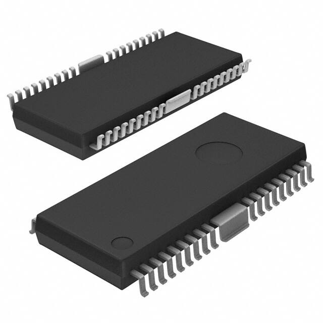
●Package
Max 18.75 (include BURR)
BD6941FM
1 PIN mark
Lot No.
HSOP-M36(Unit : mm)
www.rohm.com
© 2009 ROHM Co., Ltd. All rights reserved.
4/8
2009.06 - Rev.A
�Technical Note
BD6941FM
●Signal Table
Input/Output Truth Table
IN
OUT
MODE
INP
INN
MP
MN
H
H
L
L
BRAKE
H
L
H
L
FORWARD
L
H
L
H
REVERSE
L
L
Open
Open
STANDBY
Output Condition
IN
OUT
PO
INP
INN
MODE
H
H
BRAKE
LOAD
NORMAL
H
L *2
SHORT
H/L
FORWARD/
NORMAL
REVERSE
SHORT
STANDBY
-
H
L/H
L
L
L *2
H
*2 refer to timing chart
●PO Output Timing Chart
normal
over current detection
normal
IOCP
Output current
0
Active
MP/MN
Open
PO
TOFF
TON ≒ 10μsec
TON
TOFF ≒ 290μsec
www.rohm.com
© 2009 ROHM Co., Ltd. All rights reserved.
5/8
2009.06 - Rev.A
�Technical Note
BD6941FM
●I/O Circuit Diagram
1)
INP, INN
2)
Vcc
PO
Vcc
INP
PO
INN
100K
SGND
3)
SGND
MP, MN
Vcc
MP, MN
PGND
●Operating Notes
1) Absolute maximum ratings
Use of the IC in excess of absolute maximum ratings such as the applied voltage or operating temperature range may result
in IC damage. Assumptions should not be made regarding the state of the IC (short mode or open mode) when such damage
is suffered. A physical safety measuresuch as a fuse should be implemented when use of the IC in a special mode where the
absolute maximum ratings may be exceeded is anticipated.
2) GND potential
Ensure a minimum GND pin potential in all operating conditions.
3) Thermal design
Use a thermal design that allows for a sufficient margin in light of the power dissipation (Pd) in actual operating conditions.
4) Pin short and mistake mounting
Use caution when orienting and positioning the IC for mounting on printed circuit boards. Improper mounting may result in
damage to the IC.Shorts between output pins and the power supply and GND pins caused by the presence of a foreign
object may result in damage to the IC. Ensure a minimum GND pin potential in all operating conditions.
5) Actions in strong magnetic field
Keep in mind that the IC may malfunction in strong magnetic fields.
6) Testing on application boards
When testing the IC on an application board, connecting a capacitor to a pin with low impedance subjects the IC to stress.
Always discharge capacitors after each process or step. Always turn the IC's power supply off before connecting it to or
removing it from a jig or fixture during the inspection process. Ground the IC during assembly steps as an antistatic measure,
and use similar caution when transporting or storing the IC.
www.rohm.com
© 2009 ROHM Co., Ltd. All rights reserved.
6/8
2009.06 - Rev.A
�Technical Note
BD6941FM
7) IC terminal input voltage
This monolithic IC contains P+ isolation and P substrate layers between adjacent elements in order to keep them isolated.
P/N junctions are formed at the intersection of these P layers with the N layers of other elements to create a variety of
parasitic elements. For example, when the resistors and transistors are connected to the pins as shown in the following
figure,
The P/N junction functions as a parasitic diode when GND > Pin A for the resistor or GND > Pin B for the transistor(NPN).
Similarly, when GND > Pin B for the transistor (NPN), the parasitic diode described above combines with the N layer of
other adjacent elements to operate as a parasitic NPN transistor.
The formation of parasitic elements as a result of the relationships of the potentials of different pins is an inevitable result of
the IC's architecture. The operation of parasitic elements can cause interference with circuit operation as well as IC
malfunction and damage. For these reasons, it is necessary to use caution so that the IC is not used in a way that will trigger
the operation of parasitic elements, such as by the application of voltages lower than the GND (P substrate) voltage to input
pins.
Transistor (NPN)
(Pin A)
Resistor
B
(Pin B)
C
(Pin B)
E
B
C
N
P
P+
P+
N
N
P
P
P+
N
N
Parasitic elements
GND
P+
N
Parasitic elements or
N
P substrate
(Pin A)
GND
GND
Parasitic elements
or Transistors
Parasitic elements
8) Input terminals
Do not apply the voltage to input pin when the Vcc is not applied. And when the Vcc is applied, the voltage of input pin
must not exceed Vcc. It is feared that output get malfunction, as input voltage is sweeped slowly near the H, L threshold
voltage. Please pay attention to input slew rate.
9) Back electro motive force (BEMF)
There is a possibility that the BEMF is changed by use of the operating condition, environment and the individual
characteristics of motor. Please make sure there is no problem of operating the IC although the BEMF is occurred.
10) The note of pattern design at printed circuit
This IC flows large current between power supply for motor division and GND. So, it is feared that get undesirable result
malfunction, oscillation and so on, as input lines is affected by large output current. Please consider pattern design at
printed circuit doesn’t have common impedance on output large current lines-input lines. Please consider to keep low
impedance of power supply for fear of oscillation from power supply high impedance, also.
11) Rash current
This IC doesn’t have current limit circuit for rash current. Therefore physical security countermeasure, like current limit
resistor is to be given.
12) Thermal shutdown circuit
This IC incorporates a built-in TSD circuit for the protection from thermal destruction. The IC should be used within the
specified power dissipation range. However, in the event that the IC continues to be operated in excess of its power
dissipation limits , the attendant rise in the junction temperature (Tj) will trigger the TSD circuit to turn off all output power
elements. The circuit automatically resets once the junction temperature (Tj) drops. Operation of the TSD circuit presumes
that the IC's absolute maximum ratings have been exceeded. Application designs should never make use of the TSD circuit.
13) Over voltage lock out function
This IC has the function of turning off the output when detecting the over voltage. More than 30V(typ.) triggers this
function. But in the standby mode, this function does not work. Although this IC has over voltage lockout function, the
voltage that exceeds absolute maximum ratings might destroy the IC. Please do not exceed the absolute maximum
ratings.
www.rohm.com
© 2009 ROHM Co., Ltd. All rights reserved.
7/8
2009.06 - Rev.A
�Technical Note
BD6941FM
14)Over current protection
This IC has the function of turning off the output when detecting the over current. More than 2.25A(typ.) triggers this
function. When detecting the over current for 10μsec(typ.), this function turns off the output(output terminals become
Hi-impedance) for 290μsec(typ.). After the period of turning off time (290μsec) , the output current recovers. But if the
over current is still detected, this function will work again.This function is for protecting IC because of the output short etc.
but the continuing detection of over current might cause the extreme heat and damage the IC. It is recommended to
change the IC’s state to standby mode by the application. And please pay attention to the power dissipation.
●Ordering part number
B
D
6
Part No.
9
4
1
F
Part No.
M
-
E
Package
FM : HSOP-M36
2
Packaging and forming specification
E2: Embossed tape and reel
HSOP-M36
18.5±0.1
(MAX 18.75 include BURR)
+6
4 –4
2.77±0.1
0.1 ± 0.05
2.2 ± 0.05
9
Direction
of feed
E2
The direction is the 1pin of product is at the upper left when you hold
( reel on the left hand and you pull out the tape on the right hand
)
18
10
+0.05
0.37 –0.04
1500pcs
19
+0.055
0.27 –0.045
1PIN MARK
0.8
Embossed carrier tape (with dry pack)
Quantity
1.2 ± 0.2
27
0.5 ± 0.15
1
0.85
2.4MAX
28
7.5 ± 0.1
9.9 ± 0.2
36
Tape
0.08 S
0.08
M
1pin
Reel
(Unit : mm)
www.rohm.com
© 2009 ROHM Co., Ltd. All rights reserved.
8/8
Direction of feed
∗ Order quantity needs to be multiple of the minimum quantity.
2009.06 - Rev.A
�Datasheet
Notice
Precaution on using ROHM Products
1.
Our Products are designed and manufactured for application in ordinary electronic equipments (such as AV equipment,
OA equipment, telecommunication equipment, home electronic appliances, amusement equipment, etc.). If you
(Note 1)
, transport
intend to use our Products in devices requiring extremely high reliability (such as medical equipment
equipment, traffic equipment, aircraft/spacecraft, nuclear power controllers, fuel controllers, car equipment including car
accessories, safety devices, etc.) and whose malfunction or failure may cause loss of human life, bodily injury or
serious damage to property (“Specific Applications”), please consult with the ROHM sales representative in advance.
Unless otherwise agreed in writing by ROHM in advance, ROHM shall not be in any way responsible or liable for any
damages, expenses or losses incurred by you or third parties arising from the use of any ROHM’s Products for Specific
Applications.
(Note1) Medical Equipment Classification of the Specific Applications
JAPAN
USA
EU
CHINA
CLASSⅢ
CLASSⅡb
CLASSⅢ
CLASSⅢ
CLASSⅣ
CLASSⅢ
2.
ROHM designs and manufactures its Products subject to strict quality control system. However, semiconductor
products can fail or malfunction at a certain rate. Please be sure to implement, at your own responsibilities, adequate
safety measures including but not limited to fail-safe design against the physical injury, damage to any property, which
a failure or malfunction of our Products may cause. The following are examples of safety measures:
[a] Installation of protection circuits or other protective devices to improve system safety
[b] Installation of redundant circuits to reduce the impact of single or multiple circuit failure
3.
Our Products are designed and manufactured for use under standard conditions and not under any special or
extraordinary environments or conditions, as exemplified below. Accordingly, ROHM shall not be in any way
responsible or liable for any damages, expenses or losses arising from the use of any ROHM’s Products under any
special or extraordinary environments or conditions. If you intend to use our Products under any special or
extraordinary environments or conditions (as exemplified below), your independent verification and confirmation of
product performance, reliability, etc, prior to use, must be necessary:
[a] Use of our Products in any types of liquid, including water, oils, chemicals, and organic solvents
[b] Use of our Products outdoors or in places where the Products are exposed to direct sunlight or dust
[c] Use of our Products in places where the Products are exposed to sea wind or corrosive gases, including Cl2,
H2S, NH3, SO2, and NO2
[d] Use of our Products in places where the Products are exposed to static electricity or electromagnetic waves
[e] Use of our Products in proximity to heat-producing components, plastic cords, or other flammable items
[f] Sealing or coating our Products with resin or other coating materials
[g] Use of our Products without cleaning residue of flux (even if you use no-clean type fluxes, cleaning residue of
flux is recommended); or Washing our Products by using water or water-soluble cleaning agents for cleaning
residue after soldering
[h] Use of the Products in places subject to dew condensation
4.
The Products are not subject to radiation-proof design.
5.
Please verify and confirm characteristics of the final or mounted products in using the Products.
6.
In particular, if a transient load (a large amount of load applied in a short period of time, such as pulse. is applied,
confirmation of performance characteristics after on-board mounting is strongly recommended. Avoid applying power
exceeding normal rated power; exceeding the power rating under steady-state loading condition may negatively affect
product performance and reliability.
7.
De-rate Power Dissipation (Pd) depending on Ambient temperature (Ta). When used in sealed area, confirm the actual
ambient temperature.
8.
Confirm that operation temperature is within the specified range described in the product specification.
9.
ROHM shall not be in any way responsible or liable for failure induced under deviant condition from what is defined in
this document.
Precaution for Mounting / Circuit board design
1.
When a highly active halogenous (chlorine, bromine, etc.) flux is used, the residue of flux may negatively affect product
performance and reliability.
2.
In principle, the reflow soldering method must be used; if flow soldering method is preferred, please consult with the
ROHM representative in advance.
For details, please refer to ROHM Mounting specification
Notice - GE
© 2014 ROHM Co., Ltd. All rights reserved.
Rev.002
�Datasheet
Precautions Regarding Application Examples and External Circuits
1.
If change is made to the constant of an external circuit, please allow a sufficient margin considering variations of the
characteristics of the Products and external components, including transient characteristics, as well as static
characteristics.
2.
You agree that application notes, reference designs, and associated data and information contained in this document
are presented only as guidance for Products use. Therefore, in case you use such information, you are solely
responsible for it and you must exercise your own independent verification and judgment in the use of such information
contained in this document. ROHM shall not be in any way responsible or liable for any damages, expenses or losses
incurred by you or third parties arising from the use of such information.
Precaution for Electrostatic
This Product is electrostatic sensitive product, which may be damaged due to electrostatic discharge. Please take proper
caution in your manufacturing process and storage so that voltage exceeding the Products maximum rating will not be
applied to Products. Please take special care under dry condition (e.g. Grounding of human body / equipment / solder iron,
isolation from charged objects, setting of Ionizer, friction prevention and temperature / humidity control).
Precaution for Storage / Transportation
1.
Product performance and soldered connections may deteriorate if the Products are stored in the places where:
[a] the Products are exposed to sea winds or corrosive gases, including Cl2, H2S, NH3, SO2, and NO2
[b] the temperature or humidity exceeds those recommended by ROHM
[c] the Products are exposed to direct sunshine or condensation
[d] the Products are exposed to high Electrostatic
2.
Even under ROHM recommended storage condition, solderability of products out of recommended storage time period
may be degraded. It is strongly recommended to confirm solderability before using Products of which storage time is
exceeding the recommended storage time period.
3.
Store / transport cartons in the correct direction, which is indicated on a carton with a symbol. Otherwise bent leads
may occur due to excessive stress applied when dropping of a carton.
4.
Use Products within the specified time after opening a humidity barrier bag. Baking is required before using Products of
which storage time is exceeding the recommended storage time period.
Precaution for Product Label
QR code printed on ROHM Products label is for ROHM’s internal use only.
Precaution for Disposition
When disposing Products please dispose them properly using an authorized industry waste company.
Precaution for Foreign Exchange and Foreign Trade act
Since our Products might fall under controlled goods prescribed by the applicable foreign exchange and foreign trade act,
please consult with ROHM representative in case of export.
Precaution Regarding Intellectual Property Rights
1.
All information and data including but not limited to application example contained in this document is for reference
only. ROHM does not warrant that foregoing information or data will not infringe any intellectual property rights or any
other rights of any third party regarding such information or data. ROHM shall not be in any way responsible or liable
for infringement of any intellectual property rights or other damages arising from use of such information or data.:
2.
No license, expressly or implied, is granted hereby under any intellectual property rights or other rights of ROHM or any
third parties with respect to the information contained in this document.
Other Precaution
1.
This document may not be reprinted or reproduced, in whole or in part, without prior written consent of ROHM.
2.
The Products may not be disassembled, converted, modified, reproduced or otherwise changed without prior written
consent of ROHM.
3.
In no event shall you use in any way whatsoever the Products and the related technical information contained in the
Products or this document for any military purposes, including but not limited to, the development of mass-destruction
weapons.
4.
The proper names of companies or products described in this document are trademarks or registered trademarks of
ROHM, its affiliated companies or third parties.
Notice - GE
© 2014 ROHM Co., Ltd. All rights reserved.
Rev.002
�Datasheet
General Precaution
1. Before you use our Pro ducts, you are requested to care fully read this document and fully understand its contents.
ROHM shall n ot be in an y way responsible or liabl e for fa ilure, malfunction or acci dent arising from the use of a ny
ROHM’s Products against warning, caution or note contained in this document.
2. All information contained in this docume nt is current as of the issuing date and subj ect to change without any prior
notice. Before purchasing or using ROHM’s Products, please confirm the la test information with a ROHM sale s
representative.
3.
The information contained in this doc ument is provi ded on an “as is” basis and ROHM does not warrant that all
information contained in this document is accurate an d/or error-free. ROHM shall not be in an y way responsible or
liable for an y damages, expenses or losses incurred b y you or third parties resulting from inaccur acy or errors of or
concerning such information.
Notice – WE
© 2014 ROHM Co., Ltd. All rights reserved.
Rev.001
�


 工商网监
湘ICP备2023018690号
工商网监
湘ICP备2023018690号
