Datasheet
Single-chip Type with Built-in FET Switching Regulators
Simple Step-down
Switching Regulators
with Built-in Power MOSFET
BD9G101G
General Description
Key Specifications
The BD9G101G is high voltage input 42V step-down
switching regulator with integrated internal Power
MOSFET.
It provides maximum 0.5A output with small SSOP6
package.
It is allowing the use of small inductor by high frequency
operation of 1.5MHz. Also, it is implemented to downsize
by incorporation of phase compensation parts with
current mode.
◼ Input Voltage
6V to 42 V
◼ Reference Voltage Precision (Ta=25°C)
±1.5 %
(Ta=-25°C to 105°C) ±2.0 %
◼ Max Output Current
0.5 A (Max)
◼ Operating Temperature
-40°C to +105°C
◼ Max Junction Temperature
150°C
Features
Packages
W(Typ) x D(Typ) x H(Max)
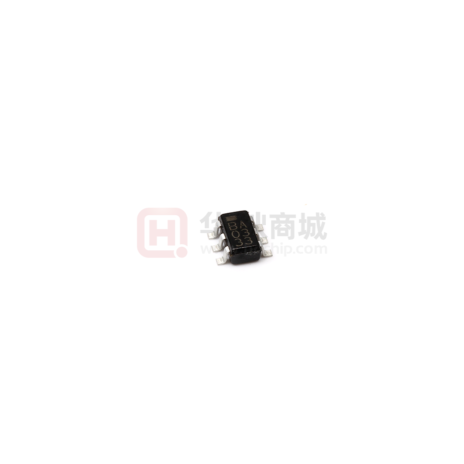
SSOP6
2.90mm x 2.80mm x 1.25mm
High and Wide Input Voltage Range (VCC=6V to 42V)
45V/800mΩ Internal Power Nch-FET
1.5MHz Fixed Operating High Frequency
Built-in Reference Voltage 0.75V±1.5% circuit
Built-in Phase Compensation circuit
Internal Over Current protection, Under Voltage Lock
Out, Thermal shutdown
◼ Stand-by function (Ist=0µA)
◼ Small package SSOP6
◼
◼
◼
◼
◼
◼
SSOP6
Applications
◼
◼
◼
Industrial distributed power applications
Battery powered equipment
OA instruments
Typical Application Circuits
15000pF
5V/0.5A
L1:6.8μH
BST
LX
D1
GND
VCC
C2:10μF/10V
VCC
C1:4.7μF/50V
FB
EN
ON/OFF control
680Ω
0.1μF
3.9kΩ
Figure 1. Typical Application Circuit
〇Product structure : Silicon integrated circuit
www.rohm.com
© 2012 ROHM Co., Ltd. All rights reserved.
TSZ22111 • 14 • 001
〇This product has no designed protection against radioactive rays
1/25
TSZ02201-0Q1Q0AJ00150-1-2
03.Dec.2021 Rev.009
�BD9G101G
Pin Configuration
BST
1
6
LX
GND
2
5
VCC
FB
3
4
EN
Figure 2. Pin Configuration (TOP VIEW)
Pin Description
Pin No.
Pin Name
Description
1
BST
The pin is power supply for floating Power Nch-FET driver. Connected
15000pF between this pin and LX pin for bootstrap operation.
2
GND
Ground.
3
FB
Voltage feedback pin. This pin is error-amplifier input, the DCDC is set 0.75V
at this pin with feed-back operation.
4
EN
ON/OFF pin. The IC is start-up to apply 2.0V or over.
This pin has pull-down resister 550kΩ, the IC is shutdown to open or apply
0.8V or under.
5
VCC
Input supply. It should be connected as near as possible to the bypass
capacitor. It should be increased impedance by thick PCB pattern.
6
LX
Power Nch-FET switching node pin. It should be connected as near as
possible to the schottky barrier diode, and inductor.
Block Diagram
ON/OFF
EN
VCC
TSD
UVLO
Reference
REG
VREF
Current Sense
AMP
shutdown
FB
0.75V
+
+
Error
AMP
OCP
Σ
Current
Comparator
R Q
+
S
BST
800mΩ
VOUT
LX
Soft
Start
Oscillator
1.5MHz
GND
Figure 3. Block Diagram
www.rohm.com
© 2012 ROHM Co., Ltd. All rights reserved.
TSZ22111 • 15 • 001
2/25
TSZ02201-0Q1Q0AJ00150-1-2
03.Dec.2021 Rev.009
�BD9G101G
Description of Blocks
1.
Reference
This block generates reference voltage. It starts operation by applying EN 2.0V or more.
It provides reference voltage and current to error-amp, oscillator, and etc.
2.
REG
This is a gate drive voltage generator and 4.2V regulator for internal circuit power supply.
3.
OSC
It is generated rectangular wave of 1.5MHz with operation frequency of normal time.
To protect over current from output shorted to GND, the frequency is changed depending on FB voltage by the Frequency
fold-back function.
4.
Soft Start
This block does Soft Start to the output voltage of DC/DC converter, and prevents in-rush current during Start-up.
Soft Start Time depend on application start-condition because the Frequency fold-back function is built-in. The Frequency
fold-back function changes frequency by FB voltage.
5.
ERROR AMP
This is an error-amplifier what detects output signal, and outputs PWM control signal.
Internal reference voltage is set to 0.75V. Also, the BD9G101G has internal phase compensated element between
ERROR AMPs’ input and output.
6.
Current Comparator
This is a comparator that outputs PWM signal from current feed-back signal and error-amplifier output for current-mode.
7.
Nch-FET SW
This is an 45V/800mΩ Power Nch-FET SW that converts inductor current of DC/DC converter.
8.
UVLO
This is a low voltage error prevention circuit.
This prevents internal circuit error during increase of power supply voltage and during decline of power supply voltage.
It monitors VCC pin voltage, and when VCC voltage becomes 5.4V and below, it turns OFF DC/DC converter output,
and Soft Start circuit resets.
Now this threshold has hysteresis of 200mV.
9.
EN
When a Voltage of 2.0V or more is applied, it turns ON. at open or 0.8V or under applied, it turns OFF.
550kΩ (Typ) Pull-down Resistance is contained in the Pin.
10. OCP
This is Over Current protection.
It monitors current of high-side Nch-FET. If the current is 1.2A (Typ) or more, this function reduce duty by pulse-bypulse and restrict the input current.
11.TSD
This is circuit for preventing malfunction at high Temperature.
When it detects an abnormal temperature Tj=175°C, it turns OFF DC/DC Converter Output. The protection circuit has
Hysteresis (25°C). It prevents malfunction by changing near threshold.
www.rohm.com
© 2012 ROHM Co., Ltd. All rights reserved.
TSZ22111 • 15 • 001
3/25
TSZ02201-0Q1Q0AJ00150-1-2
03.Dec.2021 Rev.009
�BD9G101G
Absolute Maximum Ratings
Item
Symbol
Ratings
Unit
VCC to GND
VCC
45
V
BST to GND
VBST
50
V
Maximum rating current
Imax
1.0
A
BST to LX
∆VBST
7
V
EN to GND
VEN
45
V
LX to GND
VLX
45
V
FB to GND
VFB
7
V
Power Dissipation
Pd
0.675(*1)
W
Operating Temperature
Topr
-40 to +105
°C
Storage Temperature
Tstg
-55 to +150
°C
Tjmax
150(*2)
°C
Junction Temperature
(*1) During mounting of 70mm x 70mm x 1.6mmt 1layer board. Reduce by 5.4mW for every 1°C increase. (25°C or more)
(*2) This is circuit for preventing malfunction at high Temperature.
When it detects an abnormal temperature Tj=175°C, it turns OFF DC/DC Converter Output.
The protection circuit has Hysteresis (25°C). It prevents malfunction by changing near threshold
Electrical Characteristics (Unless otherwise specified Ta=25°C, VCC=24V, VOUT=5V, EN=3V)
Parameter
Symbol
Limit
Min
Typ
Max
Unit
Condition
Circuit Current
Stand-by Current
Ist
-
0
5
µA
VEN=0V
Operating Current
Icc
-
0.7
1.2
mA
FB=1.2V
Vuv
5.1
5.4
5.7
V
Vuvhy
-
200
300
mV
Switching Frequency
Fosc
1.3
1.5
1.7
MHz
Max Duty Cycle
Dmax
85
-
-
%
VFBN
0.739
0.750
0.761
V
VFBA
IFB
Tsoft
0.735
-100
1.2
0.750
0
4.0
0.765
100
-
V
nA
ms
GCS
-
3
-
A/V
High-side Nch-FET ON Resistance
RonH
-
800
-
mΩ
Min ON Time
Tmin
-
100
-
ns
OCP Detect Current
Iocp
0.85
1.2
-
A
VENON
2.0
-
VCC
V
OFF VENOFF
IEN
-0.3
2.7
5.5
0.8
11
V
µA
Under Voltage Lock Out (UVLO)
Detect Threshold Voltage
Hysteresis width
Oscillator
Error AMP
FB Pin Threshold Voltage
FB Pin Input Current
Soft-Start Time
Ta=25°C
Ta=-25°C to 105°C
VFB=2.0V
Current Comparator
Trans-conductance
Output
CTL
EN Thresohold Voltage
EN Input Current
www.rohm.com
© 2012 ROHM Co., Ltd. All rights reserved.
TSZ22111 • 15 • 001
ON
4/25
VEN=3V
TSZ02201-0Q1Q0AJ00150-1-2
03.Dec.2021 Rev.009
�BD9G101G
Operating Ratings
Item
Symbol
Input Voltage
Output Voltage
Ratings
Min
Typ
Max
VCC
6
-
42
VOUT
1.0(*3)
-
Output Current
IOUT
(*3) Restricted by Min ON Time typ 100ns.
(*4) Restricted by Max duty, RonH and BST-UVLO.
VCC x
-
0.7(*4)
500
Unit
V
V
mA
Output voltage range and Output voltage setting
BD9G101G is limited the range of use by Max duty (min85%), Min ON Time (Typ 100ns), high-side Nch-FET ON resistance
(RonH) and low voltage protect (BST-UVLO) for drive voltage of high-side Nch-FET between BST and LX.
1. BST-UVLO
It is the function that secure gate voltage of Nch-FET and prevent malfunction of the IC. If the voltage between BST and LX is
lower than 1.5V, Nch-FET is turned off and there is new pass to charge voltage VCC to BST. BST voltage is charged by VCC.
If the voltage between BST and LX is upper than 1.8V, BST-UVLO is released.
The condition that BST-UVLO is working property is
VCC > (BST-UVLO + Vf) + VOUT.
Therefore, maximum output voltage is restricted VCC -3V.
BST charging current (normal mode)
4.2V
BST
BST charging current
(BST-UVLO mode)
BSTUVLO
VCC
Nch-FET OFF
(BST-UVLO mode)
LX
Figure 4. BST-UVLO equivalent circuit
*When operation can be considered by VCC-VOUT Output capacitor or Catch diode
-> Inductor -> Output capacitor. Therefore, the distance between the output capacitor and the catch diode, or the distance
between the output capacitor and the bypass input capacitor on the GND pattern should be as short as possible.
The input bypass capacitor, the catch diode and the inductor should be located as close to the IC as possible. Please keep
GND line on the top layer to avoid GND level fluctuation caused by external connection.
www.rohm.com
© 2012 ROHM Co., Ltd. All rights reserved.
TSZ22111 • 15 • 001
18/25
TSZ02201-0Q1Q0AJ00150-1-2
03.Dec.2021 Rev.009
�BD9G101G
Power Dissipation
Figure 48 shows reducing characteristics of power dissipation measured with mount 70mm x 70mm x 1.6mmt, 1layer PCB.
Junction temperature must be designed not to exceed 150°C and it should have margin design.
In actual use, it has difference of power dissipation and temperature increase by another heat source. Please examine it
enough.
Power Dissipation : Pd (W)
1.5
1
675mW
0.5
0
0
25
50
75
100
125
Ambient Temperature: Ta(°C)
150
Figure 48. Power Dissipation (70mm x 70mm x 1.6mmt 1layer PCB)
Power Dissipation Estimate
The following formulas show how to estimate the device power dissipation under continuous mode operations. Do not use
these formulas, if the device is working in the discontinuous conduction mode.
The device power dissipation includes:
1) Conduction loss : Pcon = IOUT2 x RonH x VOUT/VCC
2) Switching loss : Psw = 2.5 x 10⁻⁹ x VCC x IOUT × fsw
3) Gate charge loss : Pgc = 4.88 x 10⁻⁹ x fsw
4) Current loss at non switching : Pq = 0.8 x 10⁻³ x VCC
Where:
IOUT is the output current (A), RonH is the on-resistance of the high-side Nch-FET(Ω), VOUT is the output voltage (V).
VCC is the input voltage (V), fsw is the switching frequency (Hz).
Therefore
Power dissipation of IC (Pd) is the sum of above dissipation.
Pd = Pcon + Psw + Pgc + Pq
The junction temperature is as follows.
Tj =Ta + θja x Pd
Where:
Ta is the ambient temperature (°C)
Tj is the junction temperature (°C), θja is the thermal resistance of the package (°C)
Please design thermal design with enough margin so that the junction temperature is not beyond maximum Tj_max=150°C.
www.rohm.com
© 2012 ROHM Co., Ltd. All rights reserved.
TSZ22111 • 15 • 001
19/25
TSZ02201-0Q1Q0AJ00150-1-2
03.Dec.2021 Rev.009
�BD9G101G
I/O equivalent circuit
Pin.
No
Pin
Name
6
LX
2
GND
1
BST
5
VCC
Pin Equivalent Circuit
Pin.
No
Pin
Name
4
EN
Pin Equivalent Circuit
BST
VCC
EN
LX
GND
GND
FB
3
FB
GND
Figure 49. I/O equivalent circuit
www.rohm.com
© 2012 ROHM Co., Ltd. All rights reserved.
TSZ22111 • 15 • 001
20/25
TSZ02201-0Q1Q0AJ00150-1-2
03.Dec.2021 Rev.009
�BD9G101G
Operational Notes
1.
Reverse Connection of Power Supply
Connecting the power supply in reverse polarity can damage the IC. Take precautions against reverse polarity when
connecting the power supply, such as mounting an external diode between the power supply and the IC’s power supply
pins.
2.
Power Supply Lines
Design the PCB layout pattern to provide low impedance supply lines. Furthermore, connect a capacitor to ground at
all power supply pins. Consider the effect of temperature and aging on the capacitance value when using electrolytic
capacitors.
3.
Ground Voltage
Ensure that no pins are at a voltage below that of the ground pin at any time, even during transient condition.
4.
Ground Wiring Pattern
When using both small-signal and large-current ground traces, the two ground traces should be routed separately but
connected to a single ground at the reference point of the application board to avoid fluctuations in the small-signal
ground caused by large currents. Also ensure that the ground traces of external components do not cause variations
on the ground voltage. The ground lines must be as short and thick as possible to reduce line impedance.
5.
Recommended Operating Conditions
The function and operation of the IC are guaranteed within the range specified by the recommended operating
conditions. The characteristic values are guaranteed only under the conditions of each item specified by the electrical
characteristics.
6.
Inrush Current
When power is first supplied to the IC, it is possible that the internal logic may be unstable and inrush current may flow
instantaneously due to the internal powering sequence and delays, especially if the IC has more than one power supply.
Therefore, give special consideration to power coupling capacitance, power wiring, width of ground wiring, and routing
of connections.
7.
Testing on Application Boards
When testing the IC on an application board, connecting a capacitor directly to a low-impedance output pin may subject
the IC to stress. Always discharge capacitors completely after each process or step. The IC’s power supply should
always be turned off completely before connecting or removing it from the test setup during the inspection process. To
prevent damage from static discharge, ground the IC during assembly and use similar precautions during transport and
storage.
8.
Inter-pin Short and Mounting Errors
Ensure that the direction and position are correct when mounting the IC on the PCB. Incorrect mounting may result in
damaging the IC. Avoid nearby pins being shorted to each other especially to ground, power supply and output pin.
Inter-pin shorts could be due to many reasons such as metal particles, water droplets (in very humid environment) and
unintentional solder bridge deposited in between pins during assembly to name a few.
9.
Unused Input Pins
Input pins of an IC are often connected to the gate of a MOS transistor. The gate has extremely high impedance and
extremely low capacitance. If left unconnected, the electric field from the outside can easily charge it. The small charge
acquired in this way is enough to produce a significant effect on the conduction through the transistor and cause
unexpected operation of the IC. So unless otherwise specified, unused input pins should be connected to the power
supply or ground line.
www.rohm.com
© 2012 ROHM Co., Ltd. All rights reserved.
TSZ22111 • 15 • 001
21/25
TSZ02201-0Q1Q0AJ00150-1-2
03.Dec.2021 Rev.009
�BD9G101G
Operational Notes – continued
10. Regarding the Input Pin of the IC
This monolithic IC contains P+ isolation and P substrate layers between adjacent elements in order to keep them
isolated. P-N junctions are formed at the intersection of the P layers with the N layers of other elements, creating a
parasitic diode or transistor. For example (refer to figure below):
When GND > Pin A and GND > Pin B, the P-N junction operates as a parasitic diode.
When GND > Pin B, the P-N junction operates as a parasitic transistor.
Parasitic diodes inevitably occur in the structure of the IC. The operation of parasitic diodes can result in mutual
interference among circuits, operational faults, or physical damage. Therefore, conditions that cause these diodes to
operate, such as applying a voltage lower than the GND voltage to an input pin (and thus to the P substrate) should be
avoided.
Resistor
Transistor (NPN)
Pin A
Pin B
C
E
Pin A
N
P+
P
N
N
P+
N
Pin B
B
Parasitic
Elements
N
P+
N P
N
P+
B
N
C
E
Parasitic
Elements
P Substrate
P Substrate
GND
GND
Parasitic
Elements
GND
Parasitic
Elements
GND
N Region
close-by
Figure50. Example of monolithic IC structure
11. Ceramic Capacitor
When using a ceramic capacitor, determine a capacitance value considering the change of capacitance with
temperature and the decrease in nominal capacitance due to DC bias and others.
12. Thermal Shutdown Circuit(TSD)
This IC has a built-in thermal shutdown circuit that prevents heat damage to the IC. Normal operation should always
be within the IC’s maximum junction temperature rating. If however the rating is exceeded for a continued period, the
junction temperature (Tj) will rise which will activate the TSD circuit that will turn OFF power output pins. When the Tj
falls below the TSD threshold, the circuits are automatically restored to normal operation.
Note that the TSD circuit operates in a situation that exceeds the absolute maximum ratings and therefore, under no
circumstances, should the TSD circuit be used in a set design or for any purpose other than protecting the IC from heat
damage.
13.
Over Current Protection Circuit (OCP)
This IC incorporates an integrated overcurrent protection circuit that is activated when the load is shorted. This
protection circuit is effective in preventing damage due to sudden and unexpected incidents. However, the IC should
not be used in applications characterized by continuous operation or transitioning of the protection circuit.
www.rohm.com
© 2012 ROHM Co., Ltd. All rights reserved.
TSZ22111 • 15 • 001
22/25
TSZ02201-0Q1Q0AJ00150-1-2
03.Dec.2021 Rev.009
�BD9G101G
Ordering part number
B
D
9
G
1
Part Number
0
1
G
Package
G: SSOP6
-
TR
Packaging and forming specification
TR: Embossed tape and reel
Marking Diagram
SSOP6(TOP VIEW)
B
A
Part Number Marking
Pin 1 Mark
LOT Number
www.rohm.com
© 2012 ROHM Co., Ltd. All rights reserved.
TSZ22111 • 15 • 001
23/25
TSZ02201-0Q1Q0AJ00150-1-2
03.Dec.2021 Rev.009
�BD9G101G
Physical Dimension and Packing Information
Package Name
www.rohm.com
© 2012 ROHM Co., Ltd. All rights reserved.
TSZ22111 • 15 • 001
SSOP6
24/25
TSZ02201-0Q1Q0AJ00150-1-2
03.Dec.2021 Rev.009
�BD9G101G
Revision History
Date
Revision
Changes
21.Aug.2012
001
04.Feb.2013
002
22.Mar.2013
04.Mar.2014
13.Jan.2015
16.Feb.2015
26.Jun.2017
003
004
005
006
007
11.Dec.2018
008
03.Dec.2021
009
New Release
P5~6: Adding of output voltage range
P1, 10, 13: Change of typical application circuit
P12, 15: Change of typical performance characteristic
P16: Added description of input capacitor
P10, 13: Correction of application parts
P19: Correction of erroneous power dissipation estimate
P23: Correction of ordering part number format
P17: Correction of erroneous feed-forward capacitor formula
P1: Deletion of car application in use application
P11, 14: Correction of characteristics in typical application
Review sentences over all pages
P1 Changed the text on the lower-right of the footer.
P3 1. Reference: Partly changed the description.
P3 4. Soft Start: Partly changed the description: "DC/DC comparator"->"DC/DC convertor".
P3 5. ERROR AMP: Partly changed the description.
P3 10. OCP: Partly changed the description: "the over current"->"the input current"
P4 Partly changed the description int the first foot note of Absolute Maximum Ratings:
"70x70x1.6t mm"->"70mm x 70mm x 1.6mmt"
P6 1.2 Feed-forward capacitor Csp: Partly changed the description.
P7 Changed the description of Figure 7.
P7 Start-up Characteristics: Partly changed the description.
P10 Figure 20 Changed the format of the graph.
P12 Figure 28, Figure 29 Changed the label on VOUT: "VOUT:offset 5V"-> "VOUT(AC)"
P13 Figure 33 Changed the format of the graph.
P15 Figure 41, Figure 42 Fixed the label of VOUT:"VOUT:offset 12V"->" VOUT(AC)"
P16 (1)Inductor: Fixed the model name of the recommended inductor (TOKO DE4518C
Series -> TOKO DEM4518C Series)
P18 Cautions on PCB Layout: Partly changed the description.
www.rohm.com
© 2012 ROHM Co., Ltd. All rights reserved.
TSZ22111 • 15 • 001
25/25
TSZ02201-0Q1Q0AJ00150-1-2
03.Dec.2021 Rev.009
�Notice
Precaution on using ROHM Products
1.
Our Products are designed and manufactured for application in ordinary electronic equipment (such as AV equipment,
OA equipment, telecommunication equipment, home electronic appliances, amusement equipment, etc.). If you
intend to use our Products in devices requiring extremely high reliability (such as medical equipment (Note 1), transport
equipment, traffic equipment, aircraft/spacecraft, nuclear power controllers, fuel controllers, car equipment including car
accessories, safety devices, etc.) and whose malfunction or failure may cause loss of human life, bodily injury or
serious damage to property (“Specific Applications”), please consult with the ROHM sales representative in advance.
Unless otherwise agreed in writing by ROHM in advance, ROHM shall not be in any way responsible or liable for any
damages, expenses or losses incurred by you or third parties arising from the use of any ROHM’s Products for Specific
Applications.
(Note1) Medical Equipment Classification of the Specific Applications
JAPAN
USA
EU
CHINA
CLASSⅢ
CLASSⅡb
CLASSⅢ
CLASSⅢ
CLASSⅣ
CLASSⅢ
2.
ROHM designs and manufactures its Products subject to strict quality control system. However, semiconductor
products can fail or malfunction at a certain rate. Please be sure to implement, at your own responsibilities, adequate
safety measures including but not limited to fail-safe design against the physical injury, damage to any property, which
a failure or malfunction of our Products may cause. The following are examples of safety measures:
[a] Installation of protection circuits or other protective devices to improve system safety
[b] Installation of redundant circuits to reduce the impact of single or multiple circuit failure
3.
Our Products are designed and manufactured for use under standard conditions and not under any special or
extraordinary environments or conditions, as exemplified below. Accordingly, ROHM shall not be in any way
responsible or liable for any damages, expenses or losses arising from the use of any ROHM’s Products under any
special or extraordinary environments or conditions. If you intend to use our Products under any special or
extraordinary environments or conditions (as exemplified below), your independent verification and confirmation of
product performance, reliability, etc, prior to use, must be necessary:
[a] Use of our Products in any types of liquid, including water, oils, chemicals, and organic solvents
[b] Use of our Products outdoors or in places where the Products are exposed to direct sunlight or dust
[c] Use of our Products in places where the Products are exposed to sea wind or corrosive gases, including Cl2,
H2S, NH3, SO2, and NO2
[d] Use of our Products in places where the Products are exposed to static electricity or electromagnetic waves
[e] Use of our Products in proximity to heat-producing components, plastic cords, or other flammable items
[f] Sealing or coating our Products with resin or other coating materials
[g] Use of our Products without cleaning residue of flux (Exclude cases where no-clean type fluxes is used.
However, recommend sufficiently about the residue.) ; or Washing our Products by using water or water-soluble
cleaning agents for cleaning residue after soldering
[h] Use of the Products in places subject to dew condensation
4.
The Products are not subject to radiation-proof design.
5.
Please verify and confirm characteristics of the final or mounted products in using the Products.
6.
In particular, if a transient load (a large amount of load applied in a short period of time, such as pulse, is applied,
confirmation of performance characteristics after on-board mounting is strongly recommended. Avoid applying power
exceeding normal rated power; exceeding the power rating under steady-state loading condition may negatively affect
product performance and reliability.
7.
De-rate Power Dissipation depending on ambient temperature. When used in sealed area, confirm that it is the use in
the range that does not exceed the maximum junction temperature.
8.
Confirm that operation temperature is within the specified range described in the product specification.
9.
ROHM shall not be in any way responsible or liable for failure induced under deviant condition from what is defined in
this document.
Precaution for Mounting / Circuit board design
1.
When a highly active halogenous (chlorine, bromine, etc.) flux is used, the residue of flux may negatively affect product
performance and reliability.
2.
In principle, the reflow soldering method must be used on a surface-mount products, the flow soldering method must
be used on a through hole mount products. If the flow soldering method is preferred on a surface-mount products,
please consult with the ROHM representative in advance.
For details, please refer to ROHM Mounting specification
Notice-PGA-E
© 2015 ROHM Co., Ltd. All rights reserved.
Rev.004
�Precautions Regarding Application Examples and External Circuits
1.
If change is made to the constant of an external circuit, please allow a sufficient margin considering variations of the
characteristics of the Products and external components, including transient characteristics, as well as static
characteristics.
2.
You agree that application notes, reference designs, and associated data and information contained in this document
are presented only as guidance for Products use. Therefore, in case you use such information, you are solely
responsible for it and you must exercise your own independent verification and judgment in the use of such information
contained in this document. ROHM shall not be in any way responsible or liable for any damages, expenses or losses
incurred by you or third parties arising from the use of such information.
Precaution for Electrostatic
This Product is electrostatic sensitive product, which may be damaged due to electrostatic discharge. Please take proper
caution in your manufacturing process and storage so that voltage exceeding the Products maximum rating will not be
applied to Products. Please take special care under dry condition (e.g. Grounding of human body / equipment / solder iron,
isolation from charged objects, setting of Ionizer, friction prevention and temperature / humidity control).
Precaution for Storage / Transportation
1.
Product performance and soldered connections may deteriorate if the Products are stored in the places where:
[a] the Products are exposed to sea winds or corrosive gases, including Cl 2, H2S, NH3, SO2, and NO2
[b] the temperature or humidity exceeds those recommended by ROHM
[c] the Products are exposed to direct sunshine or condensation
[d] the Products are exposed to high Electrostatic
2.
Even under ROHM recommended storage condition, solderability of products out of recommended storage time period
may be degraded. It is strongly recommended to confirm solderability before using Products of which storage time is
exceeding the recommended storage time period.
3.
Store / transport cartons in the correct direction, which is indicated on a carton with a symbol. Otherwise bent leads
may occur due to excessive stress applied when dropping of a carton.
4.
Use Products within the specified time after opening a humidity barrier bag. Baking is required before using Products of
which storage time is exceeding the recommended storage time period.
Precaution for Product Label
A two-dimensional barcode printed on ROHM Products label is for ROHM’s internal use only.
Precaution for Disposition
When disposing Products please dispose them properly using an authorized industry waste company.
Precaution for Foreign Exchange and Foreign Trade act
Since concerned goods might be fallen under listed items of export control prescribed by Foreign exchange and Foreign
trade act, please consult with ROHM in case of export.
Precaution Regarding Intellectual Property Rights
1.
All information and data including but not limited to application example contained in this document is for reference
only. ROHM does not warrant that foregoing information or data will not infringe any intellectual property rights or any
other rights of any third party regarding such information or data.
2.
ROHM shall not have any obligations where the claims, actions or demands arising from the combination of the
Products with other articles such as components, circuits, systems or external equipment (including software).
3.
No license, expressly or implied, is granted hereby under any intellectual property rights or other rights of ROHM or any
third parties with respect to the Products or the information contained in this document. Provided, however, that ROHM
will not assert its intellectual property rights or other rights against you or your customers to the extent necessary to
manufacture or sell products containing the Products, subject to the terms and conditions herein.
Other Precaution
1.
This document may not be reprinted or reproduced, in whole or in part, without prior written consent of ROHM.
2.
The Products may not be disassembled, converted, modified, reproduced or otherwise changed without prior written
consent of ROHM.
3.
In no event shall you use in any way whatsoever the Products and the related technical information contained in the
Products or this document for any military purposes, including but not limited to, the development of mass-destruction
weapons.
4.
The proper names of companies or products described in this document are trademarks or registered trademarks of
ROHM, its affiliated companies or third parties.
Notice-PGA-E
© 2015 ROHM Co., Ltd. All rights reserved.
Rev.004
�Datasheet
General Precaution
1. Before you use our Products, you are requested to carefully read this document and fully understand its contents.
ROHM shall not be in any way responsible or liable for failure, malfunction or accident arising from the use of any
ROHM’s Products against warning, caution or note contained in this document.
2. All information contained in this document is current as of the issuing date and subject to change without any prior
notice. Before purchasing or using ROHM’s Products, please confirm the latest information with a ROHM sales
representative.
3.
The information contained in this document is provided on an “as is” basis and ROHM does not warrant that all
information contained in this document is accurate and/or error-free. ROHM shall not be in any way responsible or
liable for an y damages, expenses or losses incurred b y you or third parties resulting from inaccuracy or errors of or
concerning such information.
Notice – WE
© 2015 ROHM Co., Ltd. All rights reserved.
Rev.001
�


 工商网监
湘ICP备2023018690号
工商网监
湘ICP备2023018690号
