Dear customer
LAPIS Semiconductor Co., Ltd. ("LAPIS Semiconductor"), on the 1st day of October,
2020, implemented the incorporation-type company split (shinsetsu-bunkatsu) in which
LAPIS established a new company, LAPIS Technology Co., Ltd. (“LAPIS
Technology”) and LAPIS Technology succeeded LAPIS Semiconductor’s LSI business.
Therefore, all references to "LAPIS Semiconductor Co., Ltd.", "LAPIS Semiconductor"
and/or "LAPIS" in this document shall be replaced with "LAPIS Technology Co., Ltd."
Furthermore, there are no changes to the documents relating to our products other than
the company name, the company trademark, logo, etc.
Thank you for your understanding.
LAPIS Technology Co., Ltd.
October 1, 2020
�FEDR44V064B-02
Issue Date: Sep. 07, 2017
MR44V064B
64k Bit(8,192-Word × 8-Bit) FeRAM (Ferroelectric Random Access Memory)
I2C
GENERAL DESCRIPTION
The MR44V064B is a nonvolatile 8,192-word x 8-bit ferroelectric random access memory (FeRAM) developed
in the ferroelectric process and silicon-gate CMOS technology. The MR44V064B is accessed using Two-wire
Serial Interface ( I2C BUS ).Unlike SRAMs, this device, whose cells are nonvolatile, eliminates battery backup
required to hold data. This device has no mechanisms of erasing and programming memory cells and blocks,
such as those used for various EEPROMs. Therefore, the write cycle time can be equal to the read cycle time and
the power consumption during a write can be reduced significantly.
The MR44V064B can be used in various applications, because the device is guaranteed for the write/read
tolerance of 1012 cycles per bit and the rewrite count can be extended significantly.
FEATURES
• 8,192-word × 8-bit configuration I2C BUS Interface
• A single 3.3 V typ (1.8V to 3.6V) power supply
• Operating frequency:
3.4MHz(Max) HS-mode
1MHz(Max) F/S-mode Plus
• Read/write tolerance
1012 cycles/bit
• Data retention
10 years
• Guaranteed operating temperature range
−40 to 85°C
• Package options:
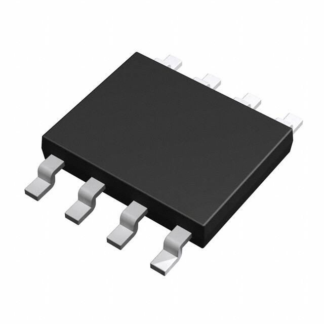
8-pin plastic SOP (P-SOP8-200-1.27-T2K)
• RoHS (Restriction of hazardous substances) compliant
1/16
�FEDR44V064B-02
MR44V064B
PIN CONFIGURATION
8-pin plastic SOP
1
A1
2
A2
3
VSS
4
MR44V064B
A0
8
VCC
7
WP
6
SCL
5
SDA
PIN DESCRIPTIONS
Pin Name
A0 – A2
Description
Address ( input )
Address pin indicates device address. When Address value is match the device address
code from SDA, the device will be selected. The address pins are pulled down internally.
Serial data input serial data output ( input / output )
SDA
SDA is a bi-directional line for I2C interface. The output driver is open-drain. A pull-up
resistor is required.
Serial Clock ( input )
SCL
Serial Clock is the clock input pin for setting for serial data timing. Inputs are latched on
the rising edge and outputs occur on the falling edge.
Write protect ( input )
WP
VCC, VSS
Write Protect pin controls write-operation to the memory. When WP is high, all address in
the memory will be protected. When WP is low, all address in the memory will be written.
WP pin is pulled down internally.
Power supply
Apply the specified voltage to VCC. Connect VSS to ground.
2/16
�FEDR44V064B-02
MR44V064B
I2C BUS
The MR44V064B employs a bi-directional two-wire I2C BUS interface, works as a slave device.
An example of I2C interface system with MR44V064B
Pull-up
resistor
SCL
SDA
SCL SDA
I2C BUS
master
SCL SDA
SCL SDA
MR44V064B
MR44V064B
(slave)
(slave)
A2 A1 A0
A2 A1 A0
000
001
I2C BUS COMUNICATION
I2C BUS data communication starts by start condition input, and ends by stop condition input. Data is always
8bit long, acknowledge is always required after each byte. I2C BUS carries out data transmission with plural
devices connected by 2 communication lines of serial data ( SDA ) and serial clock ( SCL ).
1-7
SCL
8
9
1-7
8
9
1-7
8
9
SDA
ADDRESS
START
condition
R/W
ACK
DATA
ACK
DATA
ACK
STOP
condition
START CONDITION
Before executing each command, start condition ( start bit ) where SDA goes from “HIGH” down to “LOW”
when SCL is “HIGH” is necessary. MR44V064B always detects whether SDA and SCL are in start condition
( start bit ) or not, therefore, unless this condition is satisfied, any command is executed.
STOP CONDITION
Each command can be ended by SDA rising from “LOW” to “HIGH” when stop condition ( stop bit ),
namely,SCL is “HIGH”.
3/16
�FEDR44V064B-02
MR44V064B
ACKNOWLEDGE ( ACK ) SIGNAL
This acknowledge ( ACK ) signal is a software rule to show whether data transfer has been made normally or not.
In master and slave, the device (μ-COM at slave address input of write command, read command, and this IC at
data output of read command) at the transmitter (sending) side releases the bus after output of 8bit data.
The device (this IC at slave address input of write command, read command, and μ-COM at data output of read
command) at the receiver (receiving) side sets SDA “LOW” during 9 clock cycles, and outputs acknowledge
signal ( ACK signal) showing that it has received the 8bit data.
This IC, after recognizing start condition and slave address (8bit), outputs acknowledge signal ( ACK signal)
“LOW”.
Each write action outputs acknowledge signal ( ACK signal ) “LOW”, at receiving 8bit data ( word address and
write data ).
Each read action outputs 8bit data ( read data ), and detects acknowledge signal ( ACK signal ) “LOW”.
When acknowledge signal ( ACK signal ) is detect, and stop condition is not sent from the master (μ-COM) side,
this IC continues data output. When acknowledge signal ( ACK signal ) is not detected, this IC stops data
transfer, and recognizes stop condition ( stop bit ), and ends read action. And this IC gets in status.
SLAVE ADDRESS
Output slave address after start condition from master.
The significant 4 bits of slave address are used for recognizing a device type. The device code of this IC is fixed
to “1010”.
Next slave addresses (A2 A1 A0 … device address) are for selecting devices, and plural ones can be used on a
same bus according to the number of device addresses.
The most insignificant bit (R/W…READ/WRITE) of slave address is used for designating write or read action,
and is as shown below.
Setting R/W to 0
Setting R/W to 1
SCL
SDA
START
condition
write (setting 0 to word address setting of random read)
read
1
2
3
4
5
1
0
1
0
A2
6
A1
7
A0
8
9
1
2
R/W
ACK
WRITE PROTECT
When WP terminal is set Vcc(H level), data rewrite of all addresses is prohibited. When it is set Vss(L level),
data rewrite of all address is enabled. Be sure to connect this terminal to Vcc or Vss, or control it to H level or L
level. Because this terminal is pulled down internally, in the case of Open the terminal will be recognized as L
level
During write cycle WP terminal must be always “L” level. WP terminal must be fixed from start condition to
stop condition.
4/16
�FEDR44V064B-02
MR44V064B
COMMAND
BYTE WRITE CYCLE
Arbitrary data is written to FeRAM. When to write only 1 byte, byte write is normally used.
start condition
slave address with LSB is 0 (write)
1st and 2nd word address
byte of write data.
stop condition
S
T
A
R
T
Slave address
W
R
I
T
E
st
1 WORD address
1 0 1 0 A2 A1 A0
0 0 0
W
A
12
2
W
A
8
A
C
K
nd
WORD address
W
A
7
S
T
O
P
Write data
W
A
0
A
C
K
D
7
D
0
A
C
K
A
C
K
PAGE WRITE CYCLE
When to write continuous data of 2 bytes or more, simultaneous write is possible by page write cycle. The
address reaches the final address, the address will be rolled over to the first address. By page write cycle, up to
8,192 bytes data can be written. When data above the maximum bytes are sent, data from the first byte will be
overwritten.
S
T
A
R
T
Slave address
W
R
I
T
E
st
1 WORD address
1 0 1 0 A2 A1 A0
0 0 0
W
A
12
2
W
A
8
A
C
K
nd
WORD address
W
A
7
Write data
W
A
0
A
C
K
D
7
S
T
O
P
Write data
D
0
A
C
K
D
7
D
0
A
C
K
A
C
K
BYTE WRITE CYCLE ( HS-MODE )
The MR44V064B support a maximum 3.4MHz high speed mode. When HS-mode operation is needed, the
HS-mode command is required before any command. After the HS-mode command is issued, MR44V064B will
be the HS-mode, until stop condition is issued.
S
T
A
R
T
S
T
A
R
T
HS-mode command
0 0 0 0 1 X X X
Slave address
W
R
I
T
E
st
1 WORD address
1 0 1 0 A2 A1 A0
N
A
C
K
0 0 0
A
C
K
W
A
12
2
W
A
8
W
A
7
A
C
K
nd
WORD address
S
T
O
P
Write data
W
A
0
D
7
A
C
K
D
0
A
C
K
5/16
�FEDR44V064B-02
MR44V064B
RANDOM READ CYCLE
Random read cycle is a command to read data by designating address.
start condition
slave address with LSB is 0 (write)
1st and 2nd word address
start condition
slave address with LSB is 1 (read)
read out byte of data.
ACK to “H”
stop condition
S
T
A
R
T
Slave address
W
R
I
T
E
st
1 WORD address
1 0 1 0 A2 A1 A0
0 0 0
W
A
12
2
W
A
8
A
C
K
nd
S
T
A
R
T
WORD address
W
A
7
W
A
0
A
C
K
Slave address
R
E
A
D
Read data
1 0 1 0 A2 A1 A0
D
7
A
C
K
S
T
O
P
D
0
A
C
K
N
A
C
K
SEQUENTIAL READ CYCLE
When ACK signal “L” after D0 is detected, and stop condition is not sent from master side, the next address data
can be read in succession. The address reaches the final address, the address will be rolled over to the first
address.
S
T
A
R
T
Slave address
W
R
I
T
E
st
1 WORD address
1 0 1 0 A2 A1 A0
0 0 0
W
A
12
2
W
A
8
A
C
K
nd
S
T
A
R
T
WORD address
W
A
7
W
A
0
A
C
K
Slave address
R
E
A
D
Read data
1 0 1 0 A2 A1 A0
D
7
D
0
A
C
K
A
C
K
S
T
O
P
A
C
K
D
0
N
D
A
C
7
K
CURRENT READ CYCLE
Current read cycle is a command to read data of internal address register without designating address. When the
last read or write address is (n)-th address just before current read cycle, the current read command outputs data
of (n+1)-th address. The previous read or write sequence should be complete up to stop condition.
Just after POWER ON, the internal address resister is unstable.
S
T
A
R
T
Slave address
R
E
A
D
S
T
O
P
Read data
1 0 1 0 A2 A1 A0
D7
D0
A
C
K
N
A
C
K
CURRENT ADDRESS READ CYCLE ( HS-MODE )
The MR44V064B support a maximum 3.4MHz high speed mode. When HS-mode operation is needed, the
HS-mode command is required before any command. After the HS-mode command is issued, MR44V064B will
be the HS-mode, until stop condition is issued.
S
T
A
R
T
S
T
A
R
T
HS-mode command
0 0 0 0 1 X X X
Slave address
R
E
A
D
Read data
1 0 1 0 A2 A1 A0
N
A
C
K
S
T
O
P
D7
A
C
K
D0
N
A
C
K
6/16
�FEDR44V064B-02
MR44V064B
ELECTRICAL CHARACTERISTICS
ABSOLUTE MAXIMUM RATINGS
The application of stress (voltage, current, or temperature) that exceeds the absolute maximum rating may
damage the device. Therefore, do not allow actual characteristics to exceed any one parameter ratings
PIN VOLTAGES
Parameter
Symbol
Rating
Min.
Max.
Unit
Pin Voltage (Input Signal)
VIN
–0.5
VCC + 0.5
V
Pin Voltage (Input/Output
Voltage)
VINQ, VOUTQ
–0.5
VCC + 0.5
V
VCC
–0.5
4.0
V
Power Supply Voltage
Note
TEMPERATURE RANGE
Parameter
Symbol
Rating
Min.
Max.
Unit
Storage Temperature
Tstg
–55
125
°C
Operating Temperature
Topr
–40
85
°C
Note
OTHERS
Parameter
Power Dissipation
Symbol
Rating
Note
PD
1,000mW
Ta=25°C
7/16
�FEDR44V064B-02
MR44V064B
RECOMMENDED OPERATING CONDITIONS
POWER SUPPLY VOLTAGE
Symbol
Min.
Typ.
Max.
Unit
Power Supply Voltage
VCC
1.8
3.3
3.6
V
Ground Voltage
VSS
0
0
0
V
Parameter
Note
DC INPUT VOLTAGE
Symbol
Min.
Max.
Unit
Input High Voltage
VIH
VCC x 0.7
VCC+0.3
V
Input Low Voltage
VIL
–0.3
VCC x 0.3
V
Parameter
Note
8/16
�FEDR44V064B-02
MR44V064B
DC CHARACTERISTICS
DC INPUT/OUTPUT CHARACTERISTICS
Symbol
Condition
Min.
Max.
Unit
VOL
IOL =3mA
―
0.4
V
Input Leakage Current
ILI
―
–10
10
µA
Output Leakage
Current
ILO
―
–10
10
µA
Parameter
Output Low Voltage
Note
POWER SUPPLY CURRENT
VCC=Max.to Min, Ta=Topr
Parameter
Symbol
Power Supply
Current
(Standby)
ICCS
Power Supply
Current
(Operating)
ICCA
Condition
SCL,SDA= VCC,
A2,A1,A0,WP= VCC or VSS
fSCL=3.4MHz
fSCL=1MHz
Max.
Unit
10
µA
1
300
mA
uA
Note
9/16
�FEDR44V064B-02
MR44V064B
AC CHARACTERISTICS
VCC=Max. to Min., Ta=Topr.
F/S-mode
Parameter
Symbol
F/S-mode
Plus
HS-mode
Min.
Max.
Min.
Max.
Min.
Max.
400
D.C.
1000
DC
3400
Unit
Clock frequency
fSCL
D.C.
Clock Low time
tLOW
1300
500
160
ns
Clock High time
tHIGH
600
300
60
ns
Output Data delay time
BUS release time before transfer start
tAA
900
450
130
Note
KHz
ns
tBUF
1300
500
300
ns
Start condition hold time
tHD:STA
600
250
160
ns
Start condition setup time
tSU:STA
600
250
160
ns
Input data hold time
tHD:DAT
0
0
0
ns
Input data setup time
tSU:DAT
100
100
10
ns
SDA, SCL rise time
tR
300
300
80
ns
1
SDA, SCL fall time
tF
300
100
80
ns
1
Stop condition setup time
tSU:STO
600
250
160
ns
Output data hold time
tDH
0
0
0
ns
Noise removal time (SDA, SCL)
tSP
50
50
5
ns
Note: 1. Not 100% tested
Equivalent AC Load Circuit
3.3V
1.1kΩ
Output
100pF
10/16
�FEDR44V064B-02
MR44V064B
TIMING
1/fSCL
tR
tF
SCL
VIL
tF
SDA
(input)
VIH
VIL
SDA
(input)
tSU:DAT
tSP
VIH VIH
VIH
VIL VIL
VIL
tLOW
tR
tSP
VIH
VIL
VIL
tHD:DAT
VIH
VIH
VIL
VIL
tBUF
SDA
(output)
SCL
tHIGH
VIH VIH
tAA
VIH
VIH
tSU:STA
tHD:STA
tDH
VIH
VIH
VIL
VIL
VIH
tSU:STO
VIH
VIL
START BIT
VIL
STOP BIT
11/16
�FEDR44V064B-02
MR44V064B
•POWER-ON AND POWER-OFF CHARACTERISTICS
Parameter
Power-On SCL,SDA High Hold Time
Power-Off SCL, SDA High Hold Time
Power-On Interval Time
VCC Power-On ramp rate
VCC Power-Off ramp rate
Symbol
tVHEL
tEHVL
tVLVH
tr
tf
(Under recommended operating conditions)
Min.
100
0
0
30
30
Max.
⎯
⎯
⎯
Unit
ns
ns
μs
μs/V
μs/V
Note
1, 2
1
2
Notes:
1. To prevent an erroneous operation, be sure to maintain SCL=SDA="H", and set the FeRAM in an inactive
state (standby mode) before and after power-on and power-off.
2. Powering on at the intermediate voltage level will cause an erroneous operation; thus, be sure to power up
from 0 V.
3. Enter all signals at the same time as power-on or enter all signals after power-on.
•Power-On and Power-Off Sequences
tEHVL
tVHEL
VCC
VCC
VCC Min.
VIH Min.
VCC Min.
tf
tr
VIH Min.
tVLVH
VIL Max.
SCL,SDA
0V
VIL Max.
SCL,SDA
0V
•After Power-Off, terminal state
When MR44V064B only goes power-off while the other IC’s on I2C bus are active, all the input pins including
I/O pin of MR44V064B must be GND level.
12/16
�FEDR44V064B-02
MR44V064B
READ/WRITE CYCLES AND DATA RETENTION
(Under recommended operating conditions)
Parameter
Min.
12
10
10
Read/Write Cycle
Data Retention
Max.
⎯
⎯
Unit
Cycle
Year
Note
CAPACITANCE
Vcc=3.3V, VIN = VOUT = GND, f = 1MHz, and Ta = 25°C
Signal
Input Capacitance
Input/Output Capacitance
Symbol
CIN
COUT
Min.
⎯
⎯
Max.
10
10
Unit
pF
pF
Note
1
1
Note:
1. Sampling value.
13/16
�FEDR44V064B-02
MR44V064B
PACKAGE DIMENSIONS
(Unit: mm)
Notes for Mounting the Surface Mount Type Package
The surface mount type packages are very susceptible to heat in reflow mounting and humidity absorbed in
storage. Therefore, before you perform reflow mounting, contact a ROHM sales office for the product name,
package name, pin number, package code and desired mounting conditions (reflow method, temperature and
times).
14/16
�FEDR44V064B-02
MR44V064B
REVISION HISTORY
Page
Document No.
FEDR44V064B-01
FEDR44V064B-02
Date
Previous
Edition
Current
Edition
Description
Jan. 08, 2016
–
–
Final edition 1
Sep. 07,2017
–
9
11
12
–
9
11
12
Corrected a vague description.
Corrected a condition of power supply current
Added VIH/VIL
Added “After Power-Off, terminal state”
15/16
�FEDR44V064B-02
MR44V064B
Notes
1) The information contained herein is subject to change without notice.
2) Although LAPIS Semiconductor is continuously working to improve product reliability and quality,
semiconductors can break down and malfunction due to various factors. Therefore, in order to prevent
personal injury or fire arising from failure, please take safety measures such as complying with the
derating characteristics, implementing redundant and fire prevention designs, and utilizing backups and
fail-safe procedures. LAPIS Semiconductor shall have no responsibility for any damages arising out of
the use of our Products beyond the rating specified by LAPIS Semiconductor.
3) Examples of application circuits, circuit constants and any other information contained herein are
provided only to illustrate the standard usage and operations of the Products. The peripheral conditions
must be taken into account when designing circuits for mass production.
4) The technical information specified herein is intended only to show the typical functions of the
Products and examples of application circuits for the Products. No license, expressly or implied, is
granted hereby under any intellectual property rights or other rights of LAPIS Semiconductor or any
third party with respect to the information contained in this document; therefore LAPIS Semiconductor
shall have no responsibility whatsoever for any dispute, concerning such rights owned by third parties,
arising out of the use of such technical information.
5) The Products are intended for use in general electronic equipment (i.e. AV/OA devices, communication,
consumer systems, gaming/entertainment sets) as well as the applications indicated in this document.
6) The Products specified in this document are not designed to be radiation tolerant.
7) For use of our Products in applications requiring a high degree of reliability (as exemplified below),
please contact and consult with a LAPIS Semiconductor representative: transportation equipment (i.e.
cars, ships, trains), primary communication equipment, traffic lights, fire/crime prevention, safety
equipment, medical systems, servers, solar cells, and power transmission systems.
8) Do not use our Products in applications requiring extremely high reliability, such as aerospace
equipment, nuclear power control systems, and submarine repeaters.
9) LAPIS Semiconductor shall have no responsibility for any damages or injury arising from
non-compliance with the recommended usage conditions and specifications contained herein.
10) LAPIS Semiconductor has used reasonable care to ensure the accuracy of the information contained in
this document. However, LAPIS Semiconductor does not warrant that such information is error-free
and LAPIS Semiconductor shall have no responsibility for any damages arising from any inaccuracy or
misprint of such information.
11) Please use the Products in accordance with any applicable environmental laws and regulations, such
as the RoHS Directive. For more details, including RoHS compatibility, please contact a ROHM sales
office. LAPIS Semiconductor shall have no responsibility for any damages or losses resulting
non-compliance with any applicable laws or regulations.
12) When providing our Products and technologies contained in this document to other countries, you
must abide by the procedures and provisions stipulated in all applicable export laws and regulations,
including without limitation the US Export Administration Regulations and the Foreign Exchange and
Foreign Trade Act.
13) This document, in part or in whole, may not be reprinted or reproduced without prior consent of LAPIS
Semiconductor.
Copyright 2017 LAPIS Semiconductor Co., Ltd.
2-4-8 Shinyokohama, Kouhoku-ku,
Yokohama 222-8575, Japan
http://www.lapis-semi.com/en/
16/16
�


 工商网监
湘ICP备2023018690号
工商网监
湘ICP备2023018690号
