Dear customer
LAPIS Semiconductor Co., Ltd. ("LAPIS Semiconductor"), on the 1st day of October,
2020, implemented the incorporation-type company split (shinsetsu-bunkatsu) in which
LAPIS established a new company, LAPIS Technology Co., Ltd. (“LAPIS
Technology”) and LAPIS Technology succeeded LAPIS Semiconductor’s LSI business.
Therefore, all references to "LAPIS Semiconductor Co., Ltd.", "LAPIS Semiconductor"
and/or "LAPIS" in this document shall be replaced with "LAPIS Technology Co., Ltd."
Furthermore, there are no changes to the documents relating to our products other than
the company name, the company trademark, logo, etc.
Thank you for your understanding.
LAPIS Technology Co., Ltd.
October 1, 2020
�FEDR45V
V100A-01
Isssue Date: Sep. 4, 2017
MR
R45V1100A
1M Bit((131,072-Worrd × 8-Bit) FeR
RAM (Ferroellectric Random
m Access Mem
mory)
SPI
GENER
RAL DESCR
RIPTION
The MR445V100A is a nonvolatile 128Kword
1
x 88-bit ferroelecctric random access
a
memorry (FeRAM) developed
in the feerroelectric prrocess and sillicon-gate CM
MOS technolo
ogy. The MR
R45V100A iss accessed using Serial
Peripheraal Interface. Unlike
U
SRAMss, this device, whose cells are
a nonvolatilee, eliminates bbattery backup
p required
to hold ddata. This devvice has no mechanisms
m
off erasing and programming
g memory cel
ells and block
ks, such as
those useed for variouss EEPROMs. Therefore, th e write cycle time can be equal to the rread cycle tim
me and the
power coonsumption duuring a write can
c be reducedd significantly
y.
The MR445V100A can be used in vaarious applicattions, becausee the device is guaranteed foor the write/reead
tolerance of 1012 cycles per bit and the
t rewrite couunt can be exttended significcantly.
FEATUR
RES
•
•
•
•
•
•
•
131,0722-word × 8-bitt configuration (Serial Perippheral Interface: SPI)
A single 1.8V to 3.6V
V (3.3V typ.)
) power suppply
READ cycle) / 40MHz(Exccept for READ
D)
Operatiing frequency:
34MHz(R
Read/w
write tolerance
1012 cyclees/bit
Data rettention
10 years
Guarantteed operatingg temperature range
5°C
−40 to 85
Low poower consumpption
Power supply currennt (@40MHz)
3.0mA(T
Typ.),
4.5mA(Max.)
Standbby mode supplly current
10μA(Ty
yp.),
50
0μA(Max.)
Sleep m
mode supply current
c
0.1μA(Ty
yp.),
2μ
μA(Max.)
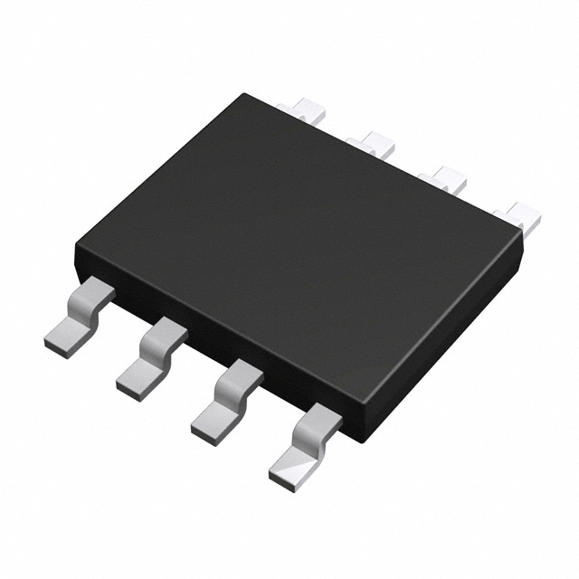
• Packagee options:
8-ppin plastic SO
OP (P-SOP8-200-1.27-T2K))
8-ppin plastic DIP
P (P-DIP8-300-2.54-T6)
• RoHS ((Restriction off hazardous su
ubstances) com
mpliant
1/21
�FEDR45V100A-01
MR45V100A
PIN CONFIGURATION (Top View)
8-pin plastic SOP / DIP
1
SO
2
WP#
3
VSS
4
MR45V100A
CS#
8
VCC
7
HOLD#
6
SCK
5
SI
Note:
Signal names that end with # indicate that the signals are negative-true logic.
PIN DESCRIPTIONS
Pin Name
Description
CS#
Chip Select (input, negative logic)
Latches an address by low input, activates the FeRAM, and enables read or write
operation. High input goes the device disable state.
WP#
Write Protect( input, negative logic )
Write Protect pin controls write-operation to the status-register(BP0,BP1). This pin should
be fixed low or high in write-operations.
HOLD#
HOLD( input, negative logic )
Hold pin is used when the serial-communication suspended without disable the chip
select. When HOLD# is low, the serial-output is in High-Z status and
serial-input/serial-clock are “Don’t Care”. CS# should be low in hold operation.
SCK
Serial Clock
Serial Clock is the clock input pin for setting for serial data timing. Inputs are latched on the
rising edge and outputs occur on the falling edge.
SI
Serial input
SI pins are serial input pins for Operation-code, addresses, and data-inputs.
SO
VCC, VSS
Serial output
SO pins are serial output pins.
Power supply
Apply the specified voltage to VCC. Connect VSS to ground.
2/21
�FEDR45V100A-01
MR45V100A
SPI MODE (Serial Peripheral Interface)
SPI mode0(CPOL=0, CPHA=0)
CS#
SCK
SI
MSB
LSB
SPI mode3(CPOL=1, CPHA=1)
CS#
SCK
SI
MSB
LSB
STATUS REGISTER
b7
b0
SRWD
0
0
0
BP1
BP0
WEL
WIP
Status Register Write Disable
Block Protect Bits
Write Enable Latch
Write In Progress (Always 0)
Name
Function
WIP
WEL
BP0,BP1
Fixed to 0.
Write Enable Latch. This indicates internal WEL condition.
Block Protect: These bits can change protected area.
This is the software protect.
SRWD
Status Register Write Disable(SRWD): SRWD controls the effect of the hardware
WP# pin. This device will be in hardware-protect by combination of SRWD and
WP#.
Fixed to 0.
0
3/21
�FEDR45V100A-01
MR45V100A
OPERATION-CODE
Operation codes are listed in the table below. If the device receives invalid operation code, the device will be
deselected.
Instruction
Description
Instruction format
WREN
Write Enable
0000 0110
WRDI
Write Disable
0000 0100
RDSR
Read Status Register
0000 0101
WRSR
Write Status Register
0000 0001
READ
Read from Memory Array
0000 0011
WRITE
Write to Memory Array
0000 0010
FSTRD
Fast Read from Memory Array
0000 1011
RDID
Read device ID
1001 1111
SLEEP
Enter Sleep Mode
1011 1001
4/21
�FEDR45V100A-01
MR45V100A
COMMANDS
WREN (Write Enable)
It is necessary to set Write Enable Latch(WEL)bit before write-operation (WRITE and WRSR).
WREN command sets WEL bit.
CS#
WP#
Fixed “H”
0
1
2
3
4
5
6
7
SCK
SI
SO
High-Z
WRDI (Write Disable)
WRDI command resets WEL bit.
CS#
WP#
Fixed “H”
0
1
2
3
4
5
6
7
SCK
SI
SO
High-Z
5/21
�FEDR45V100A-01
MR45V100A
RDSR (READ Status Register)
The RDSR command allows reading data of status register. The Status Register can be read anytime and any
number of times.
CS#
WP#
Fixed “H”
0
1
2
3
4
5
6
7
8
9
10
11
12
13
14
15
7
6
5
4
3
2
1
0
SRWD 0
0
0
SCK
SI
SO
High-Z
7
BP1 BP0 WEL WIP SRWD
WRSR (WRITE Status Register)
WRSR command allows to write data to status register(SRWD,BP0,BP1). It is necessary to set Write Enable
Latch(WEL)bit by WREN command before executing WRSR. WRSR command cannot write RFU(b6,b5,b4),
WEL(b1), WIP(b0) of Status Resistor..
CS#
0
1
2
3
4
5
6
7
8
9
10
11
12
13
14
15
7
6
5
4
3
2
1
0
SRWD X
X
X
X
X
SCK
SI
SO
BP1 BP0
High-Z
Note:
WP#=Fixed ”H”
6/21
�FEDR45V100A-01
MR45V100A
READ (Read from Memory Array)
READ command can be valid when CS# goes “L”, then the op-code and 24bit-addresses are inputted to serial
input ”SI”. The inputted addresses are loaded to internal register, then the data from corresponded address is
outputted at serial-output “SO”. If CS# will keep “L”, the internal address will be increased automatically after
8 clocks and will output the data from new-address. When it reaches the most significant address, the address
counter rolls over to starting address, and reading cycle can be continued infinitely. To finish read cycle, make
the CS# “H” during LSB output clock.
CS#
0
1
2
3
4
5
6
7
8
9
14
23
22
17
X
X
X
15
16
16
15
28
29
30
31
SCK
SI
A16 A15
3
2
1
0
A3
A2
A1
A0
m-2
m-1
24bit Address (An)
SO
High-Z
CS#
32
33
34
35
36
37
38
39
40
41
42
Q7
Q6
Q5
Q4
Q3
Q2
Q1
Q0
Q7
Q6
Q5
43
44
45
46
47
Q4
Q3
Q2
Q1
Q0
m
SCK
SI
SO
Q2
Q1
Q0
Data Out (An+1)
Data Out (An)
Note : WP# = fixed ”H”
FSTRD (Fast Read from Memory Array)
FSTRD command can be valid when CS# goes “L”, then the op-code and 24bit-addresses are inputted to serial
input ”SI”. After 8bits for dummy byte, the data from corresponded address is outputted at serial-output “SO”.
If CS# will keep “L”, the internal address will be increased automatically after 8 clocks and will output the data
from new-address. When it reaches the most significant address, the address counter rolls over to starting address,
and reading cycle can be continued infinitely. To finish read cycle, make the CS# “H” during LSB output
clock.
CS#
0
1
2
3
4
5
6
7
8
9
14
15
16
28
29
30
31
23
22
17
16
15
3
2
1
0
A3
A2
A1
A0
m-1
m
SCK
SI
X
X
A16 A15
X
24bit Address (An)
SO
High-Z
CS#
32
33
34
35
36
37
38
39
40
41
42
43
44
45
46
47
Q7
Q6
Q5
Q4
Q3
Q2
Q1
Q0
SCK
SI
SO
Dummy Byte
Note : WP# = fixed ”H”
Q1
Q0
Data Out (An)
7/21
�FEDR45V100A-01
MR45V100A
WRITE (Write to Memory Array)
Write command can be valid when CS# goes “L”, then the op-code and 24bit-addresses are inputted to serial
input ”SI”. Writing is terminated when CS# goes high after data-input. If CS# will keep “L”, the internal
address will be increased automatically. When it reaches the most significant address, the address counter rolls
over to starting address 0000h,and writing cycle(overwriting) can be continued infinitely. To finish write cycle,
make CS# “H” during LSB input clock.
WRITE (1Byte)
CS#
0
1
2
3
4
5
6
7
8
9
14
15
16
28
29
30
31
23
22
17
16
15
3
2
1
0
A3
A2
A1
A0
28
29
30
31
SCK
SI
X
X
A16 A15
X
24bit Address An
CS#
32
33
34
35
36
37
38
39
D7
D6
D5
D4
D3
D2
D1
D0
SCK
SI
Data In (An)
Note : WP# = Fixed ”H” , SO=High-Z
WRITE (Page)
CS#
0
1
2
3
4
5
6
7
8
9
14
23
22
17
X
X
X
15
16
16
15
SCK
SI
A16 A15
3
2
1
0
A3
A2
A1
A0
24bit Address An
CS#
32
33
34
35
36
37
38
39
40
41
42
43
44
45
46
47
D7
D6
D5
D4
D3
D2
D1
D0
D7
D6
D5
D4
D3
D2
D1
D0
D5
D4
D3
SCK
SI
Data In (An)
Data In (An+1)
CS#
48
49
50
51
52
53
54
55
D7
D6
D5
D4
D3
D2
D1
D0
SCK
SI
Data In (An+2)
D7
D6
D2
D1
D0
Data In (An+m)
Note : WP# = Fixed ”H” , SO=High-Z
8/21
�FEDR45V100A-01
MR45V100A
WRITE PROTECTION
Writing protection block is shown as follows: When Status Resister Write Disable(SRWD) bit is reset to “0”,
Status Resister number can be changed
Protect Block size
Block Protect BIT
BP1
BP0
0
0
1
1
0
1
0
1
Protected Block
None
Upper 1/4 block
Upper 1/2 block
All
Protected Address Area
None
18000h – 1FFFFh
10000h – 1FFFFh
00000h – 1FFFFh
Writing Protect
WP#
1
SRWD
mode
0
0
0
1
1
0
1
Writing protection status
in status register
Protection status in memory
Unprotected
Protected blocks
blocks
Software
protection
(SPM)
Status register is
unprotected when
WEL-bit is set by WREN
command. BP0 and BP1
are unprotected.
Protected
Unprotected
Hardware
protection
(HPM)
Status register is
protected. BP0 and BP1
are protected.
Protected
Unprotected
9/21
�FEDR45V100A-01
MR45V100A
HOLD
Hold status is used for suspending serial communication without disable the chip. SO becomes “High-Z” and SI
is “Don’t care” during the hold status. It is necessary to keep CS#=L in hold status.
Hold status
Hold status
SCK
HOLD#
RDID (Read device ID)
RDID command can be valid when CS# goes “L”, then the op-code are inputted to serial input ”SI”. Then
3bytes of device ID is output at serial-output “SO”.
Manufacture ID ( LAPIS )
Device type ( MR45V100A )
1st Byte
2nd Byte
3rd Byte
AEh
83h
09h
CS#
0
1
2
3
4
5
6
7
8
9
10
11
12
13
14
15
1
1
1
0
SCK
SI
1st Byte
SO
1
0
1
0
CS#
16
17
18
19
20
21
22
23
24
25
26
27
28
29
30
31
0
0
1
SCK
SI
2nd Byte
SO
1
0
0
0
rd
3 Byte
0
0
1
1
0
0
0
0
1
Note : WP# = Fixed ”H”
10/21
�FEDR45V100A-01
MR45V100A
SLEEP
SLEEP command transits MR45V100A to SLEEP Mode, and becomes low current consumption status.
Enter Sleep Mode
(1) Send SLEEP command “B9h”.
(2) MR45V100A starts transition to SLEEP mode after rising edge of CS#.
After the command is determined at 7th clock of SCK, SCK and SI input becomes “Don’t care” and
transit to SLEEP mode at the rising edge of CS#.
While CS# keeping “High” level, MR45V100A maintains SLEEP mode.
Exit Sleep Mode
(1) When CS# falling to Low level, MR45V100A start returning SLEEP Mode.
(2) When the time of tREC being after CS# falling, the return operation from SLEEP mode is finished and
command can be input.
And, before the time of tREC, the confirmation of returning is possible by doing dummy read.
tSHSL_SL
tREC
CS#
SCK
SI
SO
0
1
2
3
4
5
6
7
1 0
1
1
1
0 0
1
0
1
2
3
4
VALID
Hi
↑Enter SLEEP
Mode
↑Start of return ↑Exit SLEEP
from SLEEP Mode
11/21
�FEDR45V100A-01
MR45V100A
ELECTRICAL CHARACTERISTICS
ABSOLUTE MAXIMUM RATINGS
The application of stress (voltage, current, or temperature) that exceeds the absolute maximum rating may
damage the device. Therefore, do not allow actual characteristics to exceed any one parameter ratings
PIN VOLTAGES
Parameter
Pin Voltage (Input Signal)
Pin Voltage (Input/Output Voltage)
Power Supply Voltage
Rating
Symbol
Unit
Min.
Max.
VIN
–0.5
VCC + 0.5
V
VINQ, VOUTQ
–0.5
VCC + 0.5
V
VCC
–0.5
4.0
V
TEMPERATURE RANGE
Parameter
Symbol
Rating
Min.
Max.
Unit
Storage Temperature
Tstg
–55
125
°C
Operating Temperature
Topr
–40
85
°C
Note
OTHERS
Parameter
Power Dissipation
Symbol
Rating
Note
PD
1,000mW
Ta=25°C
12/21
�FEDR45V100A-01
MR45V100A
RECOMMENDED OPERATING CONDITIONS
POWER SUPPLY VOLTAGE
Symbol
Min.
Typ.
Max.
Unit
Power Supply Voltage
VCC
1.8
3.3
3.6
V
Ground Voltage
VSS
0
0
0
V
Parameter
DC INPUT VOLTAGE
Symbol
Min.
Max.
Unit
Input High Voltage
VIH
VCC x 0.7
VCC+0.3
V
Input Low Voltage
VIL
–0.3
VCC x 0.3
V
Parameter
OVERSHOOT/UNDERSHOOT TOLERANCE (Input signal)
Symbol
Pulse Width
Peak
“H” input
VIH OVERSHOOT
≤ 20ns
VCC+1.0V
“L” input
VIL UNDERSHOOT
≤ 20ns
– 1.0V
Parameter
13/21
�FEDR45V100A-01
MR45V100A
DC CHARACTERISTICS
DC INPUT/OUTPUT CHARACTERISTICS
Symbol
Condition
Min.
Max.
Unit
Output High Voltage
VOH
IOH =–2mA
VCC×0.85
―
V
Output Low Voltage
VOL
IOL =2mA
―
VCC×0.15
V
Input Leakage Current
ILI
―
–10
10
µA
Output Leakage
Current
ILO
―
–10
10
µA
Parameter
Note
POWER SUPPLY CURRENT
VCC=Max.to Min, Ta=Topr
Parameter
Symbol
Power Supply Current
(Standby)
ICCS
Power Supply Current
(Sleep)
IZZ
Power Supply Current
(Operating)
ICCA
Min.
Typ.
Max.
Unit
Note
CS#= VCC,
Other input terminals:
VIN=0V or VCC
―
10
50
µA
1
CS#=VCC,
Other input terminals :
VIN=0V or VCC
―
0.1
2
µA
1
SCK=40MHz,
IOUT=0mA
―
3
4.5
mA
1
Condition
Note: 1. Average electric current.
14/21
�FEDR45V100A-01
MR45V100A
AC CHARACTERISTICS
SPI mode AC characteristics
VCC=Max. to Min., Ta=Topr.
Parameter
Symbol
Read Cycle
Min.
Max.
Except for READ
Min.
Max.
Unit
Note
Clock frequency
fC
D.C.
34
D.C.
40
MHz
CS# setup time
tSLCH
10
―
10
―
ns
CS# De-select time
tSHSL
10
―
10
―
ns
tSHSL_SL
300
―
300
―
ns
tCHSH
10
―
10
―
ns
SCK High time
tCH
13
―
11
―
ns
1
SCK Low time
tCL
13
―
11
―
ns
1
Data Setup time
tDVCH
5
―
5
―
ns
Data Hold time
tCHDX
5
―
5
―
ns
SCK Low Hold time
after HOLD# inactive
SCK Low Hold time
after HOLD# active
SCK High Setup time
before HOLD# active
SCK High Setup time
before HOLD#
inactive
tHHCH
10
―
10
―
ns
tHLCH
10
―
10
―
ns
tCHHL
10
―
10
―
ns
tCHHH
10
―
10
―
ns
Output disable time
tSHQZ
―
12
―
12
ns
2
SCK Low to Output
Valid time
tCLQV
―
12
―
9
ns
VCC≧2.7V
―
13
―
10
ns
VCC


 工商网监
湘ICP备2023018690号
工商网监
湘ICP备2023018690号
