Rev.1.2_00
CMOS TEMPERATURE SENSOR IC
S-58LM20A Series
The S-58LM20A Series is a high-accuracy temperature sensor IC on a single chip, provides output voltage which is linear against the temperature change. Each chip consists of a temperature sensor, a constant current circuit, and an operational amplifier. This IC is able to be used under the wide temperature range of –55°C to 130°C. This IC has much better linearity than other conventional temperature sensors such as thermistor, it is possible to achieve the extensive application for temperature control.
Features
• Accuracy against temperature • Linear output voltage ±2.5°C (−55 to +130°C) −11.77 mV/°C Typ. Ta = −30°C: 2.205 V Typ. Ta = +30°C: 1.515 V Typ. Ta = +130°C: 0.303 V Typ. ±0.4% Typ. (−20 to +80°C) VDD = 2.4 to 5.5 V (−30 to +130°C) VDD = 2.7 to 5.5 V (−55 to +130°C) 4.5 µA Typ. (+25°C) 6.0 µA Max. (−55 to +130°C)
• Nonlinearity • Operation in wide range of power supply voltage • • • • • Low current consumption Built-in operational amplifier Output voltage referred to VSS Small package Lead-free product
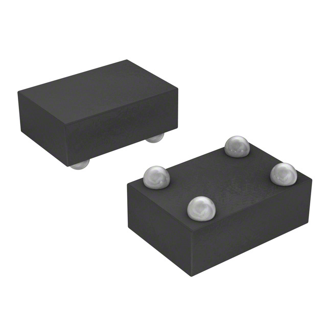
SNT-4A, SC-82AB, WLP-4B
Applications
• • • • • • • Compensation of high-frequency circuits such as cellular phones and radio equipment Compensation of oscillation frequency in crystal oscillator LCD contrast compensation Compensation of amplifier gain Compensation of auto focus circuits Temperature detection in battery management Overheating prevention for charged batteries or halogen lights
Package
Package Name SC-82AB SNT-4A WLP-4B Drawing Code Package NP004-A PF004-A HB004-B Tape NP004-A PF004-A HB004-B Reel NP004-A PF004-A HB004-B Land PF004-A
Seiko Instruments Inc.
1
�CMOS TEMPERATURE SENSOR IC S-58LM20A Series Block Diagram
Rev.1.2_00
VDD
VOUT
Temperature sensor VSS
Figure 1
2
Seiko Instruments Inc.
�Rev.1.2_00 Product Name Structure
CMOS TEMPERATURE SENSOR IC S-58LM20A Series
• Users can select the product type in the S-58LM20A Series. Regarding the contents of the product name, refer to “1. Product name” and regarding details, refer to“2. Product name list”.
1. Product name (1) SC-82AB, SNT-4A package
S-58LM20A xxxx G Package name (abbreviation) and packing specifications N4T1 : SC-82AB, Tape I4T1 : SNT-4A, Tape Product name *1. Refer to the taping specifications.
*1
(2) WLP-4B package
S-58LM20A xxxx S Package name (abbreviation) and packing specifications*1 H4T1 : WLP-4B, Tape Product name *1. Refer to the taping specifications.
2. Product name list
Table 1 Product Name S-58LM20A-N4T1G S-58LM20A-I4T1G S-58LM20A-H4T1S Temperature Accuracy ±2.5°C ±2.5°C ±2.5°C Package SC-82AB SNT-4A WLP-4B
Seiko Instruments Inc.
3
�CMOS TEMPERATURE SENSOR IC S-58LM20A Series Pin Configuration
SC-82AB Top view 4 3
Rev.1.2_00
Table 2 Pin No. 1 2 3 4 Pin Name VDD VSS NC*1 VOUT Description Power supply pin GND pin No connection Output voltage pin
*1. The NC pin is electrically open. The NC pin can be connected to VDD and VSS.
1 2
Figure 2
SNT-4A Top view 1 2 4 3
Table 3 Pin No. 1 2 3 4 Pin Name VSS VDD VOUT NC*1 Description GND pin Power supply pin Output voltage pin No connection
*1. The NC pin is electrically open. The NC pin can be connected to VDD and VSS. Figure 3
W LP-4B Top view
Pin No. 1 2 3 4
Table 4 Pin Name VDD VSS*1 VSS*1 VOUT Description Power supply pin GND pin GND pin Output voltage pin
4 1
3 2
*1. Connect both VSS pins to GND.
Figure 4
W LP-4B Bottom view
1 4
2 3
Figure 5
4
Seiko Instruments Inc.
�Rev.1.2_00 Absolute Maximum Ratings
Table 5
CMOS TEMPERATURE SENSOR IC S-58LM20A Series
Item Power supply pin voltage Output voltage SC-82AB Power dissipation SNT-4A WLP-4B Operating ambient temperature Storage temperature Topr Tstg PD VDD
Symbol VOUT
(Ta = 25°C unless otherwise specified) Absolute Maximum Rating Unit VSS – 0.3 to VSS + 6.5 VSS – 0.3 to VDD + 0.3 350*1 300*1 290
*1
V V mW mW mW
°C °C
–55 to +130 –65 to +150
*1. When mounted on board [Mounted board] (1) Board size: 114.3 mm × 76.2 mm × t1.6 mm (2) Board name: JEDEC STANDARD51-7 Caution The absolute maximum ratings are rated values exceeding which the product could suffer physical damage. These values must therefore not be exceeded under any conditions.
Seiko Instruments Inc.
5
�CMOS TEMPERATURE SENSOR IC S-58LM20A Series Electrical Characteristics
Rev.1.2_00
Item Range of power supply voltage Output voltage VOUT = (−3.88 × 10⁻⁶ × T2) +(−1.15 × 10⁻² × T) +1.8639 V
Symbol VDD VOUT
Table 6 (Ta = 25°C, VDD = 2.7 V, IOUT = 0 A unless otherwise specified) Test Conditions Min. Typ. Max. Unit Circuit −30°C ≤ Ta ≤ +130°C −55°C ≤ Ta ≤ +130°C Ta = −30°C Ta = +30°C Ta = +130°C −30°C ≤ Ta ≤ +130°C −20°C ≤ Ta ≤ +80°C −55°C ≤ Ta ≤ +130°C
Temperature sensitivity VSE Nonlinearity ∆NL Operating temperature range Topr Current consumption IDD Current consumption − ∆IDD1 VDD = 2.4 V to 5.5 V Power supply voltage Current consumption − ∆IDD2 Temperature Line regulation ∆VOUT1 VDD = 2.4 V to 5.5 V Load regulation*1 ∆VOUT2 IOUT = 0 to 16 µA *1. Do not flow current into the output voltage pin.
2.4 2.7 2.177 1.486 0.272 −12.20 −55
2.205 1.515 0.303 −11.77 ±0.4 4.5
5.5 5.5 2.234 1.545 0.335 −11.40 130 6.0
V V V V V mV/°C % °C µA
µA
1 1 1 1 1 1 1 1 2 2
0.1
-11
nA/°C mV/V mV/µA
3.3 0.156
6
Seiko Instruments Inc.
�Rev.1.2_00 Test Circuit
1.
A VDD S-58LM20A Series VSS V
CMOS TEMPERATURE SENSOR IC S-58LM20A Series
VOUT
V
Figure 6 2.
VDD S-58LM20A Series VSS V V VOUT A
IOUT
Figure 7
Seiko Instruments Inc.
7
�CMOS TEMPERATURE SENSOR IC S-58LM20A Series Explanation of Terms
1. Output voltage (VOUT)
VOUT indicates the output voltage at Ta = −30°C, Ta = +30°C, and Ta = +130°C.
Rev.1.2_00
O utput voltage
Max.
Min.
−30°C
0 °C
+30°C Temperature [Ta]
+130°C
Figure 8
8
Seiko Instruments Inc.
�Rev.1.2_00
2. Temperature Sensitivity (VSE)
CMOS TEMPERATURE SENSOR IC S-58LM20A Series
VSE is the temperature coefficient of output voltage which is calculated from an output voltage when Ta = −30°C and Ta = +130°C. VSE is calculated from the following formula. VSE =
[V
OUT
− VOUT *2 160 *3
*1
]
Output voltage VOUT (when Ta = −30°C)
VSE
VOUT (when Ta = +130°C)
−30°C
0 °C
+30°C Temperature [Ta]
+130°C
Figure 9 *1. VOUT value at Ta = +130°C [V] *2. VOUT value at Ta = −30°C [V] *3. The difference of the temperature between Ta = +130°C and Ta = −30°C [°C]
Seiko Instruments Inc.
9
�CMOS TEMPERATURE SENSOR IC S-58LM20A Series
3. Nonlinearity (∆NL)
∆NL is the nonlinearity of output voltage. Its deviation with the approximation line is shown below. ∆NL is calculated from the following formula.
Rev.1.2_00
∆NL =
a*1 × 100 b*2
Output voltage a VOUT ( when −20°C) (B) Actual measured value b a a VOUT ( when +80°C) (A) Approximation line
−20°C
0°C Temperature [Ta]
+80°C
*1. The maximum deviation of the actual measurement of output voltage (B) and an approximation line (A) in temperature −20°C to +80°C. The approximation line is the one to be drawn so that “a” should be the minimum value. *2. The difference of the actual measured value of output voltage when −20°C and +80°C. Figure 10
4. Line regulation (∆VOUT1)
∆VOUT1 indicates the dependency of output voltage against input voltage. This indicates how much the output voltage varies when changing the input voltage after fixing the output current constant.
5. Load regulation (∆VOUT2)
∆VOUT2 indicates the dependency of output voltage against output current. This indicates how much the output voltage varies when changing output current after fixing the input voltage constant.
6. Current consumption – Power supply voltage (∆IDD1)
∆IDD1 indicates the dependency of current consumption against power supply voltage. This indicates how much current consumption varies when changing the temperature after fixing an output current constant.
7. Current consumption - Temperature (∆IDD2)
∆IDD2 indicates the dependency of current consumption against temperature. This indicates how much current consumption varies when changing the temperature after fixing an output current constant.
10
Seiko Instruments Inc.
�Rev.1.2_00 Precautions
CMOS TEMPERATURE SENSOR IC S-58LM20A Series
• Wire each pin of VDD, VSS and VOUT carefully in order to set them in low impedance when wiring an IC on a patterned board. • In this IC, if load capacitance of the VOUT pin is large, VOUT pin voltage may oscillate. It is recommended not to use an external capacitor between the VOUT and VSS pin. When using an external capacitor, set near the VOUT pin. When connecting an A/D converter etc. to the VOUT pin, the input pin capacitance of the A/D converter and the parasitic capacitance component between wires are included as load capacitance. To prevent oscillation, it is recommended to use the following output load condition.
Load capacitance of VOUT pin (CL1) : 300 pF or less
VDD
S-58LM20A Series VSS
VOUT
CIN
CL1
VOUT
Figure 11 Caution The above connection diagram and constant will not guarantee successful operation. Perform through evaluation using the actual application to set the constant.
Seiko Instruments Inc.
11
�CMOS TEMPERATURE SENSOR IC S-58LM20A Series
Rev.1.2_00
In this IC, it is necessary to add a capacitor from an output pin to GND with a series resistor in the ambience having excessive noise, as seen in Figure 12 and Figure 13. In the combination shown in Table 7, a time constant against heat of this IC is much later than the time constant composed of RC, therefore it does not affect on the response time of this IC. Table 7 RL2 (Ω) 200 470 680 1k CL2 (µF) 1 0.1 0.01 0.001
VDD
S-58LM20A Series VSS
VOUT
RL2 VOUT
CIN
CL2
Figure 12
VDD
S-58LM20A Series VSS
VOUT RL2 CL2
VOUT
CIN
Figure 13 Caution The above connection diagram and constant will not guarantee successful operation. Perform through evaluation using the actual application to set the constant.
12
Seiko Instruments Inc.
�Rev.1.2_00
CMOS TEMPERATURE SENSOR IC S-58LM20A Series
• For stabilization, set a capacitor (CIN) of approx. 0.1 µF between VDD and VSS pin. • Do not connect a pull-up resistor to the output pin. • The application condition for input voltage, output voltage and load voltage must not exceed the package power dissipation. • Do not apply an electrostatic discharge to this IC that exceeds the performance ratings of the built-in electrostatic protection circuit. • Regarding the current at the output pin, refer to load regulation and footnote *1 in Table 6 “ Electrical Characteristics”. • SII claims no responsibility for any disputes arising out of or in connection with any infringement by products including this IC of patents owned by a third party.
Seiko Instruments Inc.
13
�CMOS TEMPERATURE SENSOR IC S-58LM20A Series Characteristics (Typical Data)
1. Output voltage (VOUT) vs. Temperature (Ta)
3.0 2.5 2.0 1.5 1.0 0.5 0 −55 −40 −20 0 20 40 60 Ta [°C] 80 100 120 130
Rev.1.2_00
2. Current consumption (IDD) vs. Temperature (Ta)
5.0 4.8 4.6 4.4 4.2 4.0 3.8 3.6 3.4 3.2 3.0 VDD = 5.5 V
IDD [µA]
VOUT [V]
VDD = 2.7 V VDD = 2.4 V
−55 −40
−20
0
20
40 60 Ta [°C]
80
100
120 130
3. Error range of each temperature Difference between the temperature converted into approximation line and actual temperature [°C]
6 4 2 0 −2 −4 −6 −55 −40 −20 0 20 40 60 Ta [°C] 80 100 120 130
4. Current consumption (IDD) vs. Power supply voltage (VDD)
6 5 4 3 2 1 0 2.4 Ta = −30°C Ta = −55°C Ta = 30°C Ta = 130°C 3.0 3.5 4.0 4.5 VDD [V] 5.0 5.5
5. Output voltage (VOUT) vs. Power supply voltage (VDD)
2.210 2.209 2.208 2.207 2.206 2.205 2.204 2.203 2.202 2.201 2.200 2.4 3.0 3.5 Ta = −30°C
IDD [µA]
4.0 4.5 VDD [V]
5.0
5.5
1.520 1.519 1.518 1.517 1.516 1.515 1.514 1.513 1.512 1.511 1.510 2.4 3.0 3.5 4.0 4.5 VDD [V]
Ta = 30°C
VOUT [V]
VOUT [V]
5.0
5.5
0.310 0.309 0.308 0.307 0.306 0.305 0.304 0.303 0.302 0.301 0.300 2.4 3.0 3.5 4.0 4.5 VDD [V]
Ta = 130°C
VOUT [V]
5.0
5.5
14
Seiko Instruments Inc.
�Rev.1.2_00
CMOS TEMPERATURE SENSOR IC S-58LM20A Series
6. Output voltage (VOUT) vs. Load current (IOUT)
3.0 2.5 2.0 1.5 1.0 0.5 0 0 0.5 1.0 IOUT [mA] 1.5 2.0 VDD = 2.4 V Ta = −30°C Ta = 30°C Ta = 130°C 3.0 2.5 2.0 1.5 1.0 0.5 0 0 0.5 1.0 1.5 2.0 IOUT [mA] 2.5 3.0 VDD = 2.7 V Ta = −55°C Ta = 30°C Ta = 130°C
VOUT [V]
3.0 2.5 2.0 1.5 1.0 0.5 0 0 2.0 4.0 6.0 IOUT [mA]
VDD = 5.5 V Ta = −55°C Ta = 30°C Ta = 130°C
VOUT [V]
8.0
10.0
7. Heat response Output voltage (VOUT) vs. Time (t)
When packages are put into the air of 130°C from the air of 25°C 1.8 1.6 1.4 1.2 SC-82AB 1.0 SNT-4A 0.8 WLP-4B 0.6 0.4 0.2 0 0 20 40 60 80 100 120 140 160 160 200 220 240 t [s] When packages are put into the liquid of 130°C from the air of 25°C 1.8 1.6 1.4 WLP-4B 1.2 1.0 SC-82AB 0.8 SNT-4A 0.6 0.4 0.2 0 0 5 10 15 20 25 30 35 40 45 t [s]
VOUT [V]
8. Start up response
Ta = 25°C, CL = 100pF, RL = 10 MΩ Ta = 25°C, CL = 100pF, RL = 10 MΩ
VDD (= 5.5 V)
1 V / div. GND
VOUT [V]
VOUT [V]
VDD (= 2.4 V) VOUT t (50 µs / div.)
1 V / div. GND 1 V / div. GND
VOUT t (50 µs / div.)
1 V / div. GND
Seiko Instruments Inc.
15
�CMOS TEMPERATURE SENSOR IC S-58LM20A Series
Rev.1.2_00
Marking Specifications
1. SC-82AB
SC-82AB Top view 4 3
(1) to (3)
: Product code (refer to Product name vs. Product code)
(1)
(2)
(3)
1
2
Product name vs. Product code
Product name S-58LM20A-N4T1G
(1) D
Product code (2) (3) R E
2. SNT-4A
SNT-4A Top view 1 (1) (2) (3) 2 3 4
(1) to (3)
: Product code (refer to Product name vs. Product code)
Product name vs. Product code
Product name S-58LM20A-I4T1G
(1) D
Product code (2) (3) R E
16
Seiko Instruments Inc.
�2.0±0.2
4
1.3±0.2
3
0.05
1 2
0.16 -0.06
+0.1
0.3 -0.05
+0.1
0.4 -0.05
+0.1
No. NP004-A-P-SD-1.1
TITLE No. SCALE UNIT
SC82AB-A-PKG Dimensions NP004-A-P-SD-1.1
mm
Seiko Instruments Inc.
�ø1.5 -0
+0.1
4.0±0.1
2.0±0.05
4.0±0.1
1.1±0.1 0.2±0.05
ø1.05±0.1 (0.7)
2.2±0.2
2
1
3
4
Feed direction
No. NP004-A-C-SD-3.0
TITLE No. SCALE UNIT
SC82AB-A-Carrier Tape NP004-A-C-SD-3.0
mm
Seiko Instruments Inc.
�12.5max.
Enlarged drawing in the central part ø13±0.2
9.0±0.3
(60°)
(60°)
No. NP004-A-R-SD-1.1
TITLE No. SCALE UNIT mm
SC82AB-A-Reel NP004-A-R-SD-1.1
QTY. 3,000
Seiko Instruments Inc.
�1.2±0.04
4 3
1
2
+0.05 0.08 -0.02
0.65 0.48±0.02
0.2±0.05
No. PF004-A-P-SD-4.0
TITLE No. SCALE UNIT
SNT-4A-A-PKG Dimensions PF004-A-P-SD-4.0
mm
Seiko Instruments Inc.
�ø1.5 -0
+0.1
2.0±0.05
4.0±0.1
0.25±0.05
5°
1.45±0.1
ø0.5 -0
+0.1
4.0±0.1
0.65±0.05
2
1
3
4
Feed direction
No. PF004-A-C-SD-1.0
TITLE No. SCALE UNIT
SNT-4A-A-Carrier Tape PF004-A-C-SD-1.0
mm
Seiko Instruments Inc.
�12.5max.
Enlarged drawing in the central part ø13±0.2
9.0±0.3
(60°)
(60°)
No. PF004-A-R-SD-1.0
TITLE No. SCALE UNIT mm
SNT-4A-A-Reel PF004-A-R-SD-1.0
QTY. 5,000
Seiko Instruments Inc.
�0.52
1.16
0.52
0.3
0.35
0.3
Caution Making the wire pattern under the package is possible. However, note that the package may be upraised due to the thickness made by the silk screen printing and of a solder resist on the pattern because this package does not have the standoff.
No. PF004-A-L-SD-3.0
TITLE No. SCALE UNIT
SNT-4A-A-Land Recommendation
PF004-A-L-SD-3.0
mm
Seiko Instruments Inc.
�0.84±0.02
4
3
0.84±0.02
1
2
0.58max. 0.40±0.02
S 0.06 S ø0.20±0.02
0.58max.
0.13±0.03
(0.5) 4-(ø0.20) ø0.05 M S AB A 0.5
1
B
2
4
3
No. HB004-B-P-SD-1.0
TITLE No. SCALE UNIT
WLP-4B-B-PKG Dimensions HB004-B-P-SD-1.0
Seiko Instruments Inc.
�ø1.5 -0
+0.1
2.0±0.05
4.0±0.1
0.18±0.05
ø0.35±0.05
4.0±0.1
0.73±0.05
Count mark(R0.3,Depth 0.2) (Every 10 pockets) 1.16 1.1 0.7 0.93±0.05 0.95
2 3
1 4
Feed direction
No. HB004-B-C-SD-1.0
TITLE No. SCALE UNIT
WLP-4B-B-Carrier Tape HB004-B-C-SD-1.0
mm
Seiko Instruments Inc.
�12.5max.
9.0±0.3 Enlarged drawing in the central part ø13±0.2
No. HB004-B-R-SD-1.0
TITLE No. SCALE UNIT
WLP-4B-B-Reel HB004-B-R-SD-1.0
QTY. mm 3,000
Seiko Instruments Inc.
�• • • • • •
The information described herein is subject to change without notice. Seiko Instruments Inc. is not responsible for any problems caused by circuits or diagrams described herein whose related industrial properties, patents, or other rights belong to third parties. The application circuit examples explain typical applications of the products, and do not guarantee the success of any specific mass-production design. When the products described herein are regulated products subject to the Wassenaar Arrangement or other agreements, they may not be exported without authorization from the appropriate governmental authority. Use of the information described herein for other purposes and/or reproduction or copying without the express permission of Seiko Instruments Inc. is strictly prohibited. The products described herein cannot be used as part of any device or equipment affecting the human body, such as exercise equipment, medical equipment, security systems, gas equipment, or any apparatus installed in airplanes and other vehicles, without prior written permission of Seiko Instruments Inc. Although Seiko Instruments Inc. exerts the greatest possible effort to ensure high quality and reliability, the failure or malfunction of semiconductor products may occur. The user of these products should therefore give thorough consideration to safety design, including redundancy, fire-prevention measures, and malfunction prevention, to prevent any accidents, fires, or community damage that may ensue.
�


 工商网监
湘ICP备2023018690号
工商网监
湘ICP备2023018690号
