Si51211 Data Sheet
Three Output Factory Programmable Clock Generator
KEY FEATURES
The factory programmable Si51211 is a low power, small footprint and frequency flexible
programmable clock generator targeting low power, low cost and high volume consumer
and embedded applications. The device operates from a single crystal or an external
clock source and generates 1 to 3 outputs up to 170 MHz. The device is factory programmed to provide customized output frequencies and control input such as frequency
select, spread spectrum on, power down and output enable. Center spread spectrum
can also be programmed to reduce EMI to meet board level system requirements.
Applications
• 8 to 48 MHz crystal input
• Programmable FSEL, SSONb, PD, and OE
input functions
4
PLL with
Modulation
Control
XIN/
3
CLKIN
XOUT 2
VDD 1
• Accepts crystal or reference clock input
• 3 to 165 MHz reference clock input
• Digital still camera
• IP phone
• Smart meter
• Crystal/XO replacement
• EMI reduction
• Portable devices
VDDO 8
• Generates up to 3 CMOS clock outputs
from 3 to 170 MHz
To Pin 7
V-REG
To Core
Programmable
Configuration
Register
To Pin 4 and Pin 6
VSS 5
silabs.com | Smart. Connected. Energy-friendly.
Buffers,
Dividers,
and
Switch
Matrix
SSCLK1/
REFCLK/
OE/FSEL/
SSONb
SSCLK2/
6 OE/SSONb/PD
7
SSCLK3
(VDDO)
Rev. 1.0
�Si51211 Data Sheet
Feature List
1. Feature List
The Si51211 highlighted features are listed below.
• Generates up to 3 CMOS clock outputs from 3 to 170 MHz
• Accepts crystal or reference clock input
• 3 to 165 MHz reference clock input
• 8 to 48 MHz crystal input
• Programmable FSEL, SSONb, PD, and OE input functions
• Low power dissipation
silabs.com | Smart. Connected. Energy-friendly.
• Separate voltage supply pins
• VDD = 2.5 to 3.3 V
• VDDO = 1.8 to 3.3 V (VDDO < VDD)
• ±0.25%, ±0.5% or ±1% spread spectrum (center spread)
• Low cycle-cycle jitter
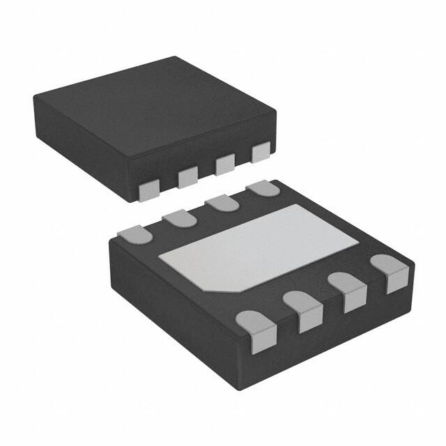
• Ultra small 8-pin TDFN package (1.4 mm x 1.6 mm)
Rev. 1.0 | 1
�Si51211 Data Sheet
Design Considerations
2. Design Considerations
2.1 Typical Application Schematic
2.2 Comments and Recommendations
Decoupling Capacitor: A decoupling capacitor of 0.1 μF must be used between VDD and VSS on pins 1 and 8. Place the capacitor on
the component side of the PCB as close to the VDD pin as possible. The PCB trace to the VDD pin and to the GND via should be kept
as short as possible. Do not use vias between the decoupling capacitor and the VDD pin. In addition, a 10 µF capacitor should be
placed between VDD and VSS.
Series Termination Resistor: A series termination resistor is recommended if the distance between the outputs (SSCLK or REFCLK
pins) and the load is over 1 ½ inches. The nominal impedance of the SSCLK output is about 30 Ω. Use a 20 Ω resistor in series with the
output to terminate a 50 Ω trace impedance and place a 20 Ω resistor as close to the SSCLK output as possible.
Crystal and Crystal Load: Only use a parallel resonant fundamental AT cut crystal. Do not use higher overtone crystals. To meet the
crystal initial accuracy specification (in ppm) make sure that the external crystal load capacitor is matched to the crystal load specification. To determine the value of CL1 and CL2, use the following formula:
CL1 = CL2 = 2CL − (Cpin + Cp);
where CL is the load capacitance stated by the crystal manufacturer,
Cpin is the Si51211 pin capacitance (3 pF), and
Cp is the parasitic capacitance of the PCB traces.
Example: If a crystal with CL = 12 pF specification is used and Cp = 1 pF (parasitic PCB capacitance on PCB), 19 or 20 pF external
capacitors from pins XIN (pin 2) and XOUT (Pin 3) to VSS are required. Users must verify Cp value.
Table 2.1. Crystal Specifications
Equivalent Series Resistance (ESR)
Crystal Output Capacitance (CO)
Load Capacitance (CL)
< 50 Ω
< 3 pF
< 13 pF
silabs.com | Smart. Connected. Energy-friendly.
Rev. 1.0 | 2
�Si51211 Data Sheet
Electrical Specifications
3. Electrical Specifications
Table 3.1. DC Electrical Specifications
(VDD = 2.5 V ±10%, or VDD = 3.3V ±-10%, VDDO = VDD, CL = 10 pF, TA = –40 to 85 °C)
Parameter
Symbol
Operating Voltage
VDD
Output High Voltage
Test Condition
Min
Typ
Max
Unit
VDD = 3.3 V ± 10%
2.97
3.3
3.63
V
VDD = 2.5 V ± 10%
2.25
2.5
2.75
V
VDDO
VDDO < VDD
1.71
—
3.6
V
VOH
IOH = –4 mA,
VDDX –
0.5
—
—
V
VDDX = VDD or VDDO
Output Low Voltage
VOL
IOL = 4 mA
—
—
0.3
V
Input High Voltage
VIH
CMOS Level
0.7 VDD
—
—
V
Input Low Voltage
VIL
CMOS Level
0
—
0.3 VDD
V
Operating Supply Current1
IDD
FIN = 12 MHz, SSCLK1 = 12 MHz,
SSCLK2 = 24 MHz, CL= 5 pF, VDD
= VDDO = 3.3 V
—
6.3
10
mA
IDDPD
—
0.5
0.65
mA
—
30
—
Ω
Pin 6
—
150k
—
Ω
Input pin capacitance
—
3
5
pF
—
—
10
pF
Power Down Current
Nominal Output Impedance
ZO
Internal Pull-up/Pull-down Resistor
RPUP/RPD
Input Pin Capacitance
CIN
Load Capacitance
CL
Note:
1. IDD depends on input and output frequency configurations.
Table 3.2. AC Electrical Specifications
(VDD = 2.5 V ±10%, or VDD = 3.3 V ±10%, VDDO = VDD, CL = 10 pF, TA = –40 to 85 °C)
Parameter
Symbol
Condition
Min
Typ
Max
Unit
Input Frequency Range
FIN1
Crystal input
8
—
48
MHz
Input Frequency Range
FIN2
Reference clock Input
3
—
165
MHz
Output Frequency Range
FOUT
SSCLK1/2/3
3
—
170
MHz
Frequency Accuracy
FACC
Configuration dependent
—
0
—
ppm
DCOUT
Measured at VDDO/2
45
50
55
%
40
50
60
%
30
50
70
%
Output Duty Cycle
FOUT < 75 MHz
Measured at VDDO/2
FOUT > 75 MHz
Input Duty Cycle
DCIN
silabs.com | Smart. Connected. Energy-friendly.
CLKIN, CLKOUT through PLL
Rev. 1.0 | 3
�Si51211 Data Sheet
Electrical Specifications
Parameter
Symbol
Condition
Min
Typ
Max
Unit
Output Rise/Fall Time
tr/tf
CL= 10 pF, 20 to 80%
—
1
2
ns
Period Jitter
PJ1
SSCLK1/2/3, at the same frequency
—
12
20
ps rms
PJ2
SSCLK1/2/3, at different output frequencies1
—
30
952
ps rms
CCJ1
SSCLK1/2/3, at the same frequency
—
85
150
ps
CCJ2
SSCLK1/2/3, at different output frequencies1
—
145
2902
ps
Power-up Time
tPU
Time from 0.9 VDD to valid
frequencies at all clock outputs
—
1.2
5
ms
Output Enable Time
tOE
Time from OE rising edge to active
at outputs SSCLK1/2 (asynchronous), FOUT = 133 MHz
—
15
—
ns
Output Disable Time
tOD
Time from OE falling edge to active
at outputs SSCLK1/2 (asynchronous), FOUT = 133 MHz
—
15
—
ns
—
37
—
kHz
Cycle-to-Cycle Jitter
Spread Spectrum Modulation Rate3
SSDEV
Note:
1. Example frequency configurations:
• 8 MHz, 100 MHz, 75 MHz
• 48 MHz, 100 MHz, 66 2/3 MHz
• 96 MHz, 133 1/3 MHz, 133 1/3 MHz
2. Jitter performance depends on configuration and programming parameters.
3. The SS modulation rate is a fixed ratio of the reference frequency with values in the range of 30 kHz to 50 kHz based on the
frequency plan.
Table 3.3. Absolute Maximum Conditions
Parameter
Symbol
Condition
Min
Typ
Max
Unit
–0.5
—
4.2
V
Main Supply Voltage
VDD
Input Voltage
VIN
Relative to VSS
–0.5
—
VDD+0.5
V
Temperature, Storage
TS
Non-functional
–65
—
150
°C
Temperature, Operating Ambient
TA
Functional, I-Grade
–40
—
85
°C
ESD Protection (Human Body Model)
ESDHBM
JEDEC (JESD 22-A114)
–4000
—
4000
V
ESD Protection (Charge Device
Model)
ESDCDM
JEDEC (JESD 22-C101)
–1500
—
1500
V
ESD Protection (Machine Model)
ESDMM
JEDEC (JESD 22-A115)
–200
—
200
V
Note:
1. While using multiple power supplies, the Voltage on any input or I/O pin cannot exceed the power pin during power-up. Power
supply sequencing is not required.
silabs.com | Smart. Connected. Energy-friendly.
Rev. 1.0 | 4
�Si51211 Data Sheet
Functional Description
4. Functional Description
4.1 Input Frequency Range
The input frequency range is from 8.0 to 48.0 MHz for crystals and ceramic resonators. If an external clock is used, the input frequency
range is from 3.0 to 165.0 MHz.
4.2 Output Frequency Range and Outputs
Up to three outputs can be programmed as SSCLK or REFCLK. SSCLK output can be synthesized to any value from 3 to 170 MHz with
spread based on valid input frequency. The spread at the SSCLK pins can be enabled or disabled by the SSONb input control pin. If
SSONb is used, when this pin is pulled high (VDD), the frequency at SSCLK pin is synthesized to the nominal value of the input frequency without spread. If low (GND), the frequency at SSCLK is synthesized to the nominal value of the input frequency with spread..
REFCLK is the buffered output of the oscillator and is the same frequency as the input frequency without spread. By using only low
cost, fundamental mode crystals, the Si51211 can synthesize output frequency up to 170 MHz, eliminating the need for higher order
crystals (Xtals) and crystal oscillators (XOs). This reduces the cost while improving the system clock accuracy, performance, and reliability.
4.3 Programmable Spread Percent (%)
The spread percent (%) value is programmable to ±0.25%, ±0.5% or ±1% (center spread) for all SSCLK frequencies.
4.4 SSONb or Frequency Select (FSEL)
The Si51211 pins 4 and 6 can be programmed as SSONb to enable or disable the programmed spread percent value. If SSONb is
used, when this pin is pulled high (VDD),the frequency at SSCLK pin is synthesized to the nominal value of the input frequency without
spread. If low (GND), the frequency at SSCLK is synthesized to the nominal value of the input frequency with spread. Pin 4 can also be
programmed as frequency select (FSEL) function.
If FSEL function is used, the output pin can be programmed for different set of frequencies as selected by FSEL. SSCLK value can be
any frequency from 3 to up to 170 MHz, but the spread % is the same percent value. REFCLK is the same frequency as the input
reference clock. The set of frequencies in the table below are given as an example, using a 48 MHz crystal.
Table 4.1. Example Frequencies
FSEL
SSCLK1
Pin 4
Pin 6
0
66 MHz, ±1%
1
33 MHz, ±1%
4.5 Power Down (PD) or Output Enable (OE)
The Si51211 pin 6 can be programmed as PD input. Pin 4 and pin 6 can be programmed as OE input. PD turns off both PLL and output
buffers whereas OE only disables the output buffers to Hi-Z. The OE function is asynchronous. Any requirement for synchronous operations (like glitchless output clock switching) needs to be handled externally.
silabs.com | Smart. Connected. Energy-friendly.
Rev. 1.0 | 5
�Si51211 Data Sheet
Pin Description
5. Pin Description
VDD
1
XOUT
2
XIN/CLKIN
SSCLK1/REFCLK
FSEL/SSONb/OE
8
VDDO
7
SSCLK3
3
6
SSCLK2/SSONb/OE/
PD
4
5
VSS
Si51211
Figure 5.1. 8-Pin TDFN
Table 5.1. Si51211 8-Pin Descriptions
Pin #
Name
Type
Description
1
VDD
PWR
2.5 to 3.3 V power supply.
2
XOUT
O
Crystal output. Leave this pin unconnected (floating) if an external
clock input is used.
3
XIN/CLKIN
I
External crystal and clock input.
4
SSCLK1/REFCLK/FSEL/SSONb/OE
I/O
5
VSS
GND
6
SSCLK2/SSONb/PD/OE
I/O
Programmable SSCLK2 output or MultiFunction control input. The
frequency at this pin is synthesized by the internal PLL if programmed as SSCLK2 with or without spread. SSCLK2 output can also
be programmed as a buffered output of crystal or reference clock
input divided by N, 2 < N < 8. If programmed as a MultiFunction
control input, it can be OE, PD, and SSONb. This pin cannot be
programmed as FSEL control input.
7
SSCLK3
O
Programmable SSCLK3 output. The frequency at this pin is synthesized by internal PLL with or without spread. It is powered by
VDDO pin (pin 8).
8
VDDO
PWR
1.8 to 3.3 V output power supply to SSCLK3 (pin 7) VDDO ≤ VDD.
silabs.com | Smart. Connected. Energy-friendly.
Programmable SSCLK1 or REFCLK output or MultiFunction control input. The frequency at this pin is synthesized by the internal
PLL if programmed as SSCLK1 with or without spread. If programmed as REFCLK, output clock is a buffered output of crystal
or reference clock input. If programmed as a MultiFunction control
input, it can be OE, FSEL, and SSONb.
Ground.
Rev. 1.0 | 6
�Si51211 Data Sheet
Ordering Guide
6. Ordering Guide
Table 6.1. Si51211 Ordering Guide
Part Number
Package Type
Temperature
Si51211-Axxxxx-GM
8-pin TDFN
Industrial, –40 to 85 °C
Si51211-Axxxxx-GMR
8-pin TDFN—Tape and Reel
Industrial, –40 to 85 °C
Si51211
Si 52112
Axxxxx
Bx
Si512xx Programmable Clock
Generator Product Family
GMR
GM2R
Operating Temp Range
G = -40 to 85°C
M = TDFN, ROHS6, Pb-free
R = Tape & Reel
(Blank) = Coil Tape
A = Product Revision A
xxxxx = 2nd option code
A five character code will be assigned for
each unique configuration
silabs.com | Smart. Connected. Energy-friendly.
Rev. 1.0 | 7
�Si51211 Data Sheet
Package Outline
7. Package Outline
Figure 7.1. 8-pin TDFN
Table 7.1. Si51211 Package Dimensions
Dimension
mm
mils
Symbol
Min
Max
Min
Max
A
0.70
0.80
27.56
31.50
A1
0
0.05
0
1.97
A3
0.175
0.225
6.89
8.86
D
1.3
1.5
51.18
59.06
E
1.5
1.7
59.06
66.93
D2
0.20
0.30
7.87
11.81
E2
1.0
1.1
39.37
43.31
e
0.4 BSC
15.75 BSC
NX b
0.15
0.25
5.91
9.84
NX L
0.25
0.45
9.84
17.72
0°
0°
4°
0°
4°
ND
0
NE
4
silabs.com | Smart. Connected. Energy-friendly.
Rev. 1.0 | 8
�Si51211 Data Sheet
Package Outline
Dimension
Symbol
mm
Min
mils
Max
Min
Max
Note:
1. Spade width, lead width and lead thickness exclusive of solder plate.
2. Package outline exclusive of mold flashes and burr dimensions.
3. Coplanarity applies to the exposed pad as well as the terminals. Coplanarity shall not exceed 0.08 mm.
4. Warpage shall not exceed 0.10 mm.
5. The Terminal #1 identifier and terminal numbering convention shall conform to JESD 95-1 SPP-012. Details of Terminal #1 identifier are optional, but must be located within the zone indicated. The Terminal #1 identifier may be either a mold or marked feature.
6. ND and NE refer to the number of terminals on each D and E side respectively.
silabs.com | Smart. Connected. Energy-friendly.
Rev. 1.0 | 9
�Si51211 Data Sheet
PCB Land Pattern
8. PCB Land Pattern
The figure below illustrates the PCB land pattern details for the device. The table below lists the values for the dimensions shown in the
illustration.
Figure 8.1. Si51211 8-pin TDFN PCB Land Pattern
Table 8.1. PCB Land Pattern Dimensions
Dimension
mm
D
1.00
E
0.40
L
0.5
W
0.3
X1
1.05
Y1
0.25
silabs.com | Smart. Connected. Energy-friendly.
Rev. 1.0 | 10
�Si51211 Data Sheet
PCB Land Pattern
Dimension
mm
Note:
General
1. All dimensions shown are in millimeters (mm).
2. This Land Pattern Design is based on the IPC-7351 guidelines.
3. All dimensions shown are at Maximum Material Condition (MMC). Least Material Condition is calculated based on a fabrication
allowance of 0.05 mm.
Solder Mask Design
1. All metal pads are to be non-solder mask defined (NSMD). Clearance between the solder mask and the metal pad is to be 60 μm
minimum, all the way around the pad.
Stencil Design
1. A stainless steel, laser-cut and electro-polished stencil with trapezoidal walls should be used to assure good solder paste release.
2. The stencil thickness should be 0.125 mm (5 mils).
3. The ratio of stencil aperture to land pad size should be 1:1 for all perimeter pads.
4. A 2x1 array of 0.55 mm square openings on 0.90 mm pitch should be used for the center ground pad.
Card Assembly
1. A No-Clean, Type-3 solder paste is recommended.
2. The recommended card reflow profile is per the JEDEC/IPC J-STD-020 specification for Small Body Components.
silabs.com | Smart. Connected. Energy-friendly.
Rev. 1.0 | 11
�Si51211 Data Sheet
Revision History
9. Revision History
9.1 Revision 1.0
April 20, 2016
• Updated max output frequency to 170 MHz
• Updated max clock input frequency to 165 MHz
• Updated Operating Temperature to Industrial temperature, –40 °C to 85 °C
• Updated PD programmable active state
• Removed programmable output rise/fall time, SSEL.
• Updated Table 3.1 DC Electrical Specifications on page 3
• Updated Table 3.2 AC Electrical Specifications on page 3
• Updated pin descriptions in Pin Descriptions
• Updated customized part numbering nomenclature in 6. Ordering Guide
• Added land pattern drawing
silabs.com | Smart. Connected. Energy-friendly.
Rev. 1.0 | 12
�Table of Contents
1. Feature List . . . . . . . . . . . . . . . . . . . . . . . . . . . . . . . . 1
2. Design Considerations. . . . . . . . . . . . . . . . . . . . . . . . . . . . 2
2.1 Typical Application Schematic
.
.
.
.
.
.
.
.
.
.
.
.
.
.
.
.
.
.
.
.
.
.
.
. 2
2.2 Comments and Recommendations .
.
.
.
.
.
.
.
.
.
.
.
.
.
.
.
.
.
.
.
.
.
. 2
3. Electrical Specifications . . . . . . . . . . . . . . . . . . . . . . . . . . . 3
4. Functional Description. . . . . . . . . . . . . . . . . . . . . . . . . . . . 5
4.1 Input Frequency Range
.
.
.
.
.
.
.
.
.
.
.
.
.
.
.
.
.
.
.
.
.
.
.
.
.
. 5
4.2 Output Frequency Range and Outputs
.
.
.
.
.
.
.
.
.
.
.
.
.
.
.
.
.
.
.
.
. 5
4.3 Programmable Spread Percent (%)
.
.
.
.
.
.
.
.
.
.
.
.
.
.
.
.
.
.
.
.
.
. 5
4.4 SSONb or Frequency Select (FSEL) .
.
.
.
.
.
.
.
.
.
.
.
.
.
.
.
.
.
.
.
.
. 5
4.5 Power Down (PD) or Output Enable (OE)
.
.
.
.
.
.
.
.
.
.
.
.
.
.
.
.
.
.
.
. 5
5. Pin Description
. . . . . . . . . . . . . . . . . . . . . . . . . . . . . . 6
6. Ordering Guide
. . . . . . . . . . . . . . . . . . . . . . . . . . . . . . 7
7. Package Outline . . . . . . . . . . . . . . . . . . . . . . . . . . . . . . 8
8. PCB Land Pattern
. . . . . . . . . . . . . . . . . . . . . . . . . . . .
10
9. Revision History . . . . . . . . . . . . . . . . . . . . . . . . . . . . .
12
9.1 Revision 1.0
.
.
.
.
.
.
.
.
.
.
.
.
.
.
.
.
.
.
.
.
.
.
.
.
.
.
.
.
.
.12
Table of Contents
13
�ClockBuilder Pro
One-click access to Timing tools,
documentation, software, source
code libraries & more. Available for
Windows and iOS (CBGo only).
www.silabs.com/CBPro
Timing Portfolio
www.silabs.com/timing
SW/HW
www.silabs.com/CBPro
Quality
www.silabs.com/quality
Support and Community
community.silabs.com
Disclaimer
Silicon Laboratories intends to provide customers with the latest, accurate, and in-depth documentation of all peripherals and modules available for system and software implementers using
or intending to use the Silicon Laboratories products. Characterization data, available modules and peripherals, memory sizes and memory addresses refer to each specific device, and
"Typical" parameters provided can and do vary in different applications. Application examples described herein are for illustrative purposes only. Silicon Laboratories reserves the right to
make changes without further notice and limitation to product information, specifications, and descriptions herein, and does not give warranties as to the accuracy or completeness of the
included information. Silicon Laboratories shall have no liability for the consequences of use of the information supplied herein. This document does not imply or express copyright licenses
granted hereunder to design or fabricate any integrated circuits. The products are not designed or authorized to be used within any Life Support System without the specific written consent
of Silicon Laboratories. A "Life Support System" is any product or system intended to support or sustain life and/or health, which, if it fails, can be reasonably expected to result in significant
personal injury or death. Silicon Laboratories products are not designed or authorized for military applications. Silicon Laboratories products shall under no circumstances be used in
weapons of mass destruction including (but not limited to) nuclear, biological or chemical weapons, or missiles capable of delivering such weapons.
Trademark Information
Silicon Laboratories Inc.® , Silicon Laboratories®, Silicon Labs®, SiLabs® and the Silicon Labs logo®, Bluegiga®, Bluegiga Logo®, Clockbuilder®, CMEMS®, DSPLL®, EFM®, EFM32®,
EFR, Ember®, Energy Micro, Energy Micro logo and combinations thereof, "the world’s most energy friendly microcontrollers", Ember®, EZLink®, EZRadio®, EZRadioPRO®, Gecko®,
ISOmodem®, Precision32®, ProSLIC®, Simplicity Studio®, SiPHY®, Telegesis, the Telegesis Logo®, USBXpress® and others are trademarks or registered trademarks of Silicon Laboratories Inc. ARM, CORTEX, Cortex-M3 and THUMB are trademarks or registered trademarks of ARM Holdings. Keil is a registered trademark of ARM Limited. All other products or brand
names mentioned herein are trademarks of their respective holders.
Silicon Laboratories Inc.
400 West Cesar Chavez
Austin, TX 78701
USA
http://www.silabs.com
�


 工商网监
湘ICP备2023018690号
工商网监
湘ICP备2023018690号
