SP7651
Solved by
Wide Input Voltage Range 3Amp
900kHz Buck Regulator
TM
FEATURES
• 2.5V to 20V Step Down Achieved Using Dual Input
• Output Voltage down to 0.8V
• 3A Output Capability (Up to 5A with Air Flow)
• Built in Low RDSON Power FETs (40 mΩ typ)
• Highly Integrated Design, Minimal Components
• 900 kHz Fixed Frequency Operation
• UVLO Detects Both VCC and VIN
• Over Temperature Protection
• Short Circuit Protection with Auto-Restart
• Wide BW Amp Allows Type II or III Compensation
• Programmable Soft Start
• Fast Transient Response
• High Efficiency: Greater than 92% Possible
• Asynchronous Start-Up into a Pre-Charged Output
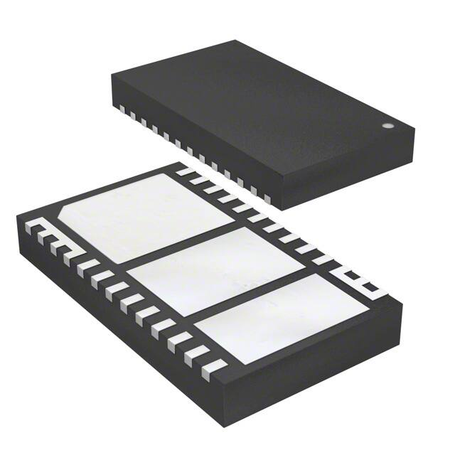
• Small 7mm x 4mm DFN Package
• U.S. Patent #6,922,041
SP7651
DFN PACKAGE
7mm x 4mm
LX
26
LX
25
LX
24
LX
23
BOTTOM VIEW
1
PGND
Heatsink Pad 1
Connect to Lx
2
PGND
3
PGND
Pin 27
VCC 22
GND
21
GND
20
GND
19
BST
Heatsink Pad 2
Connect to GND
4
GND
5
VFB
6
COMP
7
UVIN
8
GND
18
9
SS
NC
17
10
VIN
LX
16
11
VIN
LX
15
LX
14
Pin 28
Heatsink Pad 3
Connect to VIN
Pin 29
12
VIN
13
VIN
So
DESCRIPTION
The SP7651 is a high voltage synchronous step-down switching regulator optimized for high efficiency. The part
is designed to be especially attractive for dual supply, 12V step down with 5V used to power the controller. This
lower VCC voltage minimizes power dissipation in the part. The SP7651 is designed to provide a fully integrated
buck regulator solution using a fixed 900kHz frequency, PWM voltage mode architecture. Protection features
include UVLO, thermal shutdown and output short circuit protection. The SP7651 is available in the space saving
7mm X 4mm DFN package.
TYPICAL APPLICATION CIRCUIT
U�
SP7651
�
Rz2
Cz2
2
3
�,000pF �5k,1%
4
CP�
5
22pF
CF�
6
ENABLE
�00pF
7
8
9
CSS
�5nF
�0
��
�2
�3
VIN
12V
C�
Rev J: 3/14/07
LX
PGND
LX
PGND
LX
GND
LX
VFB
VCC
COMP
GND
UVIN
GND
GND
GND
SS
BST
VIN
NC
VIN
LX
VIN
LX
VIN
LX
L�
26
25
4.7uH, Irate=3.87A
+5V
VCC
24
23
22
2�
20
CVCC
DBST
�8
�6
�5
�4
C3
22uF
6.3V
7.�5kΩ,
1%
Cz3
VOUT
3.3V
0-3A
R�
68.�kΩ,�%
�50pF
2.2uF
�9
�7
Rz3
SD101AWS
CBST
RSET
2�.5kΩ,�%
(note 2)
6800pF
fs=900Khz
22uF
16V
GND
PGND
Notes:
1. U1 Bottom-Side Layout should
have three contacts isolated from
one another: Vin, SWNODE, and GND.
2. RSET=54.48/(Vout-0.8V) (KOhm)
SP7651 Wide Input Voltage Range 3A, 900kHz, Buck Regulator
�
© Copyright 2007 Sipex Corporation
�ABSOLUTE MAXIMUM RATINGS
These are stress ratings only and functional operation of the device at these ratings or any other above those indicated in the operation sections
of the specifications below is not implied. Exposure to absolute maximum rating conditions for extended periods of time may affect reliability.
All other pins.............................................................-0.3V to VCC+0.3V
VCC .................................................................................................. 7V
VIN.................................................................................................. 22V
ILX..................................................................................................... 5A
BST................................................................................................. 35V
LX-BST................................................................................-0.3V to 7V
LX.........................................................................................-1V to 20V
Storage Temperature.................................................... -65°C to 150°C
Power Dissipation...................................................... Internally Limited
ESD Rating............................................................................ 2kV HBM
Thermal Resistance ΟJC. .......................................................... 5°C/W
ELECTRICAL CHARACTERISTICS
Unless otherwise specified: -40°C < TAMB < 85°C, -40°C< Tj Rz3
Output Load Resistance >> R ESR & R
DC
Voltage Feedback
G FBK Gain Block
R2
V FBK
(Volts)
(R 1 + R 2 )
or
V REF
V OUT
SP7651 Voltage Mode Control Loop with Loop Dynamic
Definitions:
RESR = Output Capacitor Equivalent Series Resistance
RDC = Output Inductor DC Resistance
RRAMP_PP = SP7651 internal RAMP Amplitude Peak-to-Peak Voltage
Rev J: 3/14/07
SP7651 Wide Input Voltage Range 3A, 900kHz, Buck Regulator
�
© Copyright 2007 Sipex Corporation
�APPLICATIONS INFORMATION
Gain
(dB)
Error Amplifier Gain
Bandwidth Product
Condition:
C22 >> CP1, R1 >> RZ3
1/6.28(RZ3) (CZ3)
1/6.28(RZ2) (CP1)
1/6.28(R1) (CZ2)
1/6.28(R1) (CZ3)
1/6.28(R22) (CZ2)
20 Log (RZ2/R1)
Frequency
(Hz)
Bode Plot of Type III Error Amplifier Compensation.
CP1
RZ3
CZ3
CZ2
V OUT
R1
68.1k, 1%
5
VFB
R SET
+
+
- 0.8V
R SET
RZ2
6
COMP
CF1
=54.48/ (V OUT -0.8) (kΩ)
Type III Error Amplifier Compensation Circuit
Rev J: 3/14/07
SP7651 Wide Input Voltage Range 3A, 900kHz, Buck Regulator
10
© Copyright 2007 Sipex Corporation
�APPLICATIONS INFORMATION
data was taken for still air, not with
forced air. If forced air is used, some
improvement in thermal resistance
would be seen.
SP765X Thermal Resistance
The SP765X family has been tested with a
variety of footprint layouts along with different copper area and thermal resistance has
been measured. The layouts were done on
4 layer FR4 PCB with the top and bottom
layers using 3oz copper and the power and
ground layers using 1oz copper.
SP765X Thermal Resistance
For the Minimum footprint, only about 0.1
square inch of 3 ounces of copper was
used on the top or footprint layer, and this
layer had no vias to connect to the 3 other
layers. For the Medium footprint, about 0.7
square inches of 3 ounces of copper was
used on the top layer, but vias were used
to connect to the other 3 layers. For the
Maximum footprint, about 1.0 square inch
of 3 ounces of copper was used on the top
layer and many vias were used to connect
to the 3 other layers.
4 Layer Board:
Top Layer 3ounces Copper
GND Layer 1ounce Copper
Power Layer 1ounce Copper
Bottom Layer 3ounces Copper
The results show that only about 0.7 square
inches of 3 ounces of copper on the top
layer and vias connecting to the 3 other
layers are needed to get the best thermal
resistance of 36°C/W. Adding area on the
top beyond the 0.7 square inches did not
reduce thermal resistance.
Maximum Footprint: 36°C/W
Top Layer: 1.0 square inch
Vias to other 3 Layers
Minimum Footprint: 44°C/W
Top Layer: 0.1 square inch
No Vias to other 3 Layers
Medium Footprint: 36°C/W
Top Layer: 0.7 square inch
Vias to other 3 Layers
Using a minimum of 0.1 square inches of
(3 ounces of) Copper on the top layer with
no vias connecting to the 3 other layers
produced a thermal resistance of 44°C/W.
This thermal impedance is only 22% higher
than the medium and large footprint layouts,
indicating that space constrained designs
can still benefit thermally from the Powerblox
family of ICs. This indicates that a minimum
footprint of 0.1 square inch, if used on a
4 layer board, can produce 44°C/W thermal resistance. This approach is still very
worthwhile if used in a space constrained
design.
The following page shows the footprint
layouts from an ORCAD file. The thermal
Rev J: 3/14/07
SP7651 Wide Input Voltage Range 3A, 900kHz, Buck Regulator
11
© Copyright 2007 Sipex Corporation
�Rev J: 3/14/07
SP7651 Wide Input Voltage Range 3A, 900kHz, Buck Regulator
12
© Copyright 2007 Sipex Corporation
�TYPICAL PERFORMANCE CHARACTERISITICS
Rev J: 3/14/07
SP7651 Wide Input Voltage Range 3A, 900kHz, Buck Regulator
13
© Copyright 2007 Sipex Corporation
�Package: 26 Pin dfn
Rev J: 3/14/07
SP7651 Wide Input Voltage Range 3A, 900kHz, Buck Regulator
14
© Copyright 2007 Sipex Corporation
�ORDERING INFORMATION
Part Number
MIN. Temp. (°C)
MAX. Temp.(°C)
Status
SP7651ER
Package Code
DFN26
RoHS
-40
85
Active
Pack Quantity
Bulk
SP7651ER/TR
DFN26
-40
85
Active
500 Tape & Reel
SP7651ER-L
DFN26
▪
-40
85
Active
Bulk
SP7651ER-L/TR
DFN26
▪
-40
85
Active
500 Tape & Reel
Sipex Corporation
Headquarters and
Sales Office
233 South Hillview Drive
Milpitas, CA 95035
TEL: (408) 934-7500
FAX: (408) 935-7600
Sipex Corporation reserves the right to make changes to any products described herein. Sipex does not assume any liability arising out of the application or use of any product or circuit described herein; neither does it convey any license under its patent rights nor the rights of others.
Rev J: 3/14/07
SP7651 Wide Input Voltage Range 3A, 900kHz, Buck Regulator
15
© Copyright 2007 Sipex Corporation
�
很抱歉,暂时无法提供与“SP7651ER-L”相匹配的价格&库存,您可以联系我们找货
免费人工找货