XRP6657
1.5A 1.3MHz Synchronous Step Down Converter
November 2019
Rev. 1.5.1
GENERAL DESCRIPTION
APPLICATIONS
• Point of Loads
The XRP6657 is a high efficiency synchronous
step down DC to DC converter capable of
delivering up to 1.5 Amp of current and
optimized
for
portable
battery-operated
applications.
• Set-Top Boxes
• Portable Media Players
• Hard Disk Drives
Operating over an input voltage range of 2.5V
to 5.5V, it provides an adjustable regulated
output voltage down to 0.6V. The XRP6657
uses a constant 1.3 MHz frequency pulse width
modulation (PWM) scheme allowing for
compact external components, low output
voltage ripple and fixed frequency noise, while
Pulse Skip Mode (PSM) is used to improve
light load efficiency. A low dropout mode
provides 100% duty cycle operation.
FEATURES
• Guaranteed 1.5A Output Current
− Fixed 1.3MHz Frequency PWM Operations
− Up to 95% efficiency
− Input Voltage: 2.5V to 5.5V
• Adjustable Output Voltage
• Internal Compensation Network
The solution footprint is further reduced by a
current mode internal compensation network
and built-in synchronous switch removing the
need for an external Schottky. Over-current
and over-temperature protection insures safe
operations
under
abnormal
operating
conditions.
• No Schottky Diode Required
• LDO Operation: 100% Duty Cycle
• 240μA Quiescent Current (no load)
• 1μA Shutdown Current
• Soft Start Function
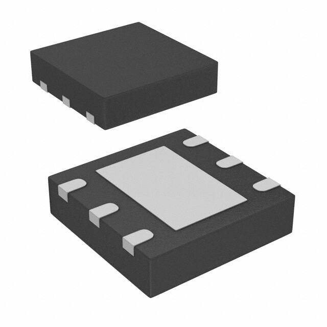
The XRP6657 is available in a compact RoHS
compliant “green”/halogen free thin 6-pin DFN
package.
• Over-current/Over-temperature
Protection
• “Green”/Halogen Free DFN-6 Package
TYPICAL APPLICATION DIAGRAM
Fig. 1: XRP6657 Application Diagram
1/12
Rev. 1.5.1
�XRP6657
1.5A 1.3MHz Synchronous Step Down Converter
ABSOLUTE MAXIMUM RATINGS
OPERATING RATINGS
These are stress ratings only and functional operation of
the device at these ratings or any other above those
indicated in the operation sections of the specifications
below is not implied. Exposure to absolute maximum
rating conditions for extended periods of time may affect
reliability.
Input Voltage Range VIN ............................... 2.5V to 5.5V
Ambient Temperature Range TA ................. -40°C to 85°C
Junction Temperature Range TJ.................-40°C to 125°C
Thermal Resistance θJC ...................................... 10°C/W
Thermal Resistance θJA ...................................... 55°C/W
Input Voltage VIN ....................................... -0.3V to 6.0V
EN, VFB Voltage ........................................... -0.3V to VIN
SW Voltage ...................................... -0.3V to (VIN+0.3V)
PMOS Switch Source Current (DC) .............................. 2A
NMOS Switch Sink Current (DC) ................................. 2A
Peak Switch Sink and Source Current....................... 3.5A
Lead Temperature (Soldering, 10 sec) ................... 260°C
Storage Temp. Range TSTG ....................... -65ºC to 150°C
ESD Rating (HBM - Human Body Model) .................... 2kV
ESD Rating (MM - Machine Model) ...........................200V
Note 1: TJ is a function of the ambient temperature TA and
power dissipation PD (TJ= TA + PD x 55°C/W).
Note 2:XRP6657 has a build-in temperature protection
circuitry to avoid damages from overload conditions.
ELECTRICAL SPECIFICATIONS
Specifications are for an Operating Junction Temperature of TA = 25°C only; limits applying over the full Operating Ambient
Temperature range are denoted by a “•”. Minimum and Maximum limits are guaranteed through test, design, or statistical
correlation. Typical values represent the most likely parametric norm at TA = 25°C, and are provided for reference purposes
only. Unless otherwise indicated, VIN = 5.0V, TA= 25°C.
Parameter
Min.
Typ.
Feedback Current IVFB
Regulated Feedback Voltage VFB
Output Over-Voltage Lockout
ΔVOVL
Units
nA
0.588
0.600
0.612
0.585
0.600
0.615
Reference Voltage Line
Regulation ΔVFB3
Output Voltage Accuracy ΔVOUT%
Max.
±100
-2.5
20
50
Output Voltage Line Regulation
ΔVOUT4
Peak Inductor Current IPK
V
VIN = 2.5V to 5.5V
2.5
%
•
80
mV
0.4
%/V
0.2
%/A
Quiescent Current IQ2
240
Minimum Duty Cycle DMIN
-40°C ≤ TA ≤ 85°C
•
Output Voltage Load Regulation
VLOADREG
1.04
•
%/V
A
Oscillator Frequency fOSC
TA = 25°C
0.4
2.4
Shutdown Current ISHTDWN
Conditions
340
ΔVOVL = VOVL - VFB
•
VIN=3V, VFB=0.5V or VOUT=90%,
duty cycle1.2V: Enables the XRP6657
很抱歉,暂时无法提供与“XRP6657IHBTR-F”相匹配的价格&库存,您可以联系我们找货
免费人工找货