xr
XRT75R03
THREE CHANNEL E3/DS3/STS-1 LINE INTERFACE UNIT WITH JITTER ATTENUATOR
MARCH 2006
REV. 1.0.8
GENERAL DESCRIPTION
TRANSMITTER:
The XRT75R03 is a three-channel fully integrated
Line Interface Unit (LIU) featuring EXAR’s R3
Technology (Reconfigurable, Relayless Redundancy)
with Jitter Attenuator for E3/DS3/STS-1 applications.
It
incorporates
3
independent
Receivers,
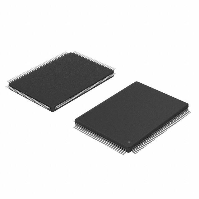
Transmitters and Jitter Attenuators in a single 128 pin
LQFP package.
Each channel of the XRT75R03 can be
independently configured to operate in the data rate,
E3 (34.368 MHz), DS3 (44.736 MHz) or STS-1 (51.84
MHz). Each transmitter can be turned off and tristated for redundancy support or for conserving
power.
The XRT75R03’s differential receiver provides high
noise interference margin and is able to receive the
data over 1000 feet of cable or with up to 12 dB of
cable attenuation.
The XRT75R03 incorporates an advanced crystalless jitter attenuator per channel that can be selected
either in the transmit or receive path. The jitter
attenuator performance meets the ETSI TBR-24 and
Bellcore GR-499 specifications.
The XRT75R03 provides both Serial Microprocessor
Interface as well as Hardware mode for programming
and control.
The XRT75R03 supports local, remote and digital
loop-backs. The device also has a built-in Pseudo
Random Binary Sequence (PRBS) generator and
detector with the ability to insert and detect single bit
error for diagnostic purposes.
FEATURES
RECEIVER:
• R3
Technology
Redundancy)
• R3
Technology
Redundancy)
(Reconfigurable,
Relayless
• Compliant with Bellcore GR-499, GR-253 and ANSI
T1.102 Specification for transmit pulse
• Tri-state Transmit output capability for redundancy
applications
• Each Transmitter can be independently turned on
or off
• Transmitters provide Voltage Output Drive
JITTER ATTENUATOR:
• On chip advanced crystal-less Jitter Attenuator for
each channel
• Jitter Attenuator can be selected in Receive or
Transmit paths
• Meets ETSI TBR 24 Jitter Transfer Requirements
• Compliant with jitter transfer template outlined in
ITU G.751, G.752, G.755 and GR-499-CORE,1995
standards
• 16 or 32 bits selectable FIFO size
• Jitter Attenuator can be disabled
CONTROL AND DIAGNOSTICS:
• 5 wire Serial Microprocessor Interface for control
and configuration
• Supports
optional
internal
Transmit
• Hardware Mode for control and configuration
• Each channel supports Local, Remote and Digital
Loop-backs
(Reconfigurable,
Relayless
• On chip Clock and Data Recovery circuit for high
input jitter tolerance
• Meets E3/DS3/STS-1 Jitter Tolerance Requirement
• Detects and Clears LOS as per G.775
• Receiver Monitor mode handles up to 20 dB flat
loss with 6 dB cable attenuation
• On chip B3ZS/HDB3 encoder and decoder that can
be either enabled or disabled
• On-chip clock synthesizer provides the appropriate
rate clock from a single 12.288 MHz Clock
• Provides low jitter output clock
driver
monitoring
• Single 3.3 V ± 5% power supply
• 5 V Tolerant digital inputs
• Available in 128 pin LQFP
• - 40°C to 85°C Industrial Temperature Range
APPLICATIONS
• E3/DS3 Access Equipment
• DSLAMs
• Digital Cross Connect Systems
• CSU/DSU Equipment
• Routers
• Fiber Optic Terminals
Exar Corporation 48720 Kato Road, Fremont CA, 94538 • (510) 668-7000 • FAX (510) 668-7017 • www.exar.com
�xr
XRT75R03
THREE CHANNEL E3/DS3/STS-1 LINE INTERFACE UNIT WITH JITTER ATTENUATOR
REV. 1.0.8
FIGURE 1. BLOCK DIAGRAM OF THE XRT 75R03
SDI
SDO
INT
SClk
CS
RESET
HOST/HW
STS-1/DS3_(n)
E3_(n)
REQEN_(n)
RTIP_(n)
RRing_(n)
SR/DR
LLB_(n)
XRT75R03
XRT75R03
Serial
Processor
Interface
CLKOUT
E3Clk,DS3Clk,
STS-1Clk
RLOL_(n)
RxON
RxClkINV
Clock
Synthesizer
Peak Detector
AGC/
Equalizer
Clock & Data
Recovery
Slicer
Jitter
Attenuator
LOS
Detector
Local
LoopBack
MUX
Invert
RxClk_(n)
HDB3/
B3ZS
Decoder
RPOS_(n)
Remote
LoopBack
RNEG_(n)/
LCV_(n)
RLB_(n)
RLOS_(n)
LOSTHR
JATx/Rx
TTIP_(n)
TRing_(n)
MTIP_(n)
MRing_(n)
Line
Driver
Device
Monitor
Tx
Pulse
Shaping
Jitter
Attenuator
Timing
Control
MUX
HDB3/
B3ZS
Encoder
TPData_(n)
TNData_(n)
TxClk_(n)
TAOS_(n)
Tx
Control
DMO_(n)
TxLEV_(n)
Channel 0
TxON_(n)
Channel 1
Channel 2
Notes: 1. (n) = 0, 1 or 2 for respective Channels
2. Serial Processor Interface input pins are shared by the three Channels in "Host" Mode and redefined in the "Hardware" Mode.
TRANSMIT INTERFACE CHARACTERISTICS
• Accepts either Single-Rail or Dual-Rail data from Terminal Equipment and generates a bipolar signal to the
line
• Integrated Pulse Shaping Circuit
• Built-in B3ZS/HDB3 Encoder (which can be disabled)
• Accepts Transmit Clock with duty cycle of 30%-70%
• Generates pulses that comply with the ITU-T G.703 pulse template for E3 applications
• Generates pulses that comply with the DSX-3 pulse template, as specified in Bellcore GR-499-CORE and
ANSI T1.102_1993
• Generates pulses that comply with the STSX-1 pulse template, as specified in Bellcore GR-253-CORE
• Transmitter can be turned off in order to support redundancy designs
RECEIVE INTERFACE CHARACTERISTICS
• Integrated Adaptive Receive Equalization (optional) for optimal Clock and Data Recovery
• Declares and Clears the LOS defect per ITU-T G.775 requirements for E3 and DS3 applications
• Meets Jitter Tolerance Requirements, as specified in ITU-T G.823_1993 for E3 Applications
• Meets Jitter Tolerance Requirements, as specified in Bellcore GR-499-CORE for DS3 Applications
• Declares Loss of Signal (LOS) and Loss of Lock (LOL) Alarms
• Built-in B3ZS/HDB3 Decoder (which can be disabled)
• Recovered Data can be muted while the LOS Condition is declared
• Outputs either Single-Rail or Dual-Rail data to the Terminal Equipment
2
�xr
XRT75R03
THREE CHANNEL E3/DS3/STS-1 LINE INTERFACE UNIT WITH JITTER ATTENUATOR
REV. 1.0.8
102
101
100
99
98
97
96
95
94
93
92
91
90
89
88
87
86
85
84
83
82
81
80
79
78
77
76
75
74
73
72
71
70
69
68
67
66
65
TEST
RESET
AGND_2
LOSTHR
STS-1/DS3_1
LLB_1
RLB_1
REQEN_1
E3_1
RxAVDD_1
RRing_1
RTIP_1
RxAGND_1
RxAGND_2
RTIP_2
RRing_2
RxAVDD_2
E3_2
REQEN_2
RLB_2
LLB_2
STS-1/DS3_2
RxAGND_0
RTIP_0
RRing_0
RxAVDD_0
E3_0
REQEN_0
RLB_0
LLB_0
STS-1/DS3_0
LOSMUT/INT
HOST/HW
RxMON/SDO
RxON/SDI
TxClkINV/SClk
RxClkINV/CS
SR/DR
FIGURE 2. PIN OUT OF THE XRT75R03
103
104
105
106
107
108
109
110
111
112
113
114
115
116
117
118
119
120
121
122
123
124
125
126
127
128
64
63
62
61
60
59
58
57
56
55
54
53
52
51
50
49
48
47
46
45
44
43
42
41
40
39
XRT75R03
RLOL_2
RLOS_2
ICT
RLOL_0
RLOS_0
RxDGND_0
RPOS_0
RNEG_0/LCV_0
RxClk_0
RxDVDD_0
RxDVDD_2
RPOS_2
RNEG_2/LCV_2
RxClk_2
RxDGND_2
AGND_0
JAGND_2
JAGND_0
JAVDD_0
JAVDD_2
JA0
JATx/Rx
JA1
TxAGND_0
DMO_0
TxAVDD_0
TxON_1
TNData_1
TPData_1
TxClk_1
MRing_1
MTIP_1
TAOS_1
TAOS_2
TxLEV_1
TxLEV_2
TTIP_1
TxVDD_1
TRing_1
TxGND_1
TxAGND_2
MRing_2
MTIP_2
TxGND_2
TRing_2
TxVDD_2
TTIP_2
DMO_2
TxAVDD_2
TNData_2
TPData_2
TxClk_2
TxGND_0
TRing_0
TxVDD_0
TTIP_0
MTIP_0
MRing_0
TNData_0
TPData_0
TxClk_0
TxLEV_0
TAOS_0
TxON_0
1
2
3
4
5
6
7
8
9
10
11
12
13
14
15
16
17
18
19
20
21
22
23
24
25
26
27
28
29
30
31
32
33
34
35
36
37
38
RLOL_1
RLOS_1
EXDGND
SFM_EN
E3Clk/CLK_EN
DS3Clk/CLK_OUT
STS-1Clk/12M
EXDVDD
RxDVDD_1
RPOS_1
RNEG_1/LCV_1
RxClk_1
RxDGND_1
AGND_1
JADGND
JAGND_1
JADVDD
JAVDD_1
REFAVDD
RXA
RXB
REFGND
TxON_2
TxAGND_1
DMO_1
TxAVDD_1
ORDERING INFORMATION
PART NUMBER
PACKAGE
OPERATING TEMPERATURE RANGE
XRT75R03IV
128 Pin LQFP
- 40°C to + 85°C
3
�xr
XRT75R03
REV. 1.0.8
THREE CHANNEL E3/DS3/STS-1 LINE INTERFACE UNIT WITH JITTER ATTENUATOR
GENERAL DESCRIPTION .................................................................................................1
FEATURES .........................................................................................................................1
APPLICATIONS ................................................................................................................................................1
FIGURE 1. BLOCK DIAGRAM OF THE XRT 75R03.............................................................................................................................. 2
TRANSMIT INTERFACE CHARACTERISTICS ........................................................................................................2
RECEIVE INTERFACE CHARACTERISTICS ..........................................................................................................2
FIGURE 2. PIN OUT OF THE XRT75R03 ........................................................................................................................................... 3
ORDERING INFORMATION.....................................................................................................................3
PIN DESCRIPTIONS (BY FUNCTION) ..............................................................................4
SYSTEM-SIDE TRANSMIT INPUT AND TRANSMIT CONTROL PINS .......................................................................4
TRANSMIT LINE SIDE PINS ..............................................................................................................................8
SYSTEM-SIDE RECEIVE OUTPUT AND RECEIVE CONTROL PINS ......................................................................10
RECEIVE LINE SIDE PINS ..............................................................................................................................17
GENERAL CONTROL PINS .............................................................................................................................18
CONTROL AND ALARM INTERFACE .................................................................................................................20
JITTER ATTENUATOR INTERFACE ...................................................................................................................20
POWER SUPPLY AND GROUND PINS .............................................................................................................22
XRT75R03 PIN LISTING IN NUMERICAL ORDER ............................................................................................24
1.0 R3 TECHNOLOGY (RECONFIGURABLE, RELAYLESS REDUNDANCY) ........................................29
1.1 NETWORK ARCHITECTURE ......................................................................................................................... 29
FIGURE 3. NETWORK REDUNDANCY ARCHITECTURE ...................................................................................................................... 29
1.2 POWER FAILURE PROTECTION .................................................................................................................. 29
1.3 SOFTWARE VS HARDWARE AUTOMATIC PROTECTION SWITCHING ................................................... 29
2.0 ELECTRICAL CHARACTERISTICS ....................................................................................................30
TABLE 1: ABSOLUTE MAXIMUM RATINGS ......................................................................................................................................... 30
TABLE 2: DC ELECTRICAL CHARACTERISTICS: ................................................................................................................................ 30
3.0 TIMING CHARACTERISTICS ..............................................................................................................31
FIGURE 4.
FIGURE 5.
FIGURE 6.
FIGURE 7.
TYPICAL INTERFACE BETWEEN TERMINAL EQUIPMENT AND THE XRT75R03 (DUAL-RAIL DATA) .......................................... 31
TRANSMITTER TERMINAL INPUT TIMING .......................................................................................................................... 31
RECEIVER DATA OUTPUT AND CODE VIOLATION TIMING ................................................................................................... 32
TRANSMIT PULSE AMPLITUDE TEST CIRCUIT FOR E3, DS3 AND STS-1 RATES ................................................................. 32
4.0 LINE SIDE CHARACTERISTICS: ........................................................................................................33
4.1 E3 LINE SIDE PARAMETERS: ...................................................................................................................... 33
FIGURE 8. PULSE MASK FOR E3 (34.368 MBITS/S) INTERFACE AS PER ITU-T G.703......................................................................... 33
TABLE 3: E3 TRANSMITTER LINE SIDE OUTPUT AND RECEIVER LINE SIDE INPUT SPECIFICATIONS........................................................ 34
FIGURE 9. BELLCORE GR-253 CORE TRANSMIT OUTPUT PULSE TEMPLATE FOR SONET STS-1 APPLICATIONS............................. 35
TABLE 4: STS-1 PULSE MASK EQUATIONS ..................................................................................................................................... 35
TABLE 5: STS-1 TRANSMITTER LINE SIDE OUTPUT AND RECEIVER LINE SIDE INPUT SPECIFICATIONS (GR-253) .............................. 36
FIGURE 10. TRANSMIT OUPUT PULSE TEMPLATE FOR DS3 AS PER BELLCORE GR-499 ................................................................... 37
TABLE 6: DS3 PULSE MASK EQUATIONS ........................................................................................................................................ 37
TABLE 7: DS3 TRANSMITTER LINE SIDE OUTPUT AND RECEIVER LINE SIDE INPUT SPECIFICATIONS (GR-499) ................................. 38
FIGURE 11. MICROPROCESSOR SERIAL INTERFACE STRUCTURE...................................................................................................... 38
FIGURE 12. TIMING DIAGRAM FOR THE MICROPROCESSOR SERIAL INTERFACE ................................................................................ 39
TABLE 8: MICROPROCESSOR SERIAL INTERFACE TIMINGS ( TA = 250C, VDD=3.3V± 5% AND LOAD = 10PF) .................................. 39
FUNCTIONAL DESCRIPTION: ........................................................................................40
5.0 THE TRANSMITTER SECTION: ..........................................................................................................40
FIGURE 13. SINGLE-RAIL OR NRZ DATA FORMAT (ENCODER AND DECODER ARE ENABLED)............................................................ 40
FIGURE 14. DUAL-RAIL DATA FORMAT (ENCODER AND DECODER ARE DISABLED) ............................................................................. 40
5.1 TRANSMIT CLOCK: ....................................................................................................................................... 41
5.2 B3ZS/HDB3 ENCODER: ................................................................................................................................. 41
5.2.1 B3ZS ENCODING: ...................................................................................................................................................... 41
FIGURE 15. B3ZS ENCODING FORMAT ........................................................................................................................................... 41
5.2.2 HDB3 ENCODING:...................................................................................................................................................... 41
FIGURE 16. HDB3 ENCODING FORMAT .......................................................................................................................................... 41
5.3 TRANSMIT PULSE SHAPER: ........................................................................................................................ 42
5.3.1 GUIDELINES FOR USING TRANSMIT BUILD OUT CIRCUIT: ................................................................................. 42
5.3.2 INTERFACING TO THE LINE: .................................................................................................................................... 42
5.4 TRANSMIT DRIVE MONITOR: ....................................................................................................................... 43
FIGURE 17. TRANSMIT DRIVER MONITOR SET-UP. ........................................................................................................................... 43
5.5 TRANSMITTER SECTION ON/OFF: .............................................................................................................. 43
I
�xr
XRT75R03
THREE CHANNEL E3/DS3/STS-1 LINE INTERFACE UNIT WITH JITTER ATTENUATOR
REV. 1.0.8
6.0 THE RECEIVER SECTION: ................................................................................................................. 43
6.1 AGC/EQUALIZER: .......................................................................................................................................... 43
6.1.1 INTERFERENCE TOLERANCE: ................................................................................................................................ 44
FIGURE 18. INTERFERENCE MARGIN TEST SET UP FOR DS3/STS-1................................................................................................ 44
FIGURE 19. INTERFERENCE MARGIN TEST SET UP FOR E3. ............................................................................................................ 45
TABLE 9: INTERFERENCE MARGIN TEST RESULTS ........................................................................................................................... 45
6.2 CLOCK AND DATA RECOVERY: .................................................................................................................. 45
6.3 B3ZS/HDB3 DECODER: ................................................................................................................................ 46
6.4 LOS (LOSS OF SIGNAL) DETECTOR: ......................................................................................................... 46
6.4.1 DS3/STS-1 LOS CONDITION: .................................................................................................................................... 46
TABLE 10: THE ALOS (ANALOG LOS) DECLARATION AND CLEARANCE THRESHOLDS FOR A GIVEN SETTING OF LOSTHR AND REQEN (DS3
AND STS-1 APPLICATIONS)............................................................................................................................................. 46
DISABLING ALOS/DLOS DETECTION: .......................................................................................................... 46
6.4.2 E3 LOS CONDITION:.................................................................................................................................................. 46
FIGURE 20. LOSS OF SIGNAL DEFINITION FOR E3 AS PER ITU-T G.775.......................................................................................... 47
FIGURE 21. LOSS OF SIGNAL DEFINITION FOR E3 AS PER ITU-T G.775. ......................................................................................... 47
6.4.3 MUTING THE RECOVERED DATA WITH LOS CONDITION:................................................................................... 48
7.0 JITTER: ................................................................................................................................................ 48
7.1 JITTER TOLERANCE - RECEIVER: .............................................................................................................. 48
FIGURE 22. JITTER TOLERANCE MEASUREMENTS ........................................................................................................................... 48
7.1.1 DS3/STS-1 JITTER TOLERANCE REQUIREMENTS:............................................................................................... 48
FIGURE 23. INPUT JITTER TOLERANCE FOR DS3/STS-1................................................................................................................ 49
7.1.2 E3 JITTER TOLERANCE REQUIREMENTS:............................................................................................................. 49
FIGURE 24. INPUT JITTER TOLERANCE FOR E3 .............................................................................................................................. 49
TABLE 11: JITTER AMPLITUDE VERSUS MODULATION FREQUENCY (JITTER TOLERANCE) .................................................................. 50
7.2 JITTER TRANSFER - RECEIVER/TRANSMITTER: ...................................................................................... 50
TABLE 12: JITTER TRANSFER SPECIFICATION/REFERENCES ............................................................................................................ 50
7.3 JITTER ATTENUATOR: ................................................................................................................................. 50
TABLE 13: JITTER TRANSFER PASS MASKS .................................................................................................................................... 51
FIGURE 25. JITTER TRANSFER REQUIREMENTS AND JITTER ATTENUATOR PERFORMANCE ................................................................ 51
7.3.1 JITTER GENERATION: .............................................................................................................................................. 51
8.0 SERIAL HOST INTERFACE: ............................................................................................................... 51
TABLE 14: FUNCTIONS OF SHARED PINS ......................................................................................................................................... 52
TABLE 15: XRT75R03 REGISTER MAP - QUICK LOOK .................................................................................................................... 53
Legend: ..................................................................................................................................................................... 56
THE REGISTER MAP AND DESCRIPTION FOR THE XRT75R03 3-CHANNEL DS3/E3/STS-1 LIU IC 56
TABLE 16: COMMAND REGISTER ADDRESS MAP, WITHIN THE XRT75R03 3-CHANNEL DS3/E3/STS-1 LIU W/ JITTER ATTENUATOR IC56
THE GLOBAL/CHIP-LEVEL REGISTERS ................................................................................................ 58
TABLE 17: LIST AND ADDRESS LOCATIONS OF GLOBAL REGISTERS ................................................................................................. 58
REGISTER DESCRIPTION - GLOBAL REGISTERS ............................................................................... 58
TABLE 18:
TABLE 19:
TABLE 20:
TABLE 21:
TABLE 22:
APS/REDUNDANCY CONTROL REGISTER - CR0 (ADDRESS LOCATION = 0X00) ............................................................... 58
BLOCK LEVEL INTERRUPT ENABLE REGISTER - CR32 (ADDRESS LOCATION = 0X20)....................................................... 61
BLOCK LEVEL INTERRUPT STATUS REGISTER - CR33 (ADDRESS LOCATION = 0X21)....................................................... 62
DEVICE/PART NUMBER REGISTER - CR62 (ADDRESS LOCATION = 0X3E) ....................................................................... 63
CHIP REVISION NUMBER REGISTER - CR63 (ADDRESS LOCATION = 0X3F)..................................................................... 64
THE PER-CHANNEL REGISTERS ........................................................................................................... 64
TABLE 23: COMMAND REGISTER ADDRESS MAP, WITHIN THE XRT75R03 3-CHANNEL DS3/E3/STS-1 LIU W/ JITTER ATTENUATOR IC64
REGISTER DESCRIPTION - PER CHANNEL REGISTERS .................................................................... 66
TABLE 24:
TABLE 25:
TABLE 26:
TABLE 27:
TABLE 28:
TABLE 29:
TABLE 30:
SOURCE LEVEL INTERRUPT ENABLE REGISTER - CHANNEL 0 ADDRESS LOCATION = 0X01 .............................................. 66
SOURCE LEVEL INTERRUPT STATUS REGISTER - CHANNEL 0 ADDRESS LOCATION = 0X02 .............................................. 68
ALARM STATUS REGISTER - CHANNEL 0 ADDRESS LOCATION = 0X03............................................................................. 70
TRANSMIT CONTROL REGISTER - CHANNEL 0 ADDRESS LOCATION = 0X04 ..................................................................... 75
RECEIVE CONTROL REGISTER - CHANNEL 0 ADDRESS LOCATION = 0X05 ....................................................................... 78
CHANNEL CONTROL REGISTER - CHANNEL 0 ADDRESS LOCATION = 0X06 ...................................................................... 80
JITTER ATTENUATOR CONTROL REGISTER - CHANNEL 0 ADDRESS LOCATION = 0X07 ..................................................... 83
9.0 DIAGNOSTIC FEATURES: ................................................................................................................. 84
9.1 PRBS GENERATOR AND DETECTOR: ........................................................................................................ 84
FIGURE 26. PRBS MODE ............................................................................................................................................................. 84
9.2 LOOPBACKS: ................................................................................................................................................ 84
9.2.1 ANALOG LOOPBACK:............................................................................................................................................... 84
FIGURE 27. ANALOG LOOPBACK ..................................................................................................................................................... 85
9.2.2 DIGITAL LOOPBACK:................................................................................................................................................ 86
FIGURE 28. DIGITAL LOOPBACK...................................................................................................................................................... 86
II
�xr
XRT75R03
REV. 1.0.8
THREE CHANNEL E3/DS3/STS-1 LINE INTERFACE UNIT WITH JITTER ATTENUATOR
9.2.3 REMOTE LOOPBACK:............................................................................................................................................... 86
FIGURE 29. REMOTE LOOPBACK .................................................................................................................................................... 86
9.3 TRANSMIT ALL ONES (TAOS): .................................................................................................................... 87
FIGURE 30. TRANSMIT ALL ONES (TAOS) ...................................................................................................................................... 87
ORDERING INFORMATION.............................................................................................88
PACKAGE DIMENSIONS - 14X20 MM, 128 PIN PACKAGE .................................................................................88
REVISIONS ...................................................................................................................................................89
III
�xr
XRT75R03
THREE CHANNEL E3/DS3/STS-1 LINE INTERFACE UNIT WITH JITTER ATTENUATOR
REV. 1.0.8
PIN DESCRIPTIONS (BY FUNCTION)
SYSTEM-SIDE TRANSMIT INPUT AND TRANSMIT CONTROL PINS
PIN #
SIGNAL NAME
TYPE
38
1
125
TxON_0
TxON_1
TxON_2
I
DESCRIPTION
Transmitter ON Input - Channel 0:
Transmitter ON Input - Channel 1:
Transmitter ON Input - Channel 2:
These input pins are used to either enable or disable the Transmit Output
Driver corresponding to Channel_n.
"Low" - Disables the Transmit Output Driver of the corresponding Channel.
In this setting, the corresponding TTIP_n and TRING_n output pins will be
tri-stated.
"High" - Enables the Transmit Output Driver of the corresponding Channel.
In this setting, the corresponding TTIP_n and TRING_n output pins will be
enabled.
NOTES:
35
4
26
TxClk_0
TxClk_1
TxClk_2
I
1.
Even when the XRT75R03 is configured in HOST mode, these
pins will be active. To enable software control of the Transmit
Output Driver outputs, pull these pins "High".
2.
When Transmitters are turned off either in Host or Hardware
mode, the TTIP and TRing outputs are Tri-stated.
3.
These pins are internally pulled "High"
Transmit Clock Input - Channel 0:
Transmit Clock Input f - Channel 1:
Transmit Clock Input - Channel 2:
These input pins have two functions:
• They function as the timing source for the Transmit Section of the
corresponding channel within the XRT75R03.
• They also are used by the Transmit Section of the LIU IC to sample the
corresponding TPDATA_n and TNDATA_n input pin.
NOTE: The user is expected to supply a 44.736MHz ± 20ppm clock signal
(for DS3 applications), 34.368MHz ± 20 ppm clock signal (for E3
applications) or a 51.84MHz ± 4.6ppm clock signal (for STS-1,
Stratum 3E or better applications).
4
�xr
XRT75R03
REV. 1.0.8
THREE CHANNEL E3/DS3/STS-1 LINE INTERFACE UNIT WITH JITTER ATTENUATOR
SYSTEM-SIDE TRANSMIT INPUT AND TRANSMIT CONTROL PINS
PIN #
SIGNAL NAME
TYPE
34
3
25
TPDATA_0/TxDATA_0
TPDATA_1/TxDATA_1
TPDATA_2/TxDATA_2
I
DESCRIPTION
Transmit Positive Data Input - Channel 0:
Transmit Positive Data Input - Channel 1:
Transmit Positive Data Input - Channel 2:
Transmit Positive Data/Data Input - Channel n:
The function of these input pins depends upon whether the corresponding
channel has been configured to operate in the Single-Rail or Dual-Rail
Mode.
Single Rail Mode - Transmit Data Input - Channel n:
If the Channel has been configured to operate in the Single-Rail Mode,
then all transmit output data will be serially applied to this input pin. This
signal will latched into the Transmit Section circuitry upon either the rising
or falling edge of the TxCLK_n signal, depending upon user configuration.
In the Single-Rail Mode, the Transmit Section of the LIU IC will then encode
this data into either the B3ZS line code (for DS3 and STS-1 applications) or
the HDB3 line code (for E3 applications).
Dual Rail Mode - Transmit Positive Data Input - Channel n:
If the Channel has been configured to operate in the Dual-Rail Mode, then
the user should apply a pulse to this input pin, anytime the Transmit Section of the LIU IC is suppose to generate and transmit a positive-polarity
pulse onto the line. This signal will be latched into the Transmit Section circuitry upon either the rising or falling edge of the TxCLK_n signal, depending upon user configuration.
In the Dual-Rail Mode, the Transmit Section of the LIU IC will NOT encode
this data into either the B3ZS or HDB3 line codes. If the user configures
the LIU IC to operate in the Dual-Rail Mode, then B3ZS/HDB3 encoding
must have already been done prior to providing the transmit output data to
this input pin.
33
2
24
TNData_0
TNData_1
TNData_2
I
Transmit Negative Data Input - Channel 0:
Transmit Negative Data Input - Channel 1:
Transmit Negative Data Input - Channel 2:
If a Channel has been configured to operate in the Dual-Rail Mode, then
the user should apply a pulse to this input pin anytime the Transmit Section
of the LIU IC is suppose to generate and transmit a negative-polarity pulse
onto the line. This signal will be latched into the Transmit Section circuitry
upon either the rising or falling edge of the TxCLK_n signal, depending
upon user configuration.
NOTE: If the Channel has been configured operate in the Single-Rail Mode,
then this input pin has no function, and should be tied to GND.
5
�xr
XRT75R03
THREE CHANNEL E3/DS3/STS-1 LINE INTERFACE UNIT WITH JITTER ATTENUATOR
REV. 1.0.8
SYSTEM-SIDE TRANSMIT INPUT AND TRANSMIT CONTROL PINS
PIN #
SIGNAL NAME
TYPE
37
7
8
TAOS_0
TAOS_1
TAOS_2
I
DESCRIPTION
Transmit "All Ones" Input - Channel 0:
Transmit "All Ones" Input - Channel 1:
Transmit "All Ones" Input - Channel 2:
These input pin are used to configure the Transmit Section of the corresponding channel to generate and transmit an unframed "All Ones" pattern
via the DS3, E3 or STS-1 line signal to the remote terminal equipment.
When this configuration is implemented the Transmit Section will ignore the
data that it is accepting from the System-side equipment and will overwrite
this data will the "All Ones" Pattern.
"Low" - Does not configure the channel to transmit an unframed "All Ones"
Pattern to the remote terminal equipment. In this mode, the Transmit Section of the Channel will output data based upon the signals that are applied
to the TxPOS_n and TxNEG_n input pins.
"High" - Configures the Channel to transmit an unframed "All Ones" Pattern
to the remote terminal equipment. In this mode, the Transmit Section will
override the data that is applied to the TxPOS_n and TxNEG_n input pins,
and will proceed to generate and transmit an unframed "All Ones" pattern.
NOTES:
36
9
10
TxLEV_0
TxLEV_1
TxLEV_2
I
1.
This input pin is ignored if the XRT75R03 is operating in the
HOST Mode and should be tied to GND.
2.
These input pins are internally pulled down.
Transmit Line Build-Out Enable/Disable Select - Channel 0:
Transmit Line Build-Out Enable/Disable Select - Channel 1:
Transmit Line Build-Out Enable/Disable Select - Channel 2:
These input pins are used to enable or disable the Transmit Line Build-Out
(e.g., pulse-shaping) circuit within the corresponding channel. The user
should set these input pins either "High" or "Low" based upon the following
guidelines.
"Low" - If the cable length between the Transmit Output of the corresponding Channel and the DSX-3/STSX-1 location is 225 feet or less.
"High" - If the cable length between the Transmit Output of the corresponding Channel and the DSX-3/STSX-1 location is 225 feet or more.
NOTES:
1.
These guidelines must be followed in order to insure that the
Transmit Section of Channel_n will always generate a DS3 pulse
that complies with the Isolated Pulse Template requirements per
Bellcore GR-499-CORE, or an STS-1 pulse that complies with the
Pulse Template requirements per Telcordia GR-253-CORE.
2.
This input pin is inactive if the XRT75R03 has been configured to
operate in the Host Mode, or if the corresponding channel has
been configured to operate in the E3 Mode. If either of these
cases are true, then tie this input pin to GND.
3.
These input pins are internally pulled "Low".
6
�xr
XRT75R03
REV. 1.0.8
THREE CHANNEL E3/DS3/STS-1 LINE INTERFACE UNIT WITH JITTER ATTENUATOR
SYSTEM-SIDE TRANSMIT INPUT AND TRANSMIT CONTROL PINS
PIN #
SIGNAL NAME
TYPE
40
127
22
DMO_0
DMO_1
DMO_2
O
DESCRIPTION
Drive Monitor Output - Channel 0:
Drive Monitor Output - Channel 1:
Drive Monitor Output - Channel 2:
These output signals are used to indicate some sort of fault condition within
the Transmit Output signal path.
This output pin will toggle "High" anytime the Transmit Drive Monitor circuitry either, via the corresponding MTIP and MRING input pins or internally, detects no bipolar pulses via the Transmit Output line signal (e.g., via
the TTIP_n and TRING_n output pins) for 128 bit-periods.
This output pin will be driven "Low" anytime the Transmit Drive Monitor circuitry has detected at least one bipolar pulse via the Transmit Output line
signal within the last 128 bit periods.
67
TxClkINV/
SClk
I
Hardware Mode: Transmit Clock Invert
Host Mode: Serial Clock Input:
Hardware mode
This input pin is used to select the edge of the TxCLK_n input that the
Transmit Section of all channels will use to sample the TPDATA_n and
TNDATA_n input pins.
Setting this input pin “High” configures all three Transmitters to sample the
TPData_n and TNData_n data on the rising edge of the TxClk_n .
Setting this input pin “Low” configures all three Transmitters to sample the
TPData_n and TNData_n data on the falling edge of the TxClk_n .
Host Mode
In the Host Mode this pin functions as SClk input pin please refer to the pin
descriptions for the Microprocessor interface.
7
�xr
XRT75R03
THREE CHANNEL E3/DS3/STS-1 LINE INTERFACE UNIT WITH JITTER ATTENUATOR
REV. 1.0.8
TRANSMIT LINE SIDE PINS
PIN #
SIGNAL NAME
TYPE
30
11
21
TTIP_0
TTIP_1
TTIP_2
O
DESCRIPTION
Transmit TTIP Output - Positive Polarity Signal - Channel 0:
Transmit TTIP Output - Positive Polarity Signal - Channel 1:
Transmit TTIP Output - Positive Polarity Signal - Channel 2:
These output pins along with the corresponding TRING_n output pins, function
as the Transmit DS3/E3/STS-1 Line output signal drivers for a given channel, of
the XRT75R03.
Connect this signal and the corresponding TRING_n output signal to a 1:1
transformer.
Whenever the Transmit Section of the Channel generates and transmits a positive-polarity pulse onto the line, this output pin will be pulsed to a "higher-voltage" than its corresponding TRING_n output pins.
Conversely, whenever the Transmit Section of the Channel generates and
transmit a negative-polarity pulse onto the line, this output pin will be pulsed to a
"lower-voltage" than its corresponding TRING_n output pin.
NOTE: This output pin will be tri-stated whenever the corresponding TxON_n
input pin or bit-field is set to "0".
28
13
19
TRing_0
TRing_1
TRing_2
O
Transmit Ring Output - Negative Polarity Signal - Channel 0:
Transmit Ring Output - Negative Polarity Signal - Channel 1:
Transmit Ring Output - Negative Polarity Signal - Channel 2:
These output pins along with the corresponding TTIP_n output pins, function as
the Transmit DS3/E3/STS-1 Line output signal drivers for a given channel,
within the XRT75R03.
Connect this signal and the corresponding TTIP_n output signal to a 1:1 transformer.
Whenever the Transmit Section of the Channel generates and transmits a positive-polarity pulse onto the line. This output pin will be pulsed to a "lower-voltage" than its corresponding TTIP_n output pins.
Conversely, whenever the Transmit Section of the Channel generates and
transmit a negative-polarity pulse onto the line. This output pin will be pulsed to
a "higher-voltage" than its corresponding TTIP_n output pin.
NOTE: This output pin will be tri-stated whenever the corresponding TxON_n
input pin or bit-field is set to "0".
8
�xr
XRT75R03
REV. 1.0.8
THREE CHANNEL E3/DS3/STS-1 LINE INTERFACE UNIT WITH JITTER ATTENUATOR
TRANSMIT LINE SIDE PINS
PIN #
SIGNAL NAME
TYPE
31
6
17
MTIP_0
MTIP_1
MTIP_2
I
DESCRIPTION
Monitor Tip Input - Positive Polarity Signal - Channel 0:
Monitor Tip Input - Positive Polarity Signal - Channel 1:
Monitor Tip Input - Positive Polarity Signal - Channel 2:
These input pins along with MRING_n function as the Transmit Drive Monitor
Output (DMO) input monitoring pins. To (1) monitor the Transmit Output line
signal and (2) to perform this monitoring externally, then this pin MUST be connected to the corresponding TTIP_n output pin via a 274 ohm series resistor.
Similarly, the MRING_n input pin MUST also be connected to its corresponding
TRING_n output pin via a 274 ohm series resistor.
The MTIP_n and MRING_n input pins will continuously monitor the Transmit
Output line signal via the TTIP_n and TRING_n output pins for bipolar activity.
If these pins do not detect any bipolar activity for 128 bit periods, then the
Transmit Drive Monitor circuit will drive the corresponding DMO_n output pin
"High" in order to denote a possible fault condition in the Transmit Output Line
signal path.
NOTES:
32
5
16
MRing_0
MRing_1
MRing_2
I
1.
These input pins are inactive if the user choose to internally monitor
the Transmit Output line signal.
2.
Internal Monitoring is only available as an option if the XRT75R03 in is
being operated in the Host Mode.
Monitor Ring Input - Channel 0:
Monitor Ring Input - Channel 1:
Monitor Ring Input - Channel 2:
These input pins along with MTIP_n function as the Transmit Drive Monitor Output (DMO) input monitoring pins. To (1) monitor the Transmit Output line signal
and (2) to perform this monitoring externally, then this input pin MUST be connected to the corresponding TRING_n output pin via a 274 ohm series resistor.
Similarly, the MTIP_n input pin MUST be connected to its corresponding
TTIP_n output pin via a 274 ohm series resistor.
The MTIP_n and MRING_n input pins will continuously monitor the Transmit
Output line signal via the TTIP_n and TRING_n output pins for bipolar activity.
If these pins do not detect any bipolar activity for 128 bit periods, then the
Transmit Drive Monitor circuit will drive the corresponding DMO_n output pin
"High" to indicate a possible fault condition in the Transmit Output Line signal
path.
NOTES:
1.
These input pins are inactive if the user chooses to internally monitor
the Transmit Output line signal.
2.
Internal Monitoring is only available as an option if the XRT75R03 is
being operated in the Host Mode.
9
�xr
XRT75R03
THREE CHANNEL E3/DS3/STS-1 LINE INTERFACE UNIT WITH JITTER ATTENUATOR
REV. 1.0.8
SYSTEM-SIDE RECEIVE OUTPUT AND RECEIVE CONTROL PINS
PIN #
SIGNAL NAME
TYPE
60
104
63
RLOS_0
RLOS_1
RLOS_2
O
DESCRIPTION
Receive Loss of Signal Output Indicator - Channel 0:
Receive Loss of Signal Output Indicator - Channel 1:
Receive Loss of Signal Output Indicator - Channel 2:
This output pin indicates whether or not the corresponding channel is declaring
the Loss of Signal (LOS) Defect condition.
"Low" - Indicates that the corresponding Channel is NOT currently declaring the
LOS defect condition.
"High" - Indicates that the corresponding Channel is currently declaring the LOS
defect condition.
61
103
64
RLOL_0
RLOL_1
RLOL_2
O
Receive Loss of Lock Output Indicator - Channel 0:
Receive Loss of Lock Output Indicator - Channel 1:
Receive Loss of Lock Output Indicator - Channel 2:
This output pin indicates whether or not the corresponding channel is declaring
the Loss of Lock (LOL) Condition.
"Low" - Indicates that the corresponding Channel is NOT declaring the LOL
condition.
"High" - Indicates that the corresponding Channel is currently declaring the LOL
condition.
NOTE: The Receive Section of a given channel will declare the LOL condition
anytime the frequency of the Recovered Clock (RCLK) signal differs
from that of the E3CLK input clock signal (if the channel is operating in
the E3 Mode), the DS3CLK input clock signal (if the channel is
operating in the DS3 Mode) the STS-1CLK input clock signal (if the
channel is operating in the STS-1 Mode), or that clock signal which is
derived from the SFM Clock Synthesizer block (if the chip is operating
in the Single-Frequency Mode) by 0.5% (or 5000ppm) or more.
58
112
53
RPOS_0/
RDATA_0
RPOS_1/
RDATA_1
RPOS_2/
RDATA_2
O
Receive Positive Data Output - Receive Data Output - Channel 0:
Receive Positive Data Output - Receive Data Output - Channel 1:
Receive Positive Data Output - Receive Data Output - Channel 2:
The function of these output pins depends upon whether the channel/device
has been configured to operate in the Single-Rail or Dual-Rail Mode.
Dual-Rail Mode - Receive Positive Polarity Data Output
If the channel/device has been configured to operate in the Dual-Rail Mode,
then all positive-polarity data will be output via this output pin. The negativepolarity data will be output via the corresponding RNEG_n output pin. In other
words, the Receive Section of the corresponding Channel will pulse this output
pin "High" for one period of RCLK_n anytime it receives a positive-polarity pulse
via the RTIP/RRING input pins.
The data that is output via this pin is updated upon a user-selectable edge of
the RCLK_n output clock signal.
Single-Rail Mode - Receive Data Output
If the channel/device has been configured to operate in the Single-Rail Mode,
then all Receive (or Recovered) data will be output via this output pin.
The data that is output via this pin is updated upon a user-selectable edge of
the RCLK_n output clock signal.
10
�xr
XRT75R03
REV. 1.0.8
THREE CHANNEL E3/DS3/STS-1 LINE INTERFACE UNIT WITH JITTER ATTENUATOR
SYSTEM-SIDE RECEIVE OUTPUT AND RECEIVE CONTROL PINS
PIN #
SIGNAL NAME
TYPE
57
RNEG_0/LCV_0
O
113
RNEG_1/LCV_1
52
RNEG_2/LCV_2
DESCRIPTION
Receive Negative Data Output/Line Code Violation Indicator Channel 0:
Receive Negative Data Output/Line Code Violation Indicator Channel 1:
Receive Negative Data Output/Line Code Violation Indicator Channel 2:
The function of these pins depends on whether the XRT75R03 is configured in
Single Rail or Dual Rail mode.
Dual-Rail Mode - Receive Negative Polarity Data Output
If the channel/device has been configured to operate in the Dual-Rail Mode,
then all negative-polarity data will be output via this output pin. The positivepolarity data will be output via the corresponding RPOS_n output pin. In other
words, the Receive Section of the corresponding Channel will pulse this output
pin "High" for one period of RCLK_n anytime it receives a negative-polarity
pulse via the RTIP/RRING input pins.
The data that is output via this pin is updated upon a user-selectable edge of
the RCLK_n output clock signal.
Single-Rail Mode - Line Code Violation Indicator Output
If the channel/device has been configured to operate in the Single-Rail Mode,
then this particular output pin will function as the Line Code Violation indicator
output.
In this configuration, the Receive Section of the Channel will pulse this output
pin "High" for at least one RCLK period whenever it detects either an LCV (Line
Code Violation) or an EXZ (Excessive Zero Event).
The data that is output via this pin is updated upon a user-selectable edge of
the RCLK_n output clock signal.
56
114
51
RxClk_0
RxClk_1
RxClk_2
O
Receive Clock Output - Channel 0:
Receive Clock Output - Channel 1:
Receive Clock Output - Channel 2:
This output pin functions as the Receive or recovered clock signal. All Receive
(or recovered) data will output via the RPOS_n and RNEG_n outputs upon the
user-selectable edge of this clock signal.
Additionally, if the device/channel has been configured to operate in the SingleRail Mode, then the RNEG_n/LCV_n output pins will also be updated upon the
user-selectable edge of this clock signal.
75
95
84
REQEN_0
REQEN_1
REQEN_2
I
Receive Equalization Enable Input - Channel 0:
Receive Equalization Enable Input - Channel 1:
Receive Equalization Enable Input - Channel 2:
These input pins are used to either enable or disable the Receive Equalizer
block within the Receive Section of the corresponding channel.
"Low" - Disables the Receive Equalizer within the corresponding channel.
"High" - Enables the Receive Equalizer within the corresponding channel.
NOTES:
1.
For virtually all applications, it is recommend that this input pin be
pulled "High" and enable the Receive Equalizer.
2.
This input pin ignored and should be tied to GND if the XRT75R03
device has been configured to operate in the Host Mode.
3.
These input pins are internally pulled low.
11
�xr
XRT75R03
THREE CHANNEL E3/DS3/STS-1 LINE INTERFACE UNIT WITH JITTER ATTENUATOR
REV. 1.0.8
SYSTEM-SIDE RECEIVE OUTPUT AND RECEIVE CONTROL PINS
PIN #
SIGNAL NAME
TYPE
DESCRIPTION
71
LOSMUT/
INT
I/O
Muting Upon LOS Enable/Interrupt Output Pin
This input pin is used to configure the Receive Section, in each of the three
channels within the chip, to automatically pull their corresponding Recovered
Data Output pins (e.g. RPOS_n and RNEG_n) to GND anytime and for the
duration that the Receive Section declares the LOS defect condition. In other
words, this feature if enabled will cause the Receive Channel to automatically
mute the Recovered data anytime and for the duration that the Receive Section
declares the LOS defect condition.
"Low" - Disables the Muting upon LOS feature. In this setting the Receive Section will NOT automatically mute the Recovered Data whenever it is declaring
the LOS defect condition.
"High" - Enables the Muting upon LOS feature. In this setting the Receive Section will automatically mute the Recovered Data whenever it is declaring the
LOS defect condition.
NOTES:
99
LOSTHR
I
1.
This input pin is will function as the Interrupt Request output pin within
the Microprocessor Serial Interface, if the XRT75R03 has been
configured to operate in the Host Mode.
2.
This configuration setting applies globally to each of the three (3)
channels within the XRT75R03.
Analog LOS Detector Threshold Level Select Input:
This input pin permits the user to select both of the following parameters for the
Analog LOS Detector within each of the three Receive Sections within the
XRT75R03 device.
1. The Analog LOS Defect Declaration Threshold (e.g., the maximum signal
level that the Receive Section of a given channel must detect before
declaring the LOS Defect condition), and
2. The Analog LOS Defect Clearance Threshold (e.g., the minimum signal
level that the Receive Section of a given channel must detect before
clearing the LOS Defect condition)
Setting this input pin "High" selects one set of Analog LOS Defect Declaration
and Clearance thresholds. Setting this input pin "Low" selects the other set of
Analog LOS Defect Declaration and Clearance thresholds.
Please see Table 10 for more details.
NOTE: This input pin is only active if at least one channel within the XRT75R03
has been configured to operate in the DS3 or STS-1 Modes.
12
�xr
XRT75R03
REV. 1.0.8
THREE CHANNEL E3/DS3/STS-1 LINE INTERFACE UNIT WITH JITTER ATTENUATOR
SYSTEM-SIDE RECEIVE OUTPUT AND RECEIVE CONTROL PINS
PIN #
SIGNAL NAME
TYPE
69
RxMON/
SDO
I
DESCRIPTION
Receiver Monitor Mode Enable:
This input pin permits the user to configure each of the three (3) Receive Sections within the XRT75R03 device, into the Receiver Monitor Mode.
If the user configures each of the Receive Sections into the Receive Monitor
Mode, then each of the Receiver Sections will be able to receive a nominal
DSX-3/STSX-1 signal that has been attenuated by 20dB of flat loss along with
6dB of cable loss, in an error-free manner. This allows monitoring very weak
signal, however the internal LOS circuitry is suppressed and LOS will never
assert nor LOS be declared when operating under this mode.
"Low" - Configures each of the Receive Sections to operate in the Normal
Mode.
"High" - Configures each of the Receive Sections to operate in the Receive
Monitor Mode.
NOTES:
68
RxON/
SDI
I
1.
This input pin will function as the SDO (Serial Data Output pin within
the Microprocessor Serial Interface) whenever the XRT75R03 has
been configured to operate in the Host Mode.
2.
This configuration setting applies globally to all three (3) of the
channels within the XRT75R03.
3.
In HOST Mode, each channel can be independently configured to be a
monitoring channel by setting the bits in the channel control registers.
Receive ON:
This input pin permits the user to either turn on or turn off each of the three (3)
Receive Sections within the XRT75R03. If the user turns on the Receive Sections of each channel, then all three channels will begin to receive the incoming
DS3, E3 or STS-1 data-streams via the RTIP_n and RRING_n input pins.
Conversely, if the user turns off the Receive Section, then the entire Receive
Section (e.g., the AGC and Receive Equalizer blocks, Clock Recovery PLL,
etc.) will be powered down.
"Low" - Shuts off the Receive Sections within each of the three (3) Channels in
the XRT75R03.
"High" - Turns on the Receive Sections within each of the three (3) Channels in
the XRT75R03.
NOTES:
1.
This input pin will function as the SDI (Serial Data Input pin within the
Microprocessor Serial Interface) whenever the XRT75R03 has been
configured to operate in the Host Mode.
2.
This configuration setting applies globally to all three (3) of the
channels within the XRT75R03 device.
3.
This pin is internally pulled low.
13
�xr
XRT75R03
THREE CHANNEL E3/DS3/STS-1 LINE INTERFACE UNIT WITH JITTER ATTENUATOR
REV. 1.0.8
SYSTEM-SIDE RECEIVE OUTPUT AND RECEIVE CONTROL PINS
PIN #
SIGNAL NAME
TYPE
DESCRIPTION
66
RxClkINV/
CS
I
Receive Clock Invert Input - Chip Selectl:
In Hardware Mode is pin is used to configure the Receive Sections of the three
(3) channels in the XRT75R03 to either output the recovered data via the
RPOS_n or RNEG_n/LCV_n output pins upon either the rising or falling edge of
the RCLK_n clock output signal.
"Low" - Configures each of the Receive Sections to output the recovered data
via the RPOS_n and RNEG_n/LCV_n output pins upon the rising edge of the
RCLK_n output clock signal.
"High" - Configures each of the Receive Sections to output the recovered data
via the RPOS_n and RNEG_n/LCV_n output pins upon the falling edge of the
RCLK_n output clock signal.
NOTES:
106
SFM_EN
I
1.
This input pin will function as the CS (Chip Select Input pin) of the
Microprocessor Serial Interface when the XRT75R03 has been
configured to operate in the Host Mode.
2.
This configuration setting applies globally to all three (3) of the
channels within the XRT75R03.
3.
If the Receive Sections are configured to operate in the Single-Rail
Mode, then the LCV_n output pin will be updated on the user-selected
edge of the RCLK_n signal, per this configuration selection.
Single Frequency Mode Enable:
This input pin is used to configure the XRT75R03 to operate in the SFM (Single
Frequency) Mode.
When this feature is invoked the Single-Frequency Mode Synthesizer will
become active. By applying a 12.288MHz clock signal to pin 109, STS-1CLK/
12M the XRT75R03 will, depending upon which mode the user has configured
each of the three channels, generate all of the appropriate clock signals (e.g.,
34.368MHz, 44.736MHz or 51.84. Further, the XRT75R03 internal circuitry will
route each of these synthesized clock signals to the appropriate nodes of the
corresponding three channels in the XRT75R03.
"Low" - Disables the Single Frequency Mode. In this configuration setting, the
user is required to supply to the E3CLK, DS3CLK or STS-1CLK input pins all of
the relevant clock signals that are to be used within the chip.
"High" - Enables the Single-Frequency Mode. A 12.288MHz clock signal MUST
be applied to pin 109 (STS-1CLK/12M).
NOTE: This input pin is internally pulled low.
14
�xr
XRT75R03
REV. 1.0.8
THREE CHANNEL E3/DS3/STS-1 LINE INTERFACE UNIT WITH JITTER ATTENUATOR
SYSTEM-SIDE RECEIVE OUTPUT AND RECEIVE CONTROL PINS
PIN #
SIGNAL NAME
TYPE
DESCRIPTION
107
E3Clk/ CLK_EN
I
E3 Reference Clock Input/SFM Clock Output Enable:
The function of this chip depends upon whether or not the XRT75R03 has been
configured to operate in the Single-Frequency Mode.
If NOT operating in the Single-Frequency Mode
If the XRT75R03 has NOT been configured to operate in the SFM (Single Frequency) Mode, and if at least one channel is to be operated in the E3 Mode,
then a 34.368MHz ± 20ppm clock signal must be applied to this input pin.
If the user does not intend to operate the device in the SFM Mode nor operate
any of the channels in the E3 Mode tie this input signal to GND.
If operating in the Single-Frequency Mode
If the XRT75R03 is operated in the SFM Mode and is to output a clock signal
that is synthesized from the SFM Clock Synthesizer PLL so that the user's system can use this clock signal as a timing source, pull this input pin to a logic
"High".
If the user pull this input pin "High", then the XRT75R03 will output the line rate
clock signal that has been synthesized for Channel 1, via pin 108 (DS3CLK/
CLK_OUT).
For example, if Channel 1 is configured to operate in the STS-1 Mode and this
input pin is pulled "High", then the XRT75R03 will output a 51.84MHz clock signal via the CLK_OUT pin.
15
�xr
XRT75R03
THREE CHANNEL E3/DS3/STS-1 LINE INTERFACE UNIT WITH JITTER ATTENUATOR
REV. 1.0.8
SYSTEM-SIDE RECEIVE OUTPUT AND RECEIVE CONTROL PINS
PIN #
SIGNAL NAME
TYPE
DESCRIPTION
108
DS3Clk/ CLK_OUT
I/O
DS3 Reference Clock Input/SFM Synthesizer Clock Output:
The function of this chip depends upon whether or not the XRT75R03 has been
configured to operate in the SFM Mode.
If NOT operating in the Single-Frequency Mode
If the XRT75R03 has NOT been configured to operate in the SFM Mode, and if
at least one channel of the XRT75R03 is configured in the DS3 Mode, then a
clock signal with a frequency of 44.736 MHz ± 20ppm must be applied to this
input pin.
If the XRT75R03 is not configured to operate in the SFM Mode and none of the
channels are to be operated in the DS3 Mode, tie this input signal to GND.
If operating in the Single-Frequency Mode
If the XRT75R03 is configured to operate in the SFM Mode, and if pin 107
(E3CLK/CLKEN) is pulled to a logic "High", then the SFM Clock Synthesizer
PLL generated line rate clock signal for Channel 1 will be output via this output
pin.
In this mode, this particular output pin can be used by the user's system as a
timing source.
109
STS-1Clk/ 12M
I
STS-1 Reference Clock Input/12.288MHz SFM Reference Clock Input:
The function of this pin depends upon whether or not the XRT75R03 has been
configured to operate in the SFM Mode.
If NOT operating in the Single-Frequency Mode
If the XRT75R03 has NOT been configured to operate in the SFM Mode and if
at least one channel is intended to operate in the STS-1 Mode, then the user
must supply a clock signal with a frequency of 51.84MHz ± 20ppm to this input
pin
If the XRT75R03 is not to be operatedin the SFM Mode and none of the channels are to be operated in the STS-1 Mode, tie this input signal to GND.
If operating in the Single-Frequency Mode
If the XRT75R03 has been configured to operate in the SFM Mode a clock signal with a frequency of 12.288MHz ± 20ppm MUST be applied to this input pin.
The SFM Synthesizer will then synthesize all of the appropriate line rate frequencies (e.g., 34.368MHz for E3, 44.736MHz for DS3, and 51.84MHz for STS1) based upon this 12.288MHz Reference Clock source.
16
�xr
XRT75R03
REV. 1.0.8
THREE CHANNEL E3/DS3/STS-1 LINE INTERFACE UNIT WITH JITTER ATTENUATOR
RECEIVE LINE SIDE PINS
PIN #
SIGNAL NAME
TYPE
79
91
88
RTIP_0
RTIP_1
RTIP_2
I
DESCRIPTION
Receive TIP Input - Channel 0:
Receive TIP Input - Channel 1:
Receive TIP Input - Channel 2:
These input pins along with the corresponding RRing_n input pin function as the
Receive DS3/E3/STS-1 Line input signal receiver for a given channel of the
XRT75R03.
Cconnect this signal and the corresponding RRING_n input signal to a 1:1
transformer.
Whenever the RTIP/RRING input pins are receiving a positive-polarity pulse
within the incoming DS3, E3 or STS-1 line signal, then this input pin will be
pulsed to a "higher-voltage" than its corresponding RRING_n input pin.
Conversely, whenever the RTIP/RRING input pins are receiving a negativepolarity pulse within the incoming DS3, E3 or STS-1 line signal, then this input
pin will be pulsed to a "lower-voltage" than its corresponding RRING_n input
pin.
78
92
87
RRing_0
RRing_1
RRing_2
I
Receive Ring Input - Channel 0:
Receive Ring Input - Channel 1:
Receive Ring Input - Channel 2:
These input pins along with the corresponding RTIP_n input pin function as the
Receive DS3/E3/STS-1 Line input signal receiver for a given channel of the
XRT75R03.
Connect this signal and the corresponding RTIP_n input signal to a 1:1 transformer.
Whenever the RTIP/RRING input pins are receiving a positive-polarity pulse
within the incoming DS3, E3 or STS-1 line signal, then this input pin will be
pulsed to a "lower-voltage" than its corresponding RTIP_n input pin.
Conversely, whenever the RTIP/RRING input pins are receiving a negativepolarity pulse within the incoming DS3, E3 or STS-1 line signal, then this input
pin will be pulsed to a "higher-voltage" than its corresponding RTIP_n input pin.
17
�xr
XRT75R03
THREE CHANNEL E3/DS3/STS-1 LINE INTERFACE UNIT WITH JITTER ATTENUATOR
REV. 1.0.8
GENERAL CONTROL PINS
PIN #
SIGNAL NAME
TYPE
DESCRIPTION
65
SR/DR
I
Single-Rail/Dual-Rail Select Input - Chip Level
This input pin is used to configure the XRT75R03 to operate in either the SingleRail or Dual-Rail Mode.
If the XRT75R03 is configured to operate in the Single-Rail Mode, then all of the
following will happen.
• All of the B3ZS/HDB3 Encoder and Decoder blocks in the XRT75R03 will be
enabled.
• The Transmit Section of each channel will accept all of the outbound data
from the System-side Equipment via the TPDATA_n (or TxDATA_n) input pin.
• The Receive Section of each channel will output all of the recovered data to
the System-side Equipment via the RPOS output pin.
• Each of the RNEG/LCV output pins will now function as the LCV (Line Code
Violation or Excessive Zero Event) indicator output pin.
If the user configures the device to operate in the Dual-Rail Mode, then all of the
following will happen.
• All of the B3ZS/HDB3 Encoder and Decoder blocks in the XRT75R03 will be
disabled.·
• The Transmit Section of each channel will accept positive-polarity data via the
TPDATA_n input pin, and negative-polarity data via the TNDATA_n input pin.
• The Receive Section of each channel will pulse the RPOS_n output pin "High"
for one period of RCLK_n for each time a positive-polarity pulse is received via
the RTIP_n/RRING_n input pins
• Likewise, the Receive Section of each channel will also pulse the RNEG_n
output pin "High" for one period of RCLK_n for each time a negative-polarity
pulse is received via the RTIP_n/RRING_n input pins.
"Low" - Configures the XRT75R03 device to operate in the Dual-Rail Mode.
"High" - Configures the XRT75R03 device to operate in the Single-Rail Mode.
NOTES:
76
94
85
E3_0
E3_1
E3_2
I
1.
This input pin is ignored and should be tied to GND if the XRT75R03
has been configured to operate in the Host Mode.
2.
This pin is internally pulled "Low".
E3 Mode Select Input - Channel 0
E3 Mode Select Input - Channel1
E3 Mode Select Input - Channel 2
This input pin, along with the corresponding STS-1/DS3_n input pin is used the
to configure a given channel within the XRT75R03 into either the DS3, E3 or
STS-1 Modes.
"High" - Configures the corresponding channel to operate in the E3 Mode.
"Low" - Configures the corresponding channel to operate in either the DS3 or
STS-1 Modes, depending upon the setting of the corresponding STS-1/DS3_n
input pin.
NOTES:
1.
This input pin is ignored and should be tied to GND if the XRT75R03
has been configured to operate in the Host Mode.
2.
This input pin is internally pulled low.
18
�xr
XRT75R03
REV. 1.0.8
THREE CHANNEL E3/DS3/STS-1 LINE INTERFACE UNIT WITH JITTER ATTENUATOR
GENERAL CONTROL PINS
PIN #
SIGNAL NAME
TYPE
DESCRIPTION
72
98
81
STS-1/DS3_0
STS-1/DS3_1
STS-1/DS3_2
I
STS-1/DS3 Select Input - Channel 0
STS-1/DS3 Select Input - Channel 1
STS-1/DS3 Select Input - Channel 2
This input pin, along with the corresponding E3_n input pin is used the to configure a given channel within the XRT75R03 into either the DS3, E3 or STS-1
Modes.
"High" - Configures the corresponding channel to operate in the STS-1 Mode
provided that the corresponding E3_n input pin is pulled "Low".
"Low" - Configures the corresponding channel to operate in DS3 Mode provided
that the corresponding E3_n input pin is pulled "Low".
NOTES:
74
96
83
RLB_0
RLB_1
RLB_2
I
1.
This input pin is ignored and should be tied to GND if the XRT75R03
has been configured to operate in the Host Mode or if the
corresponding E3_n input pin is pulled "High".
2.
This input pin is internally pulled low.
Remote Loop-back - RLB Input - Channel 0:
Remote Loop-back - RLB Input - Channel 1:
Remote Loop-back - RLB Input - Channel 2:
This input pin along with LLB_n is used to configure different Loop-Back modes.
NOTE:
73
97
82
LLB_0
LLB_1
LLB_2
I
102
TEST
****
RLB_n
LLB_n
Loopback Mode
0
0
Normal (No Loop-Back) Mode
0
1
Analog Loop-Back Mode
1
0
Remote Loop-Back Mode
1
1
Digital Local Loop-Back Mode
This input pin is ignored and should be connected to GND if the
XRT75R03 is operating in the HOST Mode.
Loop-Back Select - LLB Input - Channel 0
Loop-Back Select - LLB Input - Channel 1
Loop-Back Select - LLB Input - Channel 2
Please see description above for RLB_n
Factory Test Mode Input Pin
This pin must be connected to GND for normal operation.
NOTE: This input pin is internally pulled "Low".
19
�xr
XRT75R03
THREE CHANNEL E3/DS3/STS-1 LINE INTERFACE UNIT WITH JITTER ATTENUATOR
REV. 1.0.8
GENERAL CONTROL PINS
PIN #
SIGNAL NAME
TYPE
62
ICT
I
DESCRIPTION
In-Circuit Test Input:
Setting this pin "Low" causes all digital and analog outputs to go into a highimpedance state to allow for in-circuit testing. For normal operation, set this pin
"High".
NOTE: This pin is internally pulled “High".
70
HOST/HW
I
HOST/Hardware Mode Select:
Tie this pin “High” to configure the XRT75R03 in HOST mode. Tie this “Low” to
configure in Hardware mode.
When the XRT75R03 is configured in HOST mode, the states of many of the discrete input pins are controlled by internal register bits.
NOTE: This pin is internally pulled up.
CONTROL AND ALARM INTERFACE
PIN #
SIGNAL NAME
TYPE
DESCRIPTION
122
RXA
****
External Resistor of 3.01K Ω ± 1%.
Should be connected between RxA and RxB for internal bias.
123
RXB
****
External Resistor of 3.01K Ω ± 1%.
Should be connected between RxA and RxB for internal bias.
JITTER ATTENUATOR INTERFACE
PIN #
SIGNAL NAME
TYPE
DESCRIPTION
44
JA0
I
Jitter Attenuator Select 0:
In Hardware Mode, this pin along with pin 42 configures the Jitter Attenuator as
shown in the table below.
JA0
JA1
Mode
0
0
16 bit FIFO Depth
0
1
32 bit FIFO Depth
1
0
Disable Jitter Attenuator
1
1
Disable Jitter Attenuator
NOTES:
1.
The setting of these input pins applies globally to all three (3) channels
in the XRT75R03.
2.
This input pin is ignored and should be tied to GND if the XRT75R03 is
configured to operate in the Host Mode.
20
�xr
XRT75R03
REV. 1.0.8
THREE CHANNEL E3/DS3/STS-1 LINE INTERFACE UNIT WITH JITTER ATTENUATOR
JITTER ATTENUATOR INTERFACE
42
JA1
I
Jitter Attenuator Select 1:
Please see the Description above for JA0
43
JATx/Rx
I
Jitter Attenuator in Transmit/Receive Path Select Input:
This input pin is used to configure the Jitter Attenuator to operate in either the
Transmit or Receive path within each of the three (3) channels of the
XRT75R03.
"Low" - Configures the Jitter Attenuator within each channel to operate in the
Receive Path.
"High" - Configures the Jitter Attenuator within each channel to operate in the
Transmit Path.
NOTES:
1.
The setting of this input pin applies globally to all three (3) channels of
the XRT75R03.
2.
This input pin is ignored and should be tied to GND if the XRT75R03 is
configured to operate in the Host Mode or if the Jitter Attenuators are
disabled.
Microprocessor Serial INTERFACE - (HOST MODE)
PIN #
SIGNAL NAME
TYPE
DESCRIPTION
69
SDO/RxMON
I/O
Microprocessor Serial Interface - Serial Data Output:
This pin serially outputs the contents of a specified on-chip Command Register
during READ Operations via the Microprocessor Serial Interface. The data
which is output via this pin is updated upon the falling edge of the SCLK clock
signal.
This output pin will be tri-stated upon completion of a given READ operation.
NOTE: This pin functions as the RxMON input pin if the XRT75R03 has been
configured to operate in the Hardware Mode.
68
SDI/RxON
I
Microprocessor Serial Interface - Serial Data Input:
This input pin functions as the Serial Data Input pin for the Microprocessor
Serial Interface. In particular, this input pin will accept all of the following data in
a serial manner during READ and WRITE operations with the Microprocessor
Serial Interface.
• The READ/WRITE indicator bit.
• The Address Value of the Targeted Command Register for this particular
READ or WRITE operation.
• The Data to be written into the targeted Command Register for a given
WRITE operation.
All data that is applied to this input will be sampled upon the rising edge of the
SCLK input clock signal.
NOTE: This input pin will function as the RxON input pin if the XRT75R03 has
been configured to operate in the Hardware Mode.
21
�xr
XRT75R03
THREE CHANNEL E3/DS3/STS-1 LINE INTERFACE UNIT WITH JITTER ATTENUATOR
REV. 1.0.8
Microprocessor Serial INTERFACE - (HOST MODE)
PIN #
SIGNAL NAME
TYPE
DESCRIPTION
67
SClk/TCLKINV
I
Microprocessor Serial Interface -Serial Clock Input:
This input pin functions as the Clock Source for the Microprocessor Serial Interface.
Each time the user wishes to perform a READ or WRITE operate with the onchip Command Registers via the Microprocessor Serial Interface, the user
MUST do the following.
• Assert the CS input pin by toggling it "Low", and
• Provide 16 Clock Periods to this particular input pin for each READ and
WRITE operation.
The Microprocessor Serial Interface will sample any data residing upon the SDI
input pin, upon the rising edge of this clock signal. Further, for READ operations, the Microprocessor Serial Interface will serially output the contents of a
target Command Register upon the falling edge of this clock signal.
NOTE: The maximum frequency of this particular clock signal is 10MHz.
66
CS/RCLKINV
I
Microprocessor Serial Interface - Chip Select Input:
This input pin should be pulled "Low" whenever a READ or WRITE operation is
to be executed to the on-chip Command Registers, via the Microprocessor
Serial Interface.
This input pin should remain "Low" until the READ or WRITE operation has
been completed. This input pin should be pulled "High" at all other times.
NOTE: If the XRT75R03 has been configured to operate in the Host Mode then
this input pin will function as the RCLKINV input pin.
71
INT/LOSMUT
O
Microprocessor Serial Interface - Interrupt Request Output:
If the XRT75R03 has been configured to operate in the Host Mode, then this pin
becomes the Interrupt Request Output for the XRT75R03.
During normal conditions, this output pin will be pulled "High". However, if the
user enables certain interrupts within the device, and if those conditions occur,
then the XRT75R03 will request an interrupt from the Microprocessor by toggling this output pin "Low".
NOTES:
101
RESET
I
1.
If the XRT75R03 device is configured to operate in the Hardware
Mode, then this pin functions as the LOSMUT input pin.
2.
This pin will remain "Low" until the Interrupt has been served.
Microprocessor Serial Interface - H/W RESET Input:
Pulsing this input "Low" causes the XRT75R03 to reset the contents of the onchip Command Registers to their default values. As a consequence, the
XRT75R03 will then also be operating in its default condition.
For normal operation pull this input pin to a logic "High".
NOTE: This input pin is internally pulled high.
POWER SUPPLY AND GROUND PINS
PIN #
PIN NAME
TYPE
DESCRIPTION
RECEIVE ANALOG VDD
77
93
86
RxAVDD_0
RxAVDD_1
RxAVDD_2
****
22
�xr
XRT75R03
REV. 1.0.8
THREE CHANNEL E3/DS3/STS-1 LINE INTERFACE UNIT WITH JITTER ATTENUATOR
POWER SUPPLY AND GROUND PINS
PIN #
PIN NAME
TYPE
DESCRIPTION
TRANSMIT ANALOG VDD
39
128
23
121
TxAVDD_0
TxAVDD_1
TxAVDD_2
REFAVDD
****
JITTER ATTENUATOR ANALOG VDD
46
120
45
JAVDD_0
JAVDD_1
JAVDD_2
****
DIGITAL VDD
29
12
20
55
111
54
119
110
TxVDD_0
TxVDD_1
TxVDD_2
RxDVDD_0
RxDVDD_1
RxDVDD_2
JADVDD
EXDVDD
****
GROUNDS
41
126
15
80
90
89
47
118
48
49
116
100
124
27
14
18
59
115
50
117
105
TxAGND_0
TxAGND_1
TxAGND_2
RxAGND_0
RxAGND_1
RxAGND_2
JAGND_0
JAGND_1
JAGND_2
AGND_0
AGND_1
AGND_2
REFGND
TxGND_0
TxGND_1
TxGND_2
RxDGND_0
RxDGND_1
RxDGND_2
JADGND
EXDGND
****
23
�xr
XRT75R03
THREE CHANNEL E3/DS3/STS-1 LINE INTERFACE UNIT WITH JITTER ATTENUATOR
XRT75R03 PIN LISTING IN NUMERICAL ORDER
PIN #
PIN NAME
TYPE
1
TxON_1
I
2
TNDATA_1
I
3
TPDATA_1
I
4
TxCLK_1
I
5
MRING_1
I
6
MTIP_1
I
7
TAOS_1
I
COMMENTS
This input pin is internally pulled "High".
1. Not Active while in Host Mode
2. This input pin is internally pulled low.
8
TAOS_2
I
1. Not Active while in Host Mode
2. This input pin is internally pulled low.
9
TxLEV_1
I
1. Not Active while in Host Mode
2. This input pin is internally pulled low.
10
TxLEV_2
I
1. Not Active while in Host Mode
2. This input pin is internally pulled low.
11
TTIP_1
O
12
DVDD
***
13
TRING_1
O
14
TxAGND_1
***
15
TxAGND_2
***
16
MRING_2
I
17
MTIP_2
I
18
GND
***
19
TRING_2
O
20
TxVDD_2
***
21
TTIP_2
O
22
DMO_2
O
23
TxAVDD_2
***
24
TNDATA_2
I
25
TPDATA_2
I
26
TxCLK_2
I
27
TxGND_0
***
28
TRING_0
O
29
TxVDD_0
***
24
REV. 1.0.8
�xr
XRT75R03
REV. 1.0.8
THREE CHANNEL E3/DS3/STS-1 LINE INTERFACE UNIT WITH JITTER ATTENUATOR
XRT75R03 PIN LISTING IN NUMERICAL ORDER
PIN #
PIN NAME
TYPE
30
TTIP_0
O
31
MTIP_0
I
32
MRING_0
I
33
TNDATA_0
I
34
TPDATA_0
I
35
TxCLK_0
I
36
TxLEV_0
I
COMMENTS
1. Not Active while in Host Mode
2. This input pin is internally pulled low.
37
TAOS_0
I
1. Not Active while in Host Mode
2. This input pin is internally pulled low.
38
TxON_0
I
This input pin is internally pulled "High".
39
TxAVDD_0
***
40
DMO_0
O
41
TxAGND_0
***
42
JA1
I
Not Active while in Host Mode
43
JATx/Rx
I
Not Active while in Host Mode
44
JA0
I
Not Active while in Host Mode
45
JAVDD_2
***
46
JAVDD_0
***
47
JAGND_0
***
48
JAGND_2
***
49
AGND_0
***
50
RxDGND_2
***
51
RCLK_2
O
52
RNEG_2/LCV_2
O
53
RPOS_2
O
54
RxDVDD_2
***
55
RxDVDD_0
***
56
RCLK_0
O
57
RNEG_0/LCV_0
O
58
RPOS_0
O
59
RxDGND_0
***
60
RLOS_0
O
61
RLOL_0
O
25
�xr
XRT75R03
THREE CHANNEL E3/DS3/STS-1 LINE INTERFACE UNIT WITH JITTER ATTENUATOR
XRT75R03 PIN LISTING IN NUMERICAL ORDER
PIN #
PIN NAME
TYPE
62
ICT
I
63
RLOS_2
O
64
RLOL_2
O
65
SR/DR
I
COMMENTS
This input pin is internally pulled low.
1. Not Active while in Host Mode
2. This input pin is internally pulled low.
66
RCLKINV (CS)
I
67
TCLKINV (SCLK)
I
68
RxON (SDI)
I
69
RxMON (SDO)
I/O
70
HOST/HW
I
71
LOSMUT (INT)
I/O
72
STS-1/DS3_0
I
This input pin is internally pulled low.
This input pin is internally pulled low.
1. Not Active while in Host Mode
2. This input pin is internally pulled low.
73
LLB_0
I
Not Active while in Host Mode
74
RLB_0
I
Not Active while in Host Mode
75
REQEN_0
I
1. Not Active while in Host Mode
2. This input pin is internally pulled low.
76
E3_0
I
1. Not Active while in Host Mode
2. This input pin is internally pulled low.
77
RxAVDD_0
***
78
RRING_0
I
79
RTIP_0
I
80
RxAGND_0
***
81
STS-1/DS3_2
I
1. Not Active while in Host Mode
2. This input pin is internally pulled low.
82
LLB_2
I
Not Active while in Host Mode
83
RLB_2
I
Not Active while in Host Mode
84
REQEN_2
I
1. Not Active while in Host Mode
2. This input pin is internally pulled low.
85
E3_2
I
1. Not Active while in Host Mode
2. This input pin is internally pulled low.
86
RxAVDD_2
***
87
RRING_2
I
88
RTIP_2
I
89
RxAGND_2
***
90
RxAGND_1
***
26
REV. 1.0.8
�xr
XRT75R03
REV. 1.0.8
THREE CHANNEL E3/DS3/STS-1 LINE INTERFACE UNIT WITH JITTER ATTENUATOR
XRT75R03 PIN LISTING IN NUMERICAL ORDER
PIN #
PIN NAME
TYPE
91
RTIP_1
I
92
RRING_1
I
93
RxAVDD_1
***
94
E3_1
I
COMMENTS
1. Not Active while in Host Mode
2. This input pin is internally pulled low.
95
REQEN_1
I
1. Not Active while in Host Mode
2. This input pin is internally pulled low.
96
RLB_1
I
Not Active while in Host Mode
97
LLB_1
I
Not Active while in Host Mode
98
STS-1/DS3_1
I
1. Not Active while in Host Mode
2. This input pin is internally pulled low.
99
LOSTHR
I
100
AGND_2
***
101
RESET
I
This input pin is internally pulled high.
102
TEST
I
This input pin is internally pulled low.
103
RLOL_1
O
104
RLOS_1
O
105
EXDGND
***
106
SFM_EN
I
107
E3CLK/CLK_EN
I
108
DS3CLK/
CLK_OUT
I/O
109
STS-1CLK/12M
I
110
EXDVDD
***
111
RxDVDD_1
***
112
RPOS_1
O
113
RNEG_1/LCV_1
O
114
RCLK_1
O
115
RxDGND_1
***
116
AGND_1
***
117
JADGND
***
118
JAGND_1
***
119
JADVDD
***
120
JADVDD_1
***
121
REFAVDD
***
This input pin is internally pulled low.
27
�xr
XRT75R03
THREE CHANNEL E3/DS3/STS-1 LINE INTERFACE UNIT WITH JITTER ATTENUATOR
XRT75R03 PIN LISTING IN NUMERICAL ORDER
PIN #
PIN NAME
TYPE
122
RXA
***
123
RXB
***
124
REFGND
***
125
TxON_2
I
126
TxAGND_1
***
127
DMO_1
O
128
TxAVDD_1
***
COMMENTS
This input pin is internally pulled "High".
28
REV. 1.0.8
�xr
XRT75R03
REV. 1.0.8
THREE CHANNEL E3/DS3/STS-1 LINE INTERFACE UNIT WITH JITTER ATTENUATOR
1.0 R3 TECHNOLOGY (RECONFIGURABLE, RELAYLESS REDUNDANCY)
Redundancy is used to introduce reliability and protection into network card design. The redundant card in
many cases is an exact replicate of the primary card, such that when a failure occurs the network processor
can automatically switch to the backup card. EXAR’s R3 technology has re-defined E3/DS-3/STS-1 LIU design
for 1:1 and 1+1 redundancy applications. Without relays and one Bill of Materials, EXAR offers multi-port,
integrated LIU solutions to assist high density agregate applications and framing requirements with reliability.
The following section can be used as a reference for implementing R3 Technology with EXAR’s world leading
line interface units.
1.1
Network Architecture
A common network design that supports 1:1 or 1+1 redundancy consists of N primary cards along with N
backup cards that connect into a mid-plane or back-plane architecture without transformers installed on the
network cards. In addition to the network cards, the design has a line interface card with one source of
transformers, connectors, and protection components that are common to both network cards. Wtih this
design, the bill of materials is reduced to the fewest amount of components. See Figure 3 for a simplified block
diagram of a typical redundancy design.
FIGURE 3. NETWORK REDUNDANCY ARCHITECTURE
GND
37.5Ω
Rx
Framer/
Mapper
37.5Ω
1:1
0.01µF
0.01µF
LIU
31.6Ω
Tx
31.6Ω
1:1
Line Interface Card
Primary Line Card
0.01µF
Rx
Framer/
Mapper
0.01µF
LIU
31.6Ω
Tx
31.6Ω
Redundant Line Card
Back
Plane
or
Mid
Plane
1.2
Power Failure Protection
EXAR’s "High" impedance circuits protect the LIU and preserve the line impedance characteristics when a
power failure occurs. As the power supply decreases to a pre-determined voltage, the I/O pads are
automatically switched to "High" impedance. This effectively removes the LIU, preventing a line impedance
mismatch or system degradation. Power failures or network card hot swapping change the network circuit. It
is critical that under these circumstances, that the primary card still behaves according to network standards.
The three sensitive specifications are pulse mask conformance, receive sensitivity and return loss. Each must
be carefully characterized to ensure network integrity and reliability.
1.3
Software vs Hardware Automatic Protection Switching
The implementation of R3 technology can be controlled through programming the internal registers or through
the use of the TxON hardware pin available within the LIU. To use software to tri-state the transmitters, first
the TxON pin must be pulled "High". Once the pin is pulled "High", the individual register bits can be used to
control the output activity of the transmit path. To use the TxON pin, the individual register bits can be set
"High", and the control of the transmitters is handled by setting the state of the TxON pin.
29
�xr
XRT75R03
THREE CHANNEL E3/DS3/STS-1 LINE INTERFACE UNIT WITH JITTER ATTENUATOR
REV. 1.0.8
2.0 ELECTRICAL CHARACTERISTICS
TABLE 1: ABSOLUTE MAXIMUM RATINGS
SYMBOL
PARAMETER
MIN
MAX
UNITS
COMMENTS
VDD
Supply Voltage
-0.5
6.0
V
Note 1
VIN
Input Voltage at any Pin
-0.5
5.5
V
Note 1
IIN
Input current at any pin
100
mA
Note 1
STEMP
Storage Temperature
-65
150
0
C
Note 1
ATEMP
Ambient Operating Temperature
-40
85
0C
linear airflow 0 ft./min
Theta JA
Thermal Resistance
C/W
linear airflow 0 ft./min
(See Note 3 below)
MLEVL
Exposure to Moisture
5
level
EIA/JEDEC
JESD22-A112-A
ESD
ESD Rating
2000
V
Note 2
35
0
NOTES:
1.
Exposure to or operating near the Min or Max values for extended period may cause permanent failure and impair
reliability of the device.
2.
ESD testing method is per MIL-STD-883D,M-3015.7
3.
With Linear Air flow of 200 ft/min, reduce Theta JA by 20%, Theta JC is unchanged.
TABLE 2: DC ELECTRICAL CHARACTERISTICS:
PARAMETER
SYMBOL
MIN.
TYP.
MAX.
UNITS
DVDD
Digital Supply Voltage
3.135
3.3
3.465
V
AVDD
Analog Supply Voltage
3.135
3.3
3.465
V
ICC
Supply current requirements
410
470
mA
PDD
Power Dissipation
1.1
1.2
W
VIL
Input Low Voltage
0.8
V
VIH
Input High Voltage
5.5
V
VOL
Output Low Voltage, IOUT = - 4mA
0.4
V
VOH
Output High Voltage, IOUT = 4 mA
2.0
2.4
V
IL
Input Leakage Current1
±10
µA
CI
Input Capacitance
10
pF
CL
Load Capacitance
10
pF
NOTES:
1.
Not applicable for pins with pull-up or pull-down resistors.
2.
The Digital inputs and outputs are TTL 5V compliant.
30
�xr
XRT75R03
REV. 1.0.8
THREE CHANNEL E3/DS3/STS-1 LINE INTERFACE UNIT WITH JITTER ATTENUATOR
3.0 TIMING CHARACTERISTICS
FIGURE 4. TYPICAL INTERFACE BETWEEN TERMINAL EQUIPMENT AND THE XRT75R03 (DUAL-RAIL DATA)
Terminal
Equipment
(E3/DS3 or STS-1
Framer)
TxPOS
TPData
TxNEG
TNData
TxLineClk
TxClk
Transmit
Logic
Block
Exar E3/DS3/STS-1 LIU
FIGURE 5. TRANSMITTER TERMINAL INPUT TIMING
tRTX
tFTX
TxClk
tTSU
tTHO
TPData or
TNData
TTIP or
TRing
SYMBOL
TxClk
PARAMETER
Duty Cycle
E3
DS3
STS-1
MIN
TYP
MAX
UNITS
30
50
34.368
44.736
51.84
70
%
MHz
MHz
MHz
tRTX
TxClk Rise Time (10% to 90%)
4
ns
tFTX
TxClk Fall Time (10% to 90%)
4
ns
tTSU
TPData/TNData to TxClk falling set up time
3
ns
tTHO
TPData/TNData to TxClk falling hold time
3
ns
31
�xr
XRT75R03
THREE CHANNEL E3/DS3/STS-1 LINE INTERFACE UNIT WITH JITTER ATTENUATOR
REV. 1.0.8
FIGURE 6. RECEIVER DATA OUTPUT AND CODE VIOLATION TIMING
tRRX
tFRX
RxClk
tLCVO
LCV
tCO
RPOS or
RNEG
SYMBOL
RxClk
PARAMETER
Duty Cycle
E3
DS3
STS-1
MIN
TYP
MAX
UNITS
45
50
34.368
44.736
51.84
55
%
MHz
MHz
MHz
tRRX
RxClk rise time (10% o 90%)
2
4
ns
tFRX
RxClk falling time (10% to 90%)
2
4
ns
tCO
RxClk to RPOS/RNEG delay time
4
ns
tLCVO
RxClk to rising edge of LCV output delay
2.5
ns
FIGURE 7. TRANSMIT PULSE AMPLITUDE TEST CIRCUIT FOR E3, DS3 AND STS-1 RATES
R1
TTIP(n)
31.6Ω +1%
TxPOS(n)
TxNEG(n)
TxLineClk(n)
TPData(n)
TNData(n)
TxClk(n)
R3
75Ω
1:1
31.6Ω + 1%
TRing(n)
R2
XRT75R03 (0nly one channel shown)
32
�xr
XRT75R03
REV. 1.0.8
THREE CHANNEL E3/DS3/STS-1 LINE INTERFACE UNIT WITH JITTER ATTENUATOR
4.0 LINE SIDE CHARACTERISTICS:
4.1
E3 line side parameters:
The XRT75R03 line output at the transformer output meets the pulse shape specified in ITU-T G.703 for
34.368 Mbits/s operation. The pulse mask as specified in ITU-T G.703 for 34.368 Mbits/s is shown in Figure 7.
FIGURE 8. PULSE MASK FOR E3 (34.368 MBITS/S) INTERFACE AS PER ITU-T G.703
17 ns
(14.55 + 2.45)
8.65 ns
V = 100%
N om inal P ulse
50%
14.55ns
12.1ns
(14.55 - 2.45)
10%
0%
10%
20%
33
�xr
XRT75R03
THREE CHANNEL E3/DS3/STS-1 LINE INTERFACE UNIT WITH JITTER ATTENUATOR
REV. 1.0.8
TABLE 3: E3 TRANSMITTER LINE SIDE OUTPUT AND RECEIVER LINE SIDE INPUT SPECIFICATIONS
PARAMETER
MIN
TYP
MAX
UNITS
Vpk
TRANSMITTER LINE SIDE OUTPUT CHARACTERISTICS
Transmit Output Pulse Amplitude
(Measured at secondary of the transformer)
0.90
1.00
1.10
Transmit Output Pulse Amplitude Ratio
0.95
1.00
1.05
Transmit Output Pulse Width
12.5
14.55
16.5
ns
0.02
0.05
UIPP
Transmit Intrinsic Jitter
RECEIVER LINE SIDE INPUT CHARACTERISTICS
Receiver Sensitivity (length of cable)
900
1200
feet
Interference Margin
-20
-14
dB
Jitter Tolerance @ Jitter Frequency 800KHz
0.15
0.28
UIPP
Signal level to Declare Loss of Signal
-35
dB
Signal Level to Clear Loss of Signal
-15
Occurence of LOS to LOS Declaration Time
10
255
UI
Termination of LOS to LOS Clearance Time
10
255
UI
NOTE: The above values are at TA = 250C and VDD = 3.3 V± 5%.
34
dB
�xr
XRT75R03
THREE CHANNEL E3/DS3/STS-1 LINE INTERFACE UNIT WITH JITTER ATTENUATOR
REV. 1.0.8
FIGURE 9. BELLCORE GR-253 CORE TRANSMIT OUTPUT PULSE TEMPLATE FOR SONET STS-1 APPLICATIONS
ST S-1 Pulse T emplate
1.2
1
Norm a liz e d Am plitude
0.8
0.6
Lower Curve
Upper Curve
0.4
0.2
0
2
3
4
1.
1.
1.
1
1
9
0.
1.
7
8
0.
0.
5
6
0.
4
0.
0.
2
3
0.
0.
0
1
0.
.1
-0
.2
.3
-0
-0
.4
.5
-0
-0
.6
.7
-0
-0
.8
.9
-0
-0
-1
-0.2
Time, in UI
TABLE 4: STS-1 PULSE MASK EQUATIONS
TIME IN UNIT INTERVALS
NORMALIZED AMPLITUDE
LOWER CURVE
- 0.03
-0.85 < T < -0.38
-0.38
·
< T < 0.36
π
T
0.5 1 + sin --- 1 + ----------- – 0.03
2
0.18
- 0.03
0.36 < T < 1.4
UPPER CURVE
0.03
-0.85 < T < -0.68
·
-0.68 < T < 0.26
π
T
0.5 1 + sin --- 1 + ----------- + 0.03
0.34
2
0.1 + 0.61 x e-2.4[T-0.26]
0.26 < T < 1.4
35
�xr
XRT75R03
THREE CHANNEL E3/DS3/STS-1 LINE INTERFACE UNIT WITH JITTER ATTENUATOR
REV. 1.0.8
TABLE 5: STS-1 TRANSMITTER LINE SIDE OUTPUT AND RECEIVER LINE SIDE INPUT SPECIFICATIONS (GR-253)
PARAMETER
MIN
TYP
MAX
UNITS
TRANSMITTER LINE SIDE OUTPUT CHARACTERISTICS
Transmit Output Pulse Amplitude
(measured with TxLEV = 0)
0.65
0.75
0.9
Vpk
Transmit Output Pulse Amplitude
(measured with TxLEV = 1)
0.90
1.00
1.10
Vpk
Transmit Output Pulse Width
8.6
9.65
10.6
ns
Transmit Output Pulse Amplitude Ratio
0.90
1.00
1.10
0.02
0.05
Transmit Intrinsic Jitter
UIpp
RECEIVER LINE SIDE INPUT CHARACTERISTICS
Receiver Sensitivity (length of cable)
900
Jitter Tolerance @ Jitter Frequency 400 KHz
0.15
1100
UIpp
Signal Level to Declare Loss of Signal
Refer to Table 10
Signal Level to Clear Loss of Signal
Refer to Table 10
NOTE: The above values are at TA = 250C and VDD = 3.3 V ± 5%.
36
feet
�xr
XRT75R03
THREE CHANNEL E3/DS3/STS-1 LINE INTERFACE UNIT WITH JITTER ATTENUATOR
REV. 1.0.8
FIGURE 10. TRANSMIT OUPUT PULSE TEMPLATE FOR DS3 AS PER BELLCORE GR-499
D S3 Pulse T em plate
1.2
1
0.6
Lower Curve
Upper Curve
0.4
0.2
0
3
4
1.
9
0.
1.
8
0.
1
7
0.
2
6
0.
1.
5
0.
1
4
0.
1.
2
3
0.
0.
0
1
0.
.1
.2
-0
-0
.3
.4
-0
-0
.6
.5
-0
.7
-0
-0
.9
-0
-0
.8
-0.2
-1
Norm a lize d Am plitude
0.8
Tim e , in UI
TABLE 6: DS3 PULSE MASK EQUATIONS
TIME IN UNIT INTERVALS
NORMALIZED AMPLITUDE
LOWER CURVE
- 0.03
-0.85 < T < -0.36
-0.36
·
< T < 0.36
π
T
0.5 1 + sin --- 1 + ----------- – 0.03
0.18
2
- 0.03
0.36 < T < 1.4
UPPER CURVE
0.03
-0.85 < T < -0.68
·
-0.68 < T < 0.36
π
T
0.5 1 + sin --- 1 + ----------- + 0.03
2
0.34
0.08 + 0.407 x e-1.84[T-0.36]
0.36 < T < 1.4
37
�xr
XRT75R03
THREE CHANNEL E3/DS3/STS-1 LINE INTERFACE UNIT WITH JITTER ATTENUATOR
REV. 1.0.8
TABLE 7: DS3 TRANSMITTER LINE SIDE OUTPUT AND RECEIVER LINE SIDE INPUT SPECIFICATIONS (GR-499)
PARAMETER
MIN
TYP
MAX
UNITS
TRANSMITTER LINE SIDE OUTPUT CHARACTERISTICS
Transmit Output Pulse Amplitude
(measured with TxLEV = 0)
0.65
0.75
0.85
Vpk
Transmit Output Pulse Amplitude
(measured with TxLEV = 1)
0.90
1.00
1.10
Vpk
Transmit Output Pulse Width
10.10
11.18
12.28
ns
Transmit Output Pulse Amplitude Ratio
0.90
1.00
1.10
0.02
0.05
Transmit Intrinsic Jitter
UIpp
RECEIVER LINE SIDE INPUT CHARACTERISTICS
Receiver Sensitivity (length of cable)
900
Jitter Tolerance @ 400 KHz (Cat II)
0.15
1100
feet
UIpp
Signal Level to Declare Loss of Signal
Refer to Table 10
Signal Level to Clear Loss of Signal
Refer to Table 10
NOTE: The above values are at TA = 250C and VDD = 3.3V ± 5%.
FIGURE 11. MICROPROCESSOR SERIAL INTERFACE STRUCTURE
CS
SClk
1
SDI
R/W
2
A0
3
A1
4
A2
5
A3
6
A4
7
A5
8
0
9
10
11
12
13
14
15
16
D0
D1
D2
D3
D4
D5
D6
D7
D0
D1
D2
D3
D4
D5
D6
D7
High Z
High Z
SDO
NOTE:
If the R/W bit is set to "1", then this denotes a "READ" operation with the Microprocessor Serial Interface.
Conversely, if the R/W bit is set to "0", then this denotes a "WRITE" operation.
38
�xr
XRT75R03
THREE CHANNEL E3/DS3/STS-1 LINE INTERFACE UNIT WITH JITTER ATTENUATOR
REV. 1.0.8
FIGURE 12. TIMING DIAGRAM FOR THE MICROPROCESSOR SERIAL INTERFACE
t28
t21
CS
t26
t27
t24
SCLK
t23
t22
SDI
t25
A0
R/W
A1
CS
SCLK
t30
t29
SDO
Hi-Z
D0
t32
t31
D2
D1
D7
Don’t Care (Read mode)
SDI
TABLE 8: MICROPROCESSOR SERIAL INTERFACE TIMINGS ( TA = 250C, VDD=3.3V± 5% AND LOAD = 10PF)
SYMBOL
PARAMETER
MIN.
TYP.
MAX
UNITS
t21
CS Low to Rising Edge of SClk
5
ns
t22
SDI to Rising Edge of SClk
5
ns
t23
SDI to Rising Edge of SClk Hold Time
5
ns
t24
SClk "Low" Time
50
ns
t25
SClk "High" Time
50
ns
t26
SClk Period
100
ns
t27
Falling Edge of SClk to rising edge of CS
0
ns
t28
CS Inactive Time
50
ns
t29
Falling Edge of SClk to SDO Valid Time
20
ns
t30
Falling Edge of SClk to SDO Invalid Time
10
ns
t31
Rising edge of CS to High Z
25
ns
t32
Rise/Fall time of SDO Output
5
ns
39
�xr
XRT75R03
THREE CHANNEL E3/DS3/STS-1 LINE INTERFACE UNIT WITH JITTER ATTENUATOR
REV. 1.0.8
FUNCTIONAL DESCRIPTION:
Figure 1 shows the functional block diagram of the device. Each channel can be independently configured
either by Hardware Mode or by Host Mode to support E3, DS3 or STS-1 modes. A detailed operation of each
section is described below.
Each channel consists of the following functional blocks:
5.0 THE TRANSMITTER SECTION:
The Transmitter Section, within each Channel, accepts TTL/CMOS level signals from the Terminal Equipment
in selectable data formats.
• Convert the CMOS level B3ZS or HDB3 encoded data into pulses with shapes that are compliant with the
various industry standard pulse template requirements. Figures 7, 8 and 9 illustrate the pulse template
requirements.
• Encode the un-encoded NRZ data into either B3ZS format for (DS3 or STS-1) or HDB3 format (for E3) and
convert to pulses with shapes and width that are compliant with industry standard pulse template
requirements. Figures 7, 8 and 9 illustrate the pulse template requirements.
• In Single-Rail or un-encoded Non-Return-to-Zero (NRZ) mode, data is input via TPData_n pins while
TNData_n pins must be grounded. The NRZ or Single-Rail mode is selected when the SR/DR input pin is
“High” (in Hardware Mode) or bit 0 of channel control register is “1” (in Host Mode). Figure 12 illustrates the
Single-Rail or NRZ format.
FIGURE 13. SINGLE-RAIL OR NRZ DATA FORMAT (ENCODER AND DECODER ARE ENABLED)
Data
0
1
1
0
TPData
TxClk
• In Dual-Rail mode, data is input via TPData_n and TNData_n pins. TPData_n contains positive data and
TNData_n contains negative data. The SR/DR input pin = “Low” (in Hardware Mode) or bit 0 of channel
register = “0” (in Host Mode) enables the Dual-Rail mode. Figure 13 illustrates the Dual-Rail data format.
FIGURE 14. DUAL-RAIL DATA FORMAT (ENCODER AND DECODER ARE DISABLED)
Data
0
1
1
TPData
TNData
TxClk
40
0
�xr
XRT75R03
REV. 1.0.8
5.1
THREE CHANNEL E3/DS3/STS-1 LINE INTERFACE UNIT WITH JITTER ATTENUATOR
TRANSMIT CLOCK:
The Transmit Clock applied via TxClk_n pins, for the selected data rate (for E3 = 34.368 MHz, DS3 = 44.736
MHz or STS-1 = 51.84 MHz), is duty cycle corrected by the internal PLL circuit to provide a 50% duty cycle
clock to the pulse shaping circuit. This allows a 30% to 70% duty cycle Transmit Clock to be supplied.
5.2
B3ZS/HDB3 ENCODER:
When the Single-Rail (NRZ) data format is selected, the Encoder Block encodes the data into either B3ZS
format (for either DS3 or STS-1) or HDB3 format (for E3).
5.2.1
B3ZS Encoding:
An example of B3ZS encoding is shown in Figure 14. If the encoder detects an occurrence of three
consecutive zeros in the data stream, it is replaced with either B0V or 00V, where ‘B’ refers to Bipolar pulse
that is compliant with the Alternating polarity requirement of the AMI (Alternate Mark Inversion) line code and
‘V’ refers to a Bipolar Violation (e.g., a bipolar pulse that violates the AMI line code). The substitution of B0V or
00V is made so that an odd number of bipolar pulses exist between any two consecutive violation (V) pulses.
This avoids the introduction of a DC component into the line signal.
FIGURE 15. B3ZS ENCODING FORMAT
TClk
5.2.2
TPDATA
1
0
Line
Signal
1
0
1 1
1
0
0
0
0
0
0
V
0
1
1
0
0
0
0
1
0
0
0
0
B
0
V
0
0
B
V
0
V
HDB3 Encoding:
An example of the HDB3 encoding is shown in Figure 15. If the HDB3 encoder detects an occurrence of four
consecutive zeros in the data stream, then the four zeros are substituted with either 000V or B00V pattern. The
substitution code is made in such a way that an odd number of pulses exist between any consecutive V pulses.
This avoids the introduction of DC component into the analog signal.
FIGURE 16. HDB3 ENCODING FORMAT
TClk
TPDATA
1
0
Line
Signal
1
0
1 1
1
0
0
0
0
0
0
0
V
1
1
1
41
0
0
0
0
0
0
0
V
0
0
0
0
B
0
0
V
�xr
XRT75R03
THREE CHANNEL E3/DS3/STS-1 LINE INTERFACE UNIT WITH JITTER ATTENUATOR
REV. 1.0.8
NOTES:
1.
When Dual-Rail data format is selected, the B3ZS/HDB3 Encoder is automatically disabled.
2.
In Single-Rail format, the Bipolar Violations in the incoming data stream is converted to valid data pulses.
3.
5.3
Encoder and Decoder is enabled only in Single-Rail mode.
TRANSMIT PULSE SHAPER:
The Transmit Pulse Shaper converts the B3ZS encoded digital pulses into a single analog Alternate Mark
Inversion (AMI) pulse that meet the industry standard mask template requirements for STS-1 and DS3. See
Figures 8 and 9.
For E3 mode, the pulse shaper converts the HDB3 encoded pulses into a single full amplitude square shaped
pulse with very little slope. This is illustrated in Figure 7.
The Pulse Shaper Block also includes a Transmit Build Out Circuit, which can either be disabled or enabled by
setting the TxLEV_n input pin “High” or “Low” (in Hardware Mode) or setting the TxLEV_n bit to “1” or “0” in the
control register (in Host Mode).
For DS3/STS-1 rates, the Transmit Build Out Circuit is used to shape the transmit waveform that ensures that
transmit pulse template requirements are met at the Cross-Connect system. The distance between the
transmitter output and the Cross-Connect system can be between 0 to 450 feet.
For E3 rate, since the output pulse template is measured at the secondary of the transformer and since there is
no Cross-Connect system pulse template requirements, the Transmit Build Out Circuit is always disabled.
5.3.1
Guidelines for using Transmit Build Out Circuit:
If the distance between the transmitter and the DSX3 or STSX-1, Cross-Connect system, is less than 225 feet,
enable the Transmit Build Out Circuit by setting the TxLEV_n input pin “Low” (in Hardware Mode) or setting the
TxLEV_n control bit to “0” (in Host Mode).
If the distance between the transmitter and the DSX3 or STSX-1 is greater than 225 feet, disable the Transmit
Build Out Circuit.
5.3.2
Interfacing to the line:
The differential line driver increases the transmit waveform to appropriate level and drives into the 75Ω load as
shown in Figure 6.
42
�xr
XRT75R03
REV. 1.0.8
5.4
THREE CHANNEL E3/DS3/STS-1 LINE INTERFACE UNIT WITH JITTER ATTENUATOR
Transmit Drive Monitor:
This feature is used for monitoring the transmit line for occurrence of fault conditions such as a short circuit on
the line or a defective line driver.
To activate this function, connect MTIP_n pins to the TTIP_n lines via a 270 Ω resistor and MRing_n pins to
TRing_n lines via 270 Ω resistor as shown in Figure 16.
FIGURE 17. TRANSMIT DRIVER MONITOR SET-UP.
R1
TTIP(n)
TxPOS(n)
TxNEG(n)
TxLineClk(n)
31.6Ω +1%
R3
75Ω
TPData(n)
TNData(n)
TxClk(n) TRing(n)
1:1
31.6Ω + 1%
R2
MTIP(n)
R4 270Ω
MRing(n)
R5 270Ω
XRT75R03 (0nly one channel shown)
When the MTIP_n and MRing_n are connected to the TTIP_n and TRing_n lines, the drive monitor circuit
monitors the line for transitions. The DMO_n (Drive Monitor Output) will be asserted “Low” as long as the
transitions on the line are detected via MTIP_n and MRing_n.
If no transitions on the line are detected for 128 ± 32 TxClk_n periods, the DMO_n output toggles “High” and
when the transitions are detected again, DMO_n toggles “Low”.
NOTE: The Drive Monitor Circuit is only for diagnostic purpose and does not have to be used to operate the transmitter.
5.5
Transmitter Section On/Off:
The transmitter section of each channel can either be turned on or off. To turn on the transmitter, set the input
pin TxON_n to “High” (in Hardware Mode) or write a “1” to the TxON_n control bits (in Host Mode) and TxON_n
pins tied “High”.
When the transmitter is turned off, TTIP_n and TRing_n are tri-stated.
NOTES:
1.
This feature provides support for Redundancy.
2.
If the XRT75R03 is configured in Host mode, to permit a system designed for redundancy to quickly shut-off the
defective line card and turn on the back-up line card, writing a “1” to the TxON_n control bits transfers the control
to TxON_n pins.
6.0 THE RECEIVER SECTION:
This section describes the detailed operation of the various blocks in the receiver. The receiver recovers the
TTL/CMOS level data from the incoming bipolar B3ZS or HDB3 encoded input pulses.
6.1
AGC/Equalizer:
The Adaptive Gain Control circuit amplifies the incoming analog signal and compensates for the various flat
losses and also for the loss at one-half symbol rate. The AGC has a dynamic range of 30 dB.
The Equalizer restores the integrity of the signal and compensates for the frequency dependent attenuation of
up to 900 feet of coaxial cable (1300 feet for E3). The Equalizer also boosts the high frequency content of the
43
�xr
XRT75R03
THREE CHANNEL E3/DS3/STS-1 LINE INTERFACE UNIT WITH JITTER ATTENUATOR
REV. 1.0.8
signal to reduce Inter-Symbol Interference (ISI) so that the slicer slices the signal at 50% of peak voltage to
generate Positive and Negative data.
The Equalizer can either be “IN” or “OUT” by setting the REQEN_n pin “High” or “Low” (in Hardware Mode) or
setting the REQEN_n control bit to “1” or “0” (in Host Mode).
Recommendations for Equalizer Settings:
The Equalizer has two gain settings to provide optimum equalization. In the case of normally shaped DS3/
STS-1 pulses (pulses that meet the template requirements) that has been driven through 0 to 900 feet of cable,
the Equalizer can be left “IN” by setting the REQEN_n pin to “High” (in Hardware Mode) or setting the
REQEN_n control bit to “1” (in Host Mode).
However, for square-shaped pulses such as E3 or for DS3/STS-1 high pulses (that does not meet the pulse
template requirements), it is recommended that the Equalizer be left “OUT” for cable length less than 300 feet
by setting the REQEN_n pin “Low” (in Hardware Mode) or by setting the REQEN_n control bit to “0” (in Host
Mode).This would help to prevent over-equalization of the signal and thus optimize the performance in terms of
better jitter transfer characteristics.
NOTE:
The results of extensive testing indicates that even when the Equalizer was left “IN” (REQEN_n = “HIGH”),
regardless of the cable length, the integrity of the E3 signal was restored properly over 0 to 12 dB cable loss at
Industrial Temperature.
The Equalizer also contain an additional 20 dB gain stage to provide the line monitoring capability of the
resistively attenuated signals which may have 20dB flat loss. This capability can be turned on by writing a “1” to
the RxMON_n bits in the control register or by setting the RxMON pin (pin 69) “High”. However, asserting or
enabling RxMON suppresses the internal LOS circuitry and LOS will never assert nor LOS be declared when
operating with RxMON enabled.
6.1.1
Interference Tolerance:
For E3 mode, ITU-T G.703 Recommendation specifies that the receiver be able to recover error-free clock and
data in the presence of a sinusoidal interfering tone signal. For DS3 and STS-1 modes, the same
recommendation is being used. Figure 17 shows the configuration to test the interference margin for DS3/
STS1. Figure 18 shows the set up for E3.
FIGURE 18. INTERFERENCE MARGIN TEST SET UP FOR DS3/STS-1
Attenuator
Sine Wave
Generator
N
DS3 = 22.368 MHz
STS-1 = 25.92 MHz
∑
Cable Simulator
Pattern Generator
2 23 -1 PRBS
S
44
DUT
(XRT75R03)
Test
Equipment
�xr
XRT75R03
THREE CHANNEL E3/DS3/STS-1 LINE INTERFACE UNIT WITH JITTER ATTENUATOR
REV. 1.0.8
FIGURE 19. INTERFERENCE MARGIN TEST SET UP FOR E3.
Attenuator 1
Sine Wave
Generator
17.184mHz
Attenuator 2
N
DUT
(XRT75R03)
∑
Test
Equipment
Signal Source
223-1 PRBS
Cable Simulator
S
TABLE 9: INTERFERENCE MARGIN TEST RESULTS
MODE
CABLE LENGTH (ATTENUATION)
INTERFERENCE TOLERANCE
Equalizer “IN”
E3
DS3
STS-1
6.2
-14 dB
0 dB
12 dB
-19 gB
0 feet
-18.5 dB
225 feet
-17.5 dB
450 feet
-17 dB
0 feet
-15 dB
225 feet
-14 dB
450 feet
-14 dB
Clock and Data Recovery:
The Clock and Data Recovery Circuit extracts the embedded clock, RxClk_n from the sliced digital data stream
and provides the retimed data to the B3ZS (HDB3) decoder.
The Clock Recovery PLL can be in one of the following two modes:
Training Mode:
In the absence of input signals at RTIP_n and RRing_n pins, or when the frequency difference between the
recovered line clock signal and the reference clock applied on the ExClk_n input pins exceed 0.5%, a Loss of
Lock condition is declared by toggling RLOL_n output pin “High” (in Hardware Mode) or setting the RLOL_n bit
to “1” in the control registers (in Host Mode). Also, the clock output on the RxClk_n pins are the same as the
reference clock channel.
45
�xr
XRT75R03
THREE CHANNEL E3/DS3/STS-1 LINE INTERFACE UNIT WITH JITTER ATTENUATOR
REV. 1.0.8
Data/Clock Recovery Mode:
In the presence of input line signals on the RTIP_n and RRing_n input pins and when the frequency difference
between the recovered clock signal and the reference clock signal is less than 0.5%, the clock that is output on
the RxClk_n out pins is the Recovered Clock signal.
6.3
B3ZS/HDB3 Decoder:
The decoder block takes the output from clock and data recovery block and decodes the B3ZS (for DS3 or
STS-1) or HDB3 (for E3) encoded line signal and detects any coding errors or excessive zeros in the data
stream.
Whenever the input signal violates the B3ZS or HDB3 coding sequence for bipolar violation or contains three
(for B3ZS) or four (for HDB3) or more consecutive zeros, an active “High” pulse is generated on the RLCV_n
output pins to indicate line code violation.
NOTE: In Dual- Rail mode, the decoder is bypassed.
6.4
LOS (Loss of Signal) Detector:
6.4.1
DS3/STS-1 LOS Condition:
A Digital Loss of SIgnal (DLOS) condition occurs when a string of 175 ± 75 consecutive zeros occur on the line.
When the DLOS condition occurs, the DLOS_n bit is set to “1” in the status control register. DLOS condition is
cleared when the detected average pulse density is greater than 33% for 175 ± 75 pulses.
Analog Loss of Signal (ALOS) condition occurs when the amplitude of the incoming line signal is below the
threshold as shown in the Table 10.The status of the ALOS condition is reflected in the ALOS_n status control
register.
RLOS is the logical OR of the DLOS and ALOS states. When the RLOS condition occurs the RLOS_n output
pin is toggled “High” and the RLOS_n bit is set to “1” in the status control register.
TABLE 10: THE ALOS (ANALOG LOS) DECLARATION AND CLEARANCE THRESHOLDS FOR A GIVEN SETTING OF
LOSTHR AND REQEN (DS3 AND STS-1 APPLICATIONS)
APPLICATION REQEN SETTING LOSTHR SETTING
DS3
STS-1
SIGNAL LEVEL TO DECLARE ALOS
DEFECT
SIGNAL LEVEL TO CLEAR ALOS
DEFECT
0
0
< 61mVpk
> 144mVpk
1
0
< 97mVpk
> 192mVpk
0
1
< 35mVpk
> 67mVpk
1
1
< 43mVpk
> 82mVpk
0
0
< 91mVpk
> 185mVpk
1
0
< 95mVpk
> 215mVpk
0
1
< 44mVpk
> 78mVpk
1
1
< 44mVpk
> 91mVpk
DISABLING ALOS/DLOS DETECTION:
For debugging purposes it is useful to disable the ALOS and/or DLOS detection. Writing a “1” to both
ALOSDIS_n and DLOSDIS_n bits disables the LOS detection on a per channel basis.
6.4.2
E3 LOS Condition:
If the level of incoming line signal drops below the threshold as described in the ITU-T G.775 standard, the
LOS condition is detected. Loss of signal level is defined to be between 15 and 35 dB below the normal level.
If the signal drops below 35 dB for 10 to 225 consecutive pulse periods, LOS condition is declared. This is
illustrated in Figure 19.
46
�xr
XRT75R03
REV. 1.0.8
THREE CHANNEL E3/DS3/STS-1 LINE INTERFACE UNIT WITH JITTER ATTENUATOR
FIGURE 20. LOSS OF SIGNAL DEFINITION FOR E3 AS PER ITU-T G.775
0 dB
Maximum Cable Loss for E3
LOS Signal Must be Cleared
-12 dB
-15dB
LOS Signal may be Cleared or Declared
-35dB
LOS Signal Must be Declared
As defined in ITU-T G.775, an LOS condition is also declared between 10 and 255 UI (or E3 bit periods) after
the actual time the LOS condition has occurred. The LOS condition is cleared within 10 to 255 UI after
restoration of the incoming line signal. Figure 20 shows the LOS declaration and clearance conditions.
FIGURE 21. LOSS OF SIGNAL DEFINITION FOR E3 AS PER ITU-T G.775.
Actual Occurrence
of LOS Condition
Line Signal
is Restored
RTIP/
RRing
10 UI
255 UI
Time Range for
LOS Declaration
10 UI
255 UI
RLOS Output Pin
0 UI
0 UI
G.775
Compliance
Time Range for
LOS Clearance
47
G.775
Compliance
�xr
XRT75R03
THREE CHANNEL E3/DS3/STS-1 LINE INTERFACE UNIT WITH JITTER ATTENUATOR
6.4.3
REV. 1.0.8
Muting the Recovered Data with LOS condition:
When the LOS condition is declared, the clock recovery circuit locks into the reference clock applied to the
ExClk_n pin and output this clock on the RxClk_n output.In Single Frequency Mode (SFM), the clock recovery
locks into the rate clock generated and output this clock on the RxClk_n pins. The data on the RPOS_n and
RNEG_n pins can be forced to zero by pulling the LOSMUT pin “High” (in Hardware Mode) or by setting the
LOSMUT_n bits in the individual channel control register to “1” (in Host Mode).
NOTE: When the LOS condition is cleared, the recovered data is output on RPOS_n and RNEG_n pins.
7.0 JITTER:
There are three fundamental parameters that describe circuit performance relative to jitter:
• Jitter Tolerance (Receiver)
• Jitter Transfer (Receiver/Transmitter)
• Jitter Generation
7.1
JITTER TOLERANCE - RECEIVER:
Jitter tolerance is a measure of how well a Clock and Data Recovery unit can successfully recover data in the
presence of various forms of jitter. It is characterized by the amount of jitter required to produce a specified bit
error rate. The tolerance depends on the frequency content of the jitter. Jitter Tolerance is measured as the
jitter amplitude over a jitter spectrum for which the clock and data recovery unit achieves a specified bit error
rate (BER). To measure the jitter tolerance as shown in Figure 21, jitter is introduced by the sinusoidal
modulation of the serial data bit sequence.
FIGURE 22. JITTER TOLERANCE MEASUREMENTS
Pattern
Generator
Data
Error
Detector
DUT
XRT75R03
Clock
Modulation
Freq.
FREQ
Synthesizer
Input jitter tolerance requirements are specified in terms of compliance with jitter mask which is represented as
a combination of points.Each point corresponds to a minimum amplitude of sinusoidal jitter at a given jitter
frequency.
7.1.1
DS3/STS-1 Jitter Tolerance Requirements:
Bellcore GR-499 CORE, Issue 1, December 1995 specifies the minimum requirement of jitter tolerance for
Category I and Category II. The jitter tolerance requirement for Category II is the most stringent. Figure 22
shows the jitter tolerance curve as per GR-499 specification.
48
�xr
XRT75R03
THREE CHANNEL E3/DS3/STS-1 LINE INTERFACE UNIT WITH JITTER ATTENUATOR
REV. 1.0.8
JITTER AMPLITUDE (UIpp)
FIGURE 23. INPUT JITTER TOLERANCE FOR DS3/STS-1
64
GR-253 STS-1
41
15
GR-499 Cat II
GR-499 Cat I
10
XRT75R03
5
1.5
0.3
0.15
0.1
0.01
0.03
0.3
2
20
100
JITTER FREQUENCY (kHz)
7.1.2
E3 Jitter Tolerance Requirements:
ITU-T G.823 standard specifies that the clock and data recovery unit must be able to accommodate and
tolerate jitter up to certain specified limits. Figure 23 shows the tolerance curve.
FIGURE 24. INPUT JITTER TOLERANCE FOR E3
ITU-T G.823
JITTER AMPLITUDE (UIpp)
64
XRT75R03
10
1.5
0.3
0.1
1
10
800
JITTER FREQUENCY (kHz)
As shown in the Figures 22 and 23 above, in the jitter tolerance measurement, the dark line indicates the
minimum level of jitter that the E3/DS3/STS-1 compliant component must tolerate.
The Table 11 below shows the jitter amplitude versus the modulation frequency for various standards.
49
�xr
XRT75R03
THREE CHANNEL E3/DS3/STS-1 LINE INTERFACE UNIT WITH JITTER ATTENUATOR
REV. 1.0.8
TABLE 11: JITTER AMPLITUDE VERSUS MODULATION FREQUENCY (JITTER TOLERANCE)
INPUT JITTER AMPLITUDE (UI P-P)
BIT RATE
(KB/S)
STANDARD
34368
MODULATION FREQUENCY
A1
A2
A3
F1(HZ)
F2(HZ)
F3(KHZ)
F4(KHZ)
F5(KHZ)
ITU-T G.823
1.5
0.15
-
100
1000
10
800
-
44736
GR-499
CORE Cat I
5
0.1
-
10
2.3k
60
300
-
44736
GR-499
CORE Cat II
10
0.3
-
10
669
22.3
300
-
51840
GR-253
CORE Cat II
15
1.5
0.15
10
30
300
2
20
7.2
JITTER TRANSFER - RECEIVER/TRANSMITTER:
Jitter Transfer function is defined as the ratio of jitter on the output relative to the jitter applied on the input
versus frequency.
There are two distinct characteristics in jitter transfer: jitter gain (jitter peaking) defined as the highest ratio
above 0dB; and jitter transfer bandwidth.The overall jitter transfer bandwidth is controlled by a low bandwidth
loop, typically using a voltage-controller crystal oscillator (VCXO).
The jitter transfer function is a ratio between the jitter output and jitter input for a component, or system often
expressed in dB. A negative dB jitter transfer indicates the element removed jitter. A positive dB jitter transfer
indicates the element added jitter.A zero dB jitter transfer indicates the element had no effect on jitter.
Table 12 shows the jitter transfer characteristics and/or jitter attenuation specifications for various data rates:
TABLE 12: JITTER TRANSFER SPECIFICATION/REFERENCES
E3
DS3
ETSI TBR-24
GR-499 CORE section 7.3.2
Category I and Category II
STS-1
GR-253 CORE section 5.6.2.1
The above specifications can be met only with a jitter attenuator that supports E3/DS3/STS-1 rates.
7.3
Jitter Attenuator:
An advanced crystal-less jitter attenuator per channel is included in the XRT75R03. The jitter attenuator
requires no external crystal nor high-frequency reference clock.
In Host mode, by clearing or setting the JATx/Rx_n bits in the channel control registers selects the jitter
attenuator either in the Receive or Transmit path on per channel basis. In Hardware mode, JATx/Rx pin selects
globally all three channels either in Receive or Transmit path.
The FIFO size can be either 16-bit or 32-bit. In HOST mode, the bits JA0_n and JA1_n can be set to
appropriate combination to select the different FIFO sizes or to disable the Jitter Attenuator on a per channel
basis. In Hardware mode, appropriate setting of the pins JA0 and JA1 selects the different FIFO sizes or
disables the Jitter Attenuator for all three channels. Data is clocked into the FIFO with the associated clock
signal (TxClk or RxClk) and clocked out of the FIFO with the dejittered clock. When the FIFO is within two bits
of overflowing or underflowing, the FIFO limit status bit, FL_n is set to “1” in the Alarm status register. Reading
this bit clears the FIFO and resets the bit into default state.
NOTE: It is recommended to select the 16-bit FIFO for delay-sensitive applications as well as for removing smaller amounts
of jitter. Table 13 specifies the jitter transfer mask requirements for various data rates:
50
�xr
XRT75R03
REV. 1.0.8
THREE CHANNEL E3/DS3/STS-1 LINE INTERFACE UNIT WITH JITTER ATTENUATOR
TABLE 13: JITTER TRANSFER PASS MASKS
RATE
(KBITS)
MASK
F1
(HZ)
F2
(HZ)
F3
(HZ)
F4
(KHZ)
A1(dB)
A2(dB)
34368
G.823
ETSI-TBR-24
100
300
3K
800K
0.5
-19.5
44736
GR-499, Cat I
GR-499, Cat II
GR-253 CORE
10
10
10
10k
56.6k
40
-
15k
300k
15k
0.1
0.1
0.1
-
51840
GR-253 CORE
10
40k
-
400k
0.1
-
The jitter attenuator within the XRT75R03 meets the latest jitter attenuation specifications and/or jitter transfer
characteristics as shown in the Figure 24.
JITTER AMPLITUDE
FIGURE 25. JITTER TRANSFER REQUIREMENTS AND JITTER ATTENUATOR PERFORMANCE
A1
A2
F1
F2
F3
F4
J IT T E R F R E Q U E N C Y (k H z )
7.3.1
JITTER GENERATION:
Jitter Generation is defined as the process whereby jitter appears at the output port of the digital equipment in
the absence of applied input jitter. Jitter Generation is measured by sending jitter free data to the clock and
data recovery circuit and measuring the amount of jitter on the output clock or the re-timed data. Since this is
essentially a noise measurement, it requires a definition of bandwidth to be meaningful. The bandwidth is set
according to the data rate. In general, the jitter is measured over a band of frequencies.
8.0 SERIAL HOST INTERFACE:
A serial microprocessor interface is included in the XRT75R03. The interface is generic and is designed to
support the common microprocessors/microcontrollers. The XRT75R03 operates in Host mode when the
HOST/HW pin is tied “High”. The serial interface includes a serial clock (SClk), serial data input (SDI), serial
data output (SDO), chip select (CS) and interrupt output (INT). The serial interface timing is shown in Figure
11.
The active low interrupt output signal (INT pin) indicates alarm conditions like LOS, DMO and FL to the
processor.
51
�xr
XRT75R03
THREE CHANNEL E3/DS3/STS-1 LINE INTERFACE UNIT WITH JITTER ATTENUATOR
REV. 1.0.8
When the XRT75R03 is configured in Host mode, the following input pins,TxLEV_n, TAOS_n, RLB_n, LLB_n,
E3_n, STS-1/DS3_n, REQEN_n, JATx/Rx, JA0 and JA1 are disabled and must be connected to ground.
The Table 14 below illustrates the functions of the shared pins in either Host mode or in Hardware mode.
TABLE 14: FUNCTIONS OF SHARED PINS
PIN NUMBER
IN HOST MODE
IN HARDWARE MODE
66
CS
RxClkINV
67
SClk
TxClkINV
68
SDI
RxON
69
SDO
RxMON
71
INT
LOSMUT
NOTE: While configured in Host mode, the TxON_n input pins will be active if the TxON_n bits in the control register are set
to “1”, and can be used to turn on and off the transmit output drivers. This permits a system designed for
redundancy to quickly switch out a defective line card and switch-in the backup line card.
52
�xr
XRT75R03
REV. 1.0.8
THREE CHANNEL E3/DS3/STS-1 LINE INTERFACE UNIT WITH JITTER ATTENUATOR
TABLE 15: XRT75R03 REGISTER MAP - QUICK LOOK
ADDRES
S
LOCATIO
REGISTER NAME
BIT 7
BIT 6
BIT 5
BIT 4
BIT 3
BIT 2
BIT 1
BIT 0
N
0x00
APS/RedunReserved RxON Ch 2 RxON Ch RxON Ch 0 Reserve TxON Ch 2 TxON Ch TxON Ch 0
dancy
1
d
1
Control Register
CHANNEL 0 REGISTERS
0x01
Source Level
Interrupt Enable
Register - Ch 0
Reserved
Change Change of Change Change of
of
RLOL
of
DMO
FL Alarm Condition
RLOS
Condition
CondiInterrupt
Defect
Interrupt
tion
Enable
Condition
Enable
Interrupt
Interrupt
Enable
Enable
0x02
Source Level
Interrupt Status
Register - Ch 0
Reserved
Change Change of Change Change of
of
of
RLOL
DMO
FL Alarm Condition
RLOS
Condition
CondiInterrupt Condition Interrupt
tion
Interrupt
Status
Status
Interrupt
Status
Status
0x03
Alarm Status
Register - Ch 0
0x04
Transmit Control
Register - Ch 0
0x05
Reserved
Loss of
PRBS
Pattern
Sync
DLOS
Defect
Declared
ALOS
Defect
Declared
Reserved
Internal
Transmit
Drive
Monitoring
Insert
PRBS
Error
Receive Control
Register - Ch 0
Reserved
DisableD- DisableALOS
LOS
Detector Detector
0x06
Channel Control
Register - Ch 0
Reserved
0x07
Jitter Attenuator
Control Register
- Ch 0
PRBS
Enable
RLB
Reserved
FL Alarm
RLOL
Declared Condition
Declared
RLOS
DMO
Defect
Condition
Condition
Status
Unused
TAOS
TxCLK
INV
TxLEV
RxCLK
INV
LOSMUTE
nable
Receive
Monitor
Mode
Enable
Receive
Equalizer
Enable
LLB
E3 Mode
STS-1/
DS3
Mode
SR/DR
Mode
JA
RESET
JA1
(JA Mode
Select Bit
1)
JA in
TxPath
JA0
(JA Mode
Select 0)
Reserve
d
Reserved Reserved Reserved
Channel 1 Registers
0x08
Reserved
Reserved Reserved
53
�xr
XRT75R03
THREE CHANNEL E3/DS3/STS-1 LINE INTERFACE UNIT WITH JITTER ATTENUATOR
REV. 1.0.8
TABLE 15: XRT75R03 REGISTER MAP - QUICK LOOK
ADDRES
S
LOCATIO
REGISTER NAME
BIT 7
BIT 6
BIT 5
BIT 4
BIT 3
BIT 2
BIT 1
BIT 0
N
0x09
Source Level
Interrupt Enable
Register - Ch 0
Reserved
Change Change of Change Change of
of
RLOL
of
DMO
FL Alarm Condition
RLOS
Condition
CondiInterrupt
Defect
Interrupt
tion
Enable
Condition
Enable
Interrupt
Interrupt
Enable
Enable
0x0A
Source Level
Interrupt Status
Register - Ch 0
Reserved
Change Change of Change Change of
of
of
RLOL
DMO
FL Alarm Condition
RLOS
Condition
CondiInterrupt Condition Interrupt
tion
Interrupt
Status
Status
Interrupt
Status
Status
0x0B
Alarm Status
Register - Ch 0
0x0C
Transmit Control
Register - Ch 0
0x0D
Reserved
Loss of
PRBS
Pattern
Sync
DLOS
Defect
Declared
ALOS
Defect
Declared
Reserved
Internal
Transmit
Drive
Monitoring
Insert
PRBS
Error
Receive Control
Register - Ch 0
Reserved
DisableD- DisableALOS
LOS
Detector Detector
0x0E
Channel Control
Register - Ch 0
Reserved
0x0F
Jitter Attenuator
Control Register
- Ch 0
PRBS
Enable
RLB
Reserved
FL Alarm
RLOL
Declared Condition
Declared
RLOS
DMO
Defect
Condition
Condition
Status
Unused
TAOS
TxCLK
INV
TxLEV
RxCLK
INV
LOSMUTE
nable
Receive
Monitor
Mode
Enable
Receive
Equalizer
Enable
LLB
E3 Mode
STS-1/
DS3
Mode
SR/DR
Mode
JA
RESET
JA1
(JA Mode
Select Bit
1)
JA in
TxPath
JA0
(JA Mode
Select 0)
Reserve
d
Reserved Reserved Reserved
Channel 2 Registers
0x10
Reserved
Reserved Reserved
54
�xr
XRT75R03
REV. 1.0.8
THREE CHANNEL E3/DS3/STS-1 LINE INTERFACE UNIT WITH JITTER ATTENUATOR
TABLE 15: XRT75R03 REGISTER MAP - QUICK LOOK
ADDRES
S
LOCATIO
REGISTER NAME
BIT 7
BIT 6
BIT 5
BIT 4
BIT 3
BIT 2
BIT 1
BIT 0
N
0x11
Source Level
Interrupt Enable
Register - Ch 0
Reserved
Change Change of Change Change of
of
RLOL
of
DMO
FL Alarm Condition
RLOS
Condition
CondiInterrupt
Defect
Interrupt
tion
Enable
Condition
Enable
Interrupt
Interrupt
Enable
Enable
0x12
Source Level
Interrupt Status
Register - Ch 0
Reserved
Change Change of Change Change of
of
of
RLOL
DMO
FL Alarm Condition
RLOS
Condition
CondiInterrupt Condition Interrupt
tion
Interrupt
Status
Status
Interrupt
Status
Status
0x13
Alarm Status
Register - Ch 0
0x14
Transmit Control
Register - Ch 0
0x15
Reserved
Loss of
PRBS
Pattern
Sync
DLOS
Defect
Declared
ALOS
Defect
Declared
Reserved
Internal
Transmit
Drive
Monitoring
Insert
PRBS
Error
Receive Control
Register - Ch 0
Reserved
DisableD- DisableALOS
LOS
Detector Detector
0x16
Channel Control
Register - Ch 0
Reserved
0x17
Jitter Attenuator
Control Register
- Ch 0
0x19 0x1F
Reserved
0x20
Block Level
Interrupt Enable
Register - Ch 32
0x21
Block Level
Interrupt Status
Register - Ch 33
PRBS
Enable
Reserved
RLB
FL Alarm
RLOL
Declared Condition
Declared
Unused
TAOS
TxCLK
INV
TxLEV
RxCLK
INV
LOSMUTE
nable
Receive
Monitor
Mode
Enable
Receive
Equalizer
Enable
LLB
E3 Mode
STS-1/
DS3
Mode
SR/DR
Mode
JA
RESET
JA1
(JA Mode
Select Bit
1)
JA in
TxPath
JA0
(JA Mode
Select 0)
Reserved
55
RLOS
DMO
Defect
Condition
Condition
Status
�xr
XRT75R03
THREE CHANNEL E3/DS3/STS-1 LINE INTERFACE UNIT WITH JITTER ATTENUATOR
REV. 1.0.8
TABLE 15: XRT75R03 REGISTER MAP - QUICK LOOK
ADDRES
S
REGISTER NAME
LOCATIO
BIT 7
BIT 6
BIT 5
BIT 4
BIT 3
BIT 2
BIT 1
BIT 0
0
1
1
N
0x22 0x3D
Reserved
Reserved
0x3E
Device Part
Number Register
0
1
1
1
0x3F
Chip Revision
Number Register
1
0
0
0
0x40 0xFF
Reserved
0
Revision Number Value
Reserved
LEGEND:
Denotes Reserved (or Unused) Register Bits
Denotes Read/Write Bits
Denotes Read-Only Bits
Denotes Reset-Upon-Read Bits
THE REGISTER MAP AND DESCRIPTION FOR THE XRT75R03 3-CHANNEL DS3/E3/STS-1 LIU IC
TABLE 16: COMMAND REGISTER ADDRESS MAP, WITHIN THE XRT75R03 3-CHANNEL DS3/E3/STS-1 LIU W/
JITTER ATTENUATOR IC
ADDRESS
COMMAND REGISTER
TYPE
0x00
CR0
R/W
REGISTER NAME
APS/Redundancy Control Register
CHANNEL 0 CONTROL REGISTERS
0x01
CR1
R/O
Source Level Interrupt Enable Register - Channel
0
0x02
CR2
R/W
Source Level Interrupt Status Register Channel 0
0x03
CR3
R/O
Alarm Status Register - Channel 0
0x04
CR4
R/W
Transmit Control Register - Channel 0
0x05
CR5
R/W
Receive Control Register - Channel 0
0x06
CR6
R/W
Channel Control Register - Channel 0
0x07
CR7
R/W
Jitter Attenuator Control Register - Channel 0
CHANNEL 1 CONTROL REGISTERS
0x08
CR8
R/O
Reserved
0x09
CR9
R/W
Source Level Interrupt Enable Register - Channel
1
0x0A
CR10
RUR
Source Level Interrupt Status Register - Channel 1
56
�xr
XRT75R03
REV. 1.0.8
THREE CHANNEL E3/DS3/STS-1 LINE INTERFACE UNIT WITH JITTER ATTENUATOR
TABLE 16: COMMAND REGISTER ADDRESS MAP, WITHIN THE XRT75R03 3-CHANNEL DS3/E3/STS-1 LIU W/
JITTER ATTENUATOR IC
ADDRESS
COMMAND REGISTER
TYPE
REGISTER NAME
0x0B
CR11
R/O
Alarm Status Register - Channel 1
0x0C
CR12
R/W
Transmit Control Register - Channel 1
0x0D
CR13
R/W
Receive Control Register - Channel 1
0x0E
CR14
R/W
Channel Control Register - Channel 1
0x0F
CR15
R/W
Jitter Attenuator Control Register - Channel 1
CHANNEL 2 CONTROL REGISTERS
0x10
CR16
R/W
Reserved
0x11
CR17
R/W
Source Level Interrupt Enable Register - Channel
2
0x12
CR18
RUR
Source Level Interrupt Status Register - Channel 2
0x13
CR19
R/O
Alarm Status Register - Channel 2
0x14
CR20
R/W
Transmit Control Register - Channel 2
0x15
CR21
R/W
Receive Control Register - Channel 2
0x16
CR22
R/W
Channel Control Register - Channel 2
0x17
CR23
R/W
Jitter Attenuator Control Register - Channel 2
0x18 - 0x1F
Reserved
BLOCK LEVEL INTERRUPT ENABLE/STATUS REGISTERS (CHANNELS 0 - 2)
0x20
CR32
R/W
Block Level Interrupt Enable Register
0x21
CR33
R/O
Block Level Interrupt Status Register
0x22 - 0x3D
Reserved
Reserved
DEVICE IDENTIFICATION REGISTERS
0x3E
CR62
R/O
Device Part Number Register
0x3F
CR63
R/O
Chip Revision Number Register
57
�xr
XRT75R03
THREE CHANNEL E3/DS3/STS-1 LINE INTERFACE UNIT WITH JITTER ATTENUATOR
REV. 1.0.8
THE GLOBAL/CHIP-LEVEL REGISTERS
The register set, within the XRT75R03 consists of five "Global" or "Chip-Level" Registers and 21 per-Channel
Registers. This section will present detailed information on the Global Registers.
TABLE 17: LIST AND ADDRESS LOCATIONS OF GLOBAL REGISTERS
ADDRESS
COMMAND REGISTER
TYPE
REGISTER NAME
0x00
CR0
R/W
APS/Redundancy Control Register
0x01 - 0x1F
Bank of Per-Channel Registers
0x20
CR32
R/W
Block Level Interrupt Enable Register
0x21
CR33
R/O
Block Level Interrupt Status Register
0x22 - 0x3D
Reserved Registers
0x3E
CR62
R/O
Device/Part Number Register
0x3F
CR63
R/O
Chip Revision Number Register
REGISTER DESCRIPTION - GLOBAL REGISTERS
TABLE 18: APS/REDUNDANCY CONTROL REGISTER - CR0 (ADDRESS LOCATION = 0X00)
BIT 7
BIT 6
BIT 5
BIT 4
BIT 3
BIT 2
BIT 1
BIT 0
Reserved
RxONCh 2
RxON Ch 1
RxON Ch 0
Reserved
TxON Ch 2
TxON Ch 1
TxON Ch 0
R/O
R/W
R/W
R/W
R/O
R/W
R/W
R/W
0
0
0
0
0
0
0
0
BIT
NUMBER
NAME
TYPE
DEFAULT
VALUE
7
Reserved
R/O
0
6
RxON Ch 2
R/W
0
DESCRIPTION
Receiver Section ON - Channel 2
This READ/WRITE bit-field is used to either turn on or turn off the
Receive Section of Channel 2. If the user turns on the Receive Section, then Channel 2 will begin to receive the incoming DS3, E3 or
STS-1 data-stream via the RTIP_2 and RRING_2 input pins.
Conversely, if the user turns off the Receive Section, then the entire
Receive Section (e.g., AGC and Receive Equalizer Block, Clock
Recovery PLL, etc) will be powered down.
0 - Shuts off the Receive Section of Channel 2.
1 - Turns on the Receive Section of Channel 2.
58
�xr
XRT75R03
REV. 1.0.8
THREE CHANNEL E3/DS3/STS-1 LINE INTERFACE UNIT WITH JITTER ATTENUATOR
BIT
NUMBER
NAME
TYPE
DEFAULT
VALUE
5
RxON Ch 1
R/W
0
Receiver Section ON - Channel 1
This READ/WRITE bit-field is used to either turn on or turn off the
Receive Section of Channel 1. If the user turns on the Receive Section, then Channel 1 will begin to receive the incoming DS3, E3 or
STS-1 data-stream via the RTIP_1 and RRING_1 input pins.
Conversely, if the user turns off the Receive Section, then the entire
Receive Section (e.g., AGC and Receive Equalizer Block, Clock
Recovery PLL, etc) will be powered down.
0 - Shuts off the Receive Section of Channel 1.
1 - Turns on the Receive Section of Channel 1.
4
RxON Ch 0
R/W
0
Receiver Section ON - Channel 0
This READ/WRITE bit-field is used to either turn on or turn off the
Receive Section of Channel 0. If the user turns on the Receive Section, then Channel 0 will begin to receive the incoming DS3, E3 or
STS-1 data-stream via the RTIP_0 and RRING_0 input pins.
Conversely, if the user turns off the Receive Section, then the entire
Receive Section (e.g., AGC and Receive Equalizer Block, Clock
Recovery PLL, etc) will be powered down.
0 - Shuts off the Receive Section of Channel 0.
1 - Turns on the Receive Section of Channel 0.
3
Reserved
R/O
0
2
TxON Ch 2
R/W
0
DESCRIPTION
Transmit Driver ON - Channel 2
This READ/WRITE bit-field is used to either turn on or turn off the
Transmit Driver associated with Channel 2. If the user turns on the
Transmit Driver, then Channel 2 will begin to transmit DS3, E3 or
STS-1 pulses on the line via the TTIP_2 and TRING_ 2 output pins.
Conversely, if the user turns off the Transmit Driver, then the TTIP_2
and TRING_2 output pins will be tri-stated.
0 - Shuts off the Transmit Driver associated with Channel 2 and tristates the TTIP_2 and TRING_ 2 output pins.
1 - Turns on or enables the Transmit Driver associated with Channel
2.
NOTE: If the user wishes to exercise software control over the state
of the Transmit Driver associated with Channel 2, then it is
imperative that the user pull the TxON_2 (pin 125) to a logic
"High" level.
59
�xr
XRT75R03
THREE CHANNEL E3/DS3/STS-1 LINE INTERFACE UNIT WITH JITTER ATTENUATOR
BIT
NUMBER
NAME
TYPE
1
TxON Ch 1
R/W
DEFAULT
VALUE
0
REV. 1.0.8
DESCRIPTION
Transmit Section ON - Channel 1
This READ/WRITE bit-field is used to either turn on or turn off the
Transmit Driver associated with Channel 1. If the user turns on the
Transmit Driver, then Channel 1 will begin to transmit DS3, E3 or
STS-1 pulses on the line via the TTIP_1 and TRING_ 1 output pins.
Conversely, if the user turns off the Transmit Driver, then the TTIP_1
and TRING_1 output pins will be tri-stated.
0 - Shuts off the Transmit Driver associated with Channel 1 and tristates the TTIP_1 and TRING_ 1 output pins.
1 - Turns on or enables the Transmit Driver associated with Channel
1.
NOTE: If the user wishes to exercise software control over the state
of the Transmit Driver associated with Channel 1, then it is
imperative that the user pull the TxON_1 (pin 1) to a logic
"High" level.
0
TxON Ch 0
R/W
0
Transmit Section ON - Channel 0
This READ/WRITE bit-field is used to either turn on or turn off the
Transmit Driver associated with Channel 0. If the user turns on the
Transmit Driver, then Channel 0 will begin to transmit DS3, E3 or
STS-1 pulses on the line via the TTIP_0 and TRING_ 0 output pins.
Conversely, if the user turns off the Transmit Driver, then the TTIP_0
and TRING_0 output pins will be tri-stated.
0 - Shuts off the Transmit Driver associated with Channel 0 and tristates the TTIP_0 and TRING_ 0 output pins.
1 - Turns on or enables the Transmit Driver associated with Channel
0.
NOTE: If the user wishes to exercise software control over the state
of the Transmit Driver associated with Channel 0, then it is
imperative that the user pull the TxON_0 (pin 38) to a logic
"High" level.
60
�xr
XRT75R03
REV. 1.0.8
THREE CHANNEL E3/DS3/STS-1 LINE INTERFACE UNIT WITH JITTER ATTENUATOR
TABLE 19: BLOCK LEVEL INTERRUPT ENABLE REGISTER - CR32 (ADDRESS LOCATION = 0X20)
BIT 7
BIT 6
BIT 5
BIT 4
BIT 3
Reserved
BIT 2
BIT 1
BIT 0
Channel 2
Interrupt
Enable
Channel 1
Interrupt
Enable
Channel 0
Interrupt
Enable
R/O
R/O
R/O
R/O
R/O
R/W
R/W
R/W
0
0
0
0
0
0
0
0
BIT
NUMBER
NAME
TYPE
DEFAULT
VALUE
7-3
Unused
R/O
0
2
Channel 2
Interrupt Enable
R/W
0
DESCRIPTION
Channel 2 Interrupt Enable Bit:
This READ/WRITE bit-field is used to do either of the following
• To enable Channel 2 for Interrupt Generation at the Block
Level
• To disable all Interrupts associated with Channel 2 within the
XRT75R03
If the user enables Channel 2-related Interrupts at the Block
Level, then this means that a given Channel 2-related interrupt
(e.g., Change in LOS Defect Condition - Channel 2) will be
enabled if the user has also enabled this particular interrupt at
the Source Level.
If the user disables Channel 2-related Interrupts at the Block
Level, then this means that the XRT75R03 will NOT generate
any Channel 2-Related Interrupts at all.
0 - Disables all Channel 2-related Interrupt.
1 - Enables Channel 2-related Interrupts at the Block Level. The
user must still enable individual Channel 2-related Interrupts at
the source level, before they are enabled for interrupt generation.
1
Channel 1
Interrupt Enable
R/W
0
Channel 1 Interrupt Enable Bit:
Please see the description for Bit 2 Channel 2 Interrupt Enable.
0
Channel 0
Interrupt Enable
R/W
0
Channel 0 Interrupt Enable Bit:
Please see the description for Bit 2 Channel 2 Interrupt Enable.
61
�xr
XRT75R03
THREE CHANNEL E3/DS3/STS-1 LINE INTERFACE UNIT WITH JITTER ATTENUATOR
REV. 1.0.8
TABLE 20: BLOCK LEVEL INTERRUPT STATUS REGISTER - CR33 (ADDRESS LOCATION = 0X21)
BIT 7
BIT 6
BIT 5
BIT 4
BIT 3
Reserved
BIT 2
BIT 1
BIT 0
Channel 2
Channel 1
Channel 0
Interrupt Status Interrupt Status Interrupt Status
R/O
R/O
R/O
R/O
R/O
R/O
R/O
R/O
0
0
0
0
0
0
0
0
BIT NUMBER
NAME
TYPE
DEFAULT
VALUE
7-3
Unused
R/O
0
2
Channel 2
Interrupt
Status
R/O
0
DESCRIPTION
Channel 2 Interrupt Status Bit:
This READ-ONLY bit-field indicates whether or not the XRT75R03
has a pending Channel 2-related interrupt that is awaiting service.
0 - Indicates that there is NO Channel 2-related Interrupt awaiting
service.
1 - Indicates that there is at least one Channel 2-related Interrupt
awaiting service. In this case, the user's Interrupt Service routine
should be written such that the Microprocessor will now proceed to
read out the contents of the Source Level Interrupt Status Register
- Channel 2 (Address Location = 0x12) in order to determine the
exact cause of the interrupt request.
NOTE: Once this bit-field is set to "1", it will not be cleared back to
"0" until the user has read out the contents of the SourceLevel Interrupt Status Register bit, that corresponds with
the interrupt request.
62
�xr
XRT75R03
REV. 1.0.8
THREE CHANNEL E3/DS3/STS-1 LINE INTERFACE UNIT WITH JITTER ATTENUATOR
BIT NUMBER
NAME
TYPE
DEFAULT
VALUE
1
Channel 1
Interrupt
Status
R/W
0
DESCRIPTION
Channel 1 Interrupt Enable Bit:
This READ-ONLY bit-field indicates whether or not the XRT75R03
has a pending Channel 1-related interrupt that is awaiting service.
0 - Indicates that there is NO Channel 1-related Interrupt awaiting
service.
1 - Indicates that there is at least one Channel 1-related Interrupt
awaiting service. In this case, the user's Interrupt Service routine
should be written such that the Microprocessor will now proceed to
read out the contents of the Source Level Interrupt Status Register
- Channel 1 (Address Location = 0x0A) in order to determine the
exact cause of the interrupt request.
NOTE: Once this bit-field is set to "1", it will not be cleared back to
"0" until the user has read out the contents of the SourceLevel Interrupt Status Register bit, that corresponds with
the interrupt request.
0
Channel 0
Interrupt
Status
R/W
0
Channel 0 Interrupt Enable Bit:
This READ-ONLY bit-field indicates whether or not the XRT75R03
has a pending Channel 0-related interrupt that is awaiting service.
0 - Indicates that there is NO Channel 0-related Interrupt awaiting
service.
1 - Indicates that there is at least one Channel 0-related Interrupt
awaiting service. In this case, the user's Interrupt Service routine
should be written such that the Microprocessor will now proceed to
read out the contents of the Source Level Interrupt Status Register
- Channel 0 (Address Location = 0x02) in order to determine the
exact cause of the interrupt request.
NOTE: Once this bit-field is set to "1", it will not be cleared back to
"0" until the user has read out the contents of the SourceLevel Interrupt Status Register bit, that corresponds with
the interrupt request.
TABLE 21: DEVICE/PART NUMBER REGISTER - CR62 (ADDRESS LOCATION = 0X3E)
BIT 7
BIT 6
BIT 5
BIT 4
BIT 3
BIT 2
BIT 1
BIT 0
Part Number ID Value
R/O
R/O
R/O
R/O
R/O
R/O
R/O
R/O
0
1
1
1
0
0
1
1
BIT NUMBER
NAME
TYPE
DEFAULT
VALUE
7-0
Part Number ID
Value
R/O
0x73
DESCRIPTION
Part Number ID Value:
This READ-ONLY register contains a unique value that
represents the XRT75R03. In the case of the XRT75R03,
this value will always be 0x73.
63
�xr
XRT75R03
THREE CHANNEL E3/DS3/STS-1 LINE INTERFACE UNIT WITH JITTER ATTENUATOR
REV. 1.0.8
TABLE 22: CHIP REVISION NUMBER REGISTER - CR63 (ADDRESS LOCATION = 0X3F)
BIT 7
BIT 6
BIT 5
BIT 4
BIT 3
BIT 2
BIT 1
BIT 0
Chip Revision Number Value
R/O
R/O
R/O
R/O
R/O
R/O
R/O
R/O
1
0
0
0
X
X
X
X
BIT NUMBER
NAME
TYPE
DEFAULT
VALUE
7-0
Chip Revision
Number Value
R/O
0x8#
DESCRIPTION
Chip Revision Number Value:
This READ-ONLY register contains a value that represents
the current revision of this XRT75R03. This revision number will always be in the form of "0x8#", where "#" is a
hexadecimal value that specifies the current revision of the
chip.
For example, the very first revision of this chip will contain
the value "0x81".
THE PER-CHANNEL REGISTERS
The XRT75R03 consists of 21 per-Channel Registers. Table 23 presents the overall Register Map with the
Per-Channel Registers shaded.
TABLE 23: COMMAND REGISTER ADDRESS MAP, WITHIN THE XRT75R03 3-CHANNEL DS3/E3/STS-1 LIU W/
JITTER ATTENUATOR IC
ADDRESS
COMMAND REGISTER
TYPE
0x00
CR0
R/W
REGISTER NAME
APS/Redundancy Control Register
CHANNEL 0 CONTROL REGISTERS
0x01
CR1
R/O
Source Level Interrupt Enable Register - Channel 0
0x02
CR2
R/W
Source Level Interrupt Status Register Channel 0
0x03
CR3
R/O
Alarm Status Register - Channel 0
0x04
CR4
R/W
Transmit Control Register - Channel 0
0x05
CR5
R/W
Receive Control Register - Channel 0
0x06
CR6
R/W
Channel Control Register - Channel 0
0x07
CR7
R/W
Jitter Attenuator Control Register - Channel 0
CHANNEL 1 CONTROL REGISTERS
0x08
CR8
R/O
Reserved
0x09
CR9
R/W
Source Level Interrupt Enable Register - Channel 1
0x0A
CR10
RUR
Source Level Interrupt Status Register - Channel 1
0x0B
CR11
R/O
Alarm Status Register - Channel 1
0x0C
CR12
R/W
Transmit Control Register - Channel 1
64
�xr
XRT75R03
REV. 1.0.8
THREE CHANNEL E3/DS3/STS-1 LINE INTERFACE UNIT WITH JITTER ATTENUATOR
TABLE 23: COMMAND REGISTER ADDRESS MAP, WITHIN THE XRT75R03 3-CHANNEL DS3/E3/STS-1 LIU W/
JITTER ATTENUATOR IC
ADDRESS
COMMAND REGISTER
TYPE
REGISTER NAME
0x0D
CR13
R/W
Receive Control Register - Channel 1
0x0E
CR14
R/W
Channel Control Register - Channel 1
0x0F
CR15
R/W
Jitter Attenuator Control Register - Channel 1
CHANNEL 2 CONTROL REGISTERS
0x10
CR16
R/W
Reserved
0x11
CR17
R/W
Source Level Interrupt Enable Register - Channel 2
0x12
CR18
RUR
Source Level Interrupt Status Register - Channel 2
0x13
CR19
R/O
Alarm Status Register - Channel 2
0x14
CR20
R/W
Transmit Control Register - Channel 2
0x15
CR21
R/W
Receive Control Register - Channel 2
0x16
CR22
R/W
Channel Control Register - Channel 2
0x17
CR23
R/W
Jitter Attenuator Control Register - Channel 2
0x18 - 0x1F
Reserved
BLOCK LEVEL INTERRUPT ENABLE/STATUS REGISTERS (CHANNELS 0 - 2)
0x20
CR32
R/W
Block Level Interrupt Enable Register
0x21
CR33
R/O
Block Level Interrupt Status Register
0x22 - 0x3D
Reserved
Reserved
DEVICE IDENTIFICATION REGISTERS
0x3E
CR62
R/O
Device Part Number Register
0x3F
CR63
R/O
Chip Revision Number Register
65
�xr
XRT75R03
THREE CHANNEL E3/DS3/STS-1 LINE INTERFACE UNIT WITH JITTER ATTENUATOR
REV. 1.0.8
REGISTER DESCRIPTION - PER CHANNEL REGISTERS
TABLE 24: SOURCE LEVEL INTERRUPT ENABLE REGISTER - CHANNEL 0 ADDRESS LOCATION = 0X01
Channel 1 Address Location = 0x09
Channel 2 Address Location = 0x11)
BIT 7
BIT 6
BIT 5
BIT 4
Unused
BIT 3
BIT 2
BIT 1
BIT 0
Change of FL Change of LOL Change of LOS
Change of
Condition
Condition
Condition
DMO Condition
Interrupt Enable Interrupt Enable Interrupt Enable Interrupt Enable
Ch 0
Ch 0
Ch 0
Ch 0
R/O
R/O
R/O
R/O
R/W
R/W
R/W
R/W
0
0
0
0
0
0
0
0
BIT NUMBER
NAME
TYPE
DEFAULT
VALUE
7-4
Reserved
R/O
0
3
Change of FL
Condition Interrupt
Enable - Ch 0
R/W
0
DESCRIPTION
Change of FL (FIFO Limit Alarm) Condition Interrupt
Enable - Ch 0:
This READ/WRITE bit-field is used to either enable or disable the Change of FL Condition Interrupt. If the user
enables this interrupt, then the XRT75R03 will generate an
interrupt any time any of the following events occur.
• Whenever the Jitter Attenuator (within Channel 0)
declares the FL (FIFO Limit Alarm) condition.
• Whenever the Jitter Attenuator (within Channel 0) clears
the FL (FIFO Limit Alarm) condition.
0 - Disables the Change in FL Condition Interrupt.
1 - Enables the Change in FL Condition Interrupt.
2
Change of LOL
Condition Interrupt
Enable
R/W
0
Change of Receive LOL (Loss of Lock) Condition Interrupt Enable - Channel 0:
This READ/WRITE bit-field is used to either enable or disable the Change of Receive LOL Condition Interrupt. If the
user enables this interrupt, then the XRT75R03 will generate an interrupt any time any of the following events occur.
• Whenever the Receive Section (within Channel 0)
declares the Loss of Lock Condition.
• Whenever the Receive Section (within Channel 0) clears
the Loss of Lock Condition.
0 - Disables the Change in Receive LOL Condition Interrupt.
1 - Enables the Change in Receive LOL Condition Interrupt.
66
�xr
XRT75R03
REV. 1.0.8
THREE CHANNEL E3/DS3/STS-1 LINE INTERFACE UNIT WITH JITTER ATTENUATOR
BIT NUMBER
NAME
TYPE
DEFAULT
VALUE
1
Change of LOS
Condition Interrupt
Enable
R/W
0
DESCRIPTION
Change of the Receive LOS (Loss of Signal) Defect
Condition Interrupt Enable - Ch 0:
This READ/WRITE bit-field is used to either enable or disable the Change of the Receive LOS Defect Condition
Interrupt. If the user enables this interrupt, then the
XRT75R03 will generate an interrupt any time any of the
following events occur.
• Whenever the Receive Section (within Channel 0)
declares the LOS Defect Condition.
• Whenever the Receive Section (within Channel 0) clears
the LOS Defect condition.
0 - Disables the Change in the LOS Defect Condition Interrupt.
1 - Enables the Change in the LOS Defect Condition Interrupt.
0
Change of DMO
Condition Interrupt
Enable
R/W
0
Change of Transmit DMO (Drive Monitor Output) Condition Interrupt Enable - Ch 0:
This READ/WRITE bit-field is used to either enable or disable the Change of Transmit DMO Condition Interrupt. If
the user enables this interrupt, then the XRT75R03 will
generate an interrupt any time any of the following events
occur.
• Whenever the Transmit Section toggles the DMO output
pin (or bit-field) to "1".
• Whenever the Transmit Section toggles the DMO output
pin (or bit-field) to "0".
0 - Disables the Change in the DMO Condition Interrupt.
1 - Enables the Change in the DMO Condition Interrupt.
67
�xr
XRT75R03
THREE CHANNEL E3/DS3/STS-1 LINE INTERFACE UNIT WITH JITTER ATTENUATOR
REV. 1.0.8
TABLE 25: SOURCE LEVEL INTERRUPT STATUS REGISTER - CHANNEL 0 ADDRESS LOCATION = 0X02
Channel 1 Address Location = 0x0A
Channel 2 Address Location = 0x12
BIT 7
BIT 6
BIT 5
BIT 4
Unused
BIT 3
BIT 2
BIT 1
BIT 0
Change of FL Change of LOL Change of LOS Change of DMO
Condition
Condition
Condition
Condition
Interrupt Status Interrupt Status nterrupt Status Interrupt Status
Ch_n
Ch_n
Ch_n
Ch_n
R/O
R/O
R/O
R/O
RUR
RUR
RUR
RUR
0
0
0
0
0
0
0
0
BIT NUMBER
NAME
TYPE
DEFAULT
VALUE
7-4
Unused
R/O
0
3
Change of FL Condition Interrupt Status
RUR
0
DESCRIPTION
Change of FL (FIFO Limit Alarm) Condition Interrupt
Status - Ch 0:
This RESET-upon-READ bit-field indicates whether or not
the Change of FL Condition Interrupt (for Channel 0) has
occurred since the last read of this register.
0 - Indicates that the Change of FL Condition Interrupt has
NOT occurred since the last read of this register.
1 - Indicates that the Change of FL Condition Interrupt has
occurred since the last read of this register.
NOTE: The user can determine the current state of the
FIFO Alarm condition by reading out the contents
of Bit 3 (FL Alarm Declared) within the Alarm
Status Register.
2
Change of LOL
Condition Interrupt
Status
RUR
0
Change of Receive LOL (Loss of Lock) Condition Interrupt Status - Ch 0:
This RESET-upon-READ bit-field indicates whether or not
the Change of Receive LOL Condition Interrupt (for Channel 0) has occurred since the last read of this register.
0 - Indicates that the Change of Receive LOL Condition
Interrupt has NOT occurred since the last read of this register.
1 - Indicates that the Change of Receive LOL Condition
Interrupt has occurred since the last read of this register.
NOTE: The user can determine the current state of the
Receive LOL Defect condition by reading out the
contents of Bit 2 (Receive LOL Defect Declared)
within the Alarm Status Register.
68
�xr
XRT75R03
REV. 1.0.8
THREE CHANNEL E3/DS3/STS-1 LINE INTERFACE UNIT WITH JITTER ATTENUATOR
BIT NUMBER
NAME
TYPE
DEFAULT
VALUE
1
Change of LOS
Condition Interrupt
Status
RUR
0
DESCRIPTION
Change of Receive LOS (Loss of Signal) Defect Condition Interrupt Status:
This RESET-upon-READ bit-field indicates whether or not
the Change of the Receive LOS Defect Condition Interrupt
(for Channel 0) has occurred since the last read of this register.
0 - Indicates that the Change of the Receive LOS Defect
Condition Interrupt has NOT occurred since the last read
of this register.
1 - Indicates that the Change of the Receive LOS Defect
Condition Interrupt has occurred since the last read of this
register.
NOTE: The user can determine the current state of the
Receive LOS Defect condition by reading out the
contents of Bit 1 (Receive LOS Defect Declared)
within the Alarm Status Register.
0
Change of DMO
Condition Interrupt
Status
RUR
0
Change of Transmit DMO (Drive Monitor Output) Condition
Interrupt Status - Ch 0:
This RESET-upon-READ bit-field indicates whether or not
the Change of the Transmit DMO Condition Interrupt (for
Channel 0) has occurred since the last read of this register.
0 - Indicates that the Change of the Transmit DMO Condition Interrupt has NOT occurred since the last read of this
register.
1 - Indicates that the Change of the Transmit DMO Condition Interrupt has occurred since the last read of this register.
NOTE: The user can determine the current state of the
Transmit DMO Condition by reading out the
contents of Bit 0 (Transmit DMO Condition) within
the Alarm Status Register.
69
�xr
XRT75R03
THREE CHANNEL E3/DS3/STS-1 LINE INTERFACE UNIT WITH JITTER ATTENUATOR
REV. 1.0.8
TABLE 26: ALARM STATUS REGISTER - CHANNEL 0 ADDRESS LOCATION = 0X03
Channel 1 Address Location = 0x0B
Channel 2 Address Location = 0x13
BIT 7
BIT 6
BIT 5
BIT 4
BIT 3
Unused
Loss of PRBS
Pattern Sync
Digital LOS
Defect
Declared
Analog LOS
Defect
Declared
FL
(FIFO Limit)
Alarm
Declared
R/O
R/O
R/O
R/O
R/O
R/O
R/O
R/O
0
0
0
0
0
0
0
0
BIT NUMBER
NAME
TYPE
DEFAULT
VALUE
7
Unused
R/O
0
6
Loss of PRBS Pattern Lock
R/O
0
BIT 2
BIT 1
Receive LOL Receive LOS
Defect
Defect
Declared
Declared
BIT 0
Transmit
DMO
Condition
DESCRIPTION
Loss of PRBS Pattern Lock Indicator:
This READ-ONLY bit-field indicates whether or not the
PRBS Receiver (within the Receive Section of Channel 0)
is declaring PRBS Lock within the incoming PRBS pattern.
If the PRBS Receiver detects a very large number of biterrors within its incoming data-stream, then it will declare
the Loss of PRBS Lock Condition.
Conversely, if the PRBS Receiver were to detect its predetermined PRBS pattern with the incoming DS3, E3 or
STS-1 data-stream, (with little or no bit errors) then the
PRBS Receiver will clear the Loss of PRBS Lock condition.
0 - Indicates that the PRBS Receiver is currently declaring
the PRBS Lock condition within the incoming DS3, E3 or
STS-1 data-stream.
1 - Indicates that the PRBS Receiver is currently declaring
the Loss of PRBS Lock condition within the incoming DS3,
E3 or STs-1 data-stream.
NOTE: This register bit is only valid if all of the following are
true.
a. The PRBS Generator block (within the Transmit
Section of the Chip is enabled).
b. The PRBS Receiver is enabled.
c. The PRBS Pattern (that is generated by the PRBS
Generator) is somehow looped back into the
Receive Path (via the Line-Side) and in-turn routed
to the receive input of the PRBS Receiver.
70
�xr
XRT75R03
REV. 1.0.8
THREE CHANNEL E3/DS3/STS-1 LINE INTERFACE UNIT WITH JITTER ATTENUATOR
BIT NUMBER
NAME
TYPE
DEFAULT
VALUE
5
Digital LOS Defect
Declared
R/O
0
DESCRIPTION
Digital LOS Defect Declared:
This READ-ONLY bit-field indicates whether or not the
Digital LOS (Loss of Signal) detector is declaring the LOS
Defect condition.
For DS3 and STS-1 applications, the Digital LOS Detector
will declare the LOS Defect condition whenever it detects
an absence of pulses (within the incoming DS3 or STS-1
data-stream) for 160 consecutive bit-periods.
Further, (again for DS3 and STS-1 applications) the Digital
LOS Detector will clear the LOS Defect condition whenever it determines that the pulse density (within the incoming DS3 or STS-1 signal) is at least 33%.
0 - Indicates that the Digital LOS Detector is NOT declaring
the LOS Defect Condition.
1 - Indicates that the Digital LOS Detector is currently
declaring the LOS Defect condition.
NOTES:
1. LOS Detection (within each channel of the
XRT75R03) is performed by both an Analog LOS
Detector and a Digital LOS Detector. The LOS
state of a given Channel is simply a WIRED-OR
of the LOS Defect Declare states of these two
detectors.
2. The current LOS Defect Condition (for the
channel) can be determined by reading out the
contents of Bit 1 (Receive LOS Defect Declared)
within this register.
71
�xr
XRT75R03
THREE CHANNEL E3/DS3/STS-1 LINE INTERFACE UNIT WITH JITTER ATTENUATOR
BIT NUMBER
NAME
TYPE
DEFAULT
VALUE
4
Analog LOS Defect
Declared
R/O
0
REV. 1.0.8
DESCRIPTION
Analog LOS Defect Declared:
This READ-ONLY bit-field indicates whether or not the
Analog LOS (Loss of Signal) detector is declaring the LOS
Defect condition.
For DS3 and STS-1 applications, the Analog LOS Detector
will declare the LOS Defect condition whenever it determines that the amplitude of the pulses (within the incoming
DS3/STS-1 line signal) drops below a certain Analog LOS
Defect Declaration threshold level.
Conversely, (again for DS3 and STS-1 applications) the
Analog LOS Detector will clear the LOS Defect condition
whenever it determines that the amplitude of the pulses
(within the incoming DS3/STS-1 line signal) has risen
above a certain Analog LOS Defect Clearance threshold
level.
It should be noted that, in order to prevent "chattering"
within the Analog LOS Detector output, there is some builtin hysteresis between the Analog LOS Defect Declaration
and the Analog LOS Defect Clearance threshold levels.
0 - Indicates that the Analog LOS Detector is NOT declaring the LOS Defect Condition.
1 - Indicates that the Analog LOS Detector is currently
declaring the LOS Defect condition.
NOTES:
1. LOS Detection (within each channel of the
XRT75R03) is performed by both an Analog LOS
Detector and a Digital LOS Detector. The LOS
state of a given Channel is simply a WIRED-OR
of the LOS Defect Declare states of these two
detectors.
2. The current LOS Defect Condition (for the
channel) can be determined by reading out the
contents of Bit 1 (Receive LOS Defect Declared)
within this register.
72
�xr
XRT75R03
REV. 1.0.8
THREE CHANNEL E3/DS3/STS-1 LINE INTERFACE UNIT WITH JITTER ATTENUATOR
BIT NUMBER
NAME
TYPE
DEFAULT
VALUE
3
FL Alarm Declared
R/O
0
DESCRIPTION
FL (FIFO Limit) Alarm Declared:
This READ-ONLY bit-field indicates whether or not the Jitter Attenuator block (within Channel_n) is currently declaring the FIFO Limit Alarm.
The Jitter Attenuator block will declare the FIFO Limit
Alarm anytime the Jitter Attenuator FIFO comes within two
bit-periods of either overflowing or under-running.
Conversely, the Jitter Attenuator block will clear the FIFO
Limit Alarm anytime the Jitter Attenuator FIFO is NO
longer within two bit-periods of either overflowing or underrunning.
Typically, this Alarm will only be declared whenever there
is a very serious problem with timing or jitter in the system.
0 - Indicates that the Jitter Attenuator block (within
Channel_n) is NOT currently declaring the FIFO Limit
Alarm condition.
1 - Indicates that the Jitter Attenuator block (within
Channel_n) is currently declaring the FIFO Limit Alarm
condition.
NOTE: This bit-field is only active if the Jitter Attenuator
(within Channel_n) has been enabled.
2
Receive LOL Condition Declared
R/O
0
Receive LOL (Loss of Lock) Condition Declared:
This READ-ONLY bit-field indicates whether or not the
Receive Section (within Channel_n) is currently declaring
the LOL (Loss of Lock) condition.
The Receive Section (of Channel_n) will declare the LOL
Condition, if any one of the following conditions are met.
• If the frequency of the Recovered Clock signal differs
from that of the signal provided to the E3CLK input (for
E3 applications), the DS3CLK input (for DS3
applications) or the STS-1CLK input (for STS-1
applications) by 0.5% (or 5000ppm) or more.
• If the frequency of the Recovered Clock signal differs
from the line-rate clock signal (for Channel_n) that has
been generated by the SFM Clock Synthesizer PLL (for
SFM Mode Operation) by 0.5% (or 5000ppm) or more.
0 - Indicates that the Receive Section of Channel_n is NOT
currently declaring the LOL Condition.
1 - Indicates that the Receive Section of Channel_n is currently declaring the LOL Condition.
73
�xr
XRT75R03
THREE CHANNEL E3/DS3/STS-1 LINE INTERFACE UNIT WITH JITTER ATTENUATOR
BIT NUMBER
NAME
TYPE
DEFAULT
VALUE
1
Receive LOS
Defect Condition
Declared
R/O
0
REV. 1.0.8
DESCRIPTION
Receive LOS (Loss of Signal) Defect Condition
Declared:
This READ-ONLY bit-field indicates whether or not the
Receive Section (within Channel_n) is currently declaring
the LOS defect condition.
The Receive Section (of Channel_n) will declare the LOS
defect condition, if any one of the following conditions is
met.
• If the Digital LOS Detector declares the LOS defect
condition (for DS3 or STS-1 applications)
• If the Analog LOS Detector declares the LOS defect
condition (for DS3 or STS-1 applications)
• If the ITU-T G.775 LOS Detector declares the LOS
defect condition (for E3 applications).
0 - Indicates that the Receive Section of Channel_n is NOT
currently declaring the LOS Defect Condition.
1 - Indicates that the Receive Section of Channel_n is currently declaring the LOS Defect condition.
0
Transmit DMO
Condition Declared
R/O
0
Transmit DMO (Drive Monitor Output) Condition
Declared:
This READ-ONLY bit-field indicates whether or not the
Transmit Section of Channel_n is currently declaring the
DMO Alarm condition.
If configured accordingly, the Transmit Section will either
internally or externally check the Transmit Output DS3/E3/
STS-1 Line signal for bipolar pulses via the TTIP_n and
TRING_n output signals. If the Transmit Section were to
detect no bipolar for 128 consecutive bit-periods, then it
will declare the Transmit DMO Alarm condition. This particular alarm can be used to check for fault conditions on
the Transmit Output Line Signal path.
The Transmit Section will clear the Transmit DMO Alarm
condition the instant that it detects some bipolar activity on
the Transmit Output Line signal.
0 - Indicates that the Transmit Section of Channel_n is
NOT currently declaring the Transmit DMO Alarm condition.
1 - Indicates that the Transmit Section of Channel_n is currently declaring the Transmit DMO Alarm condition.
74
�xr
XRT75R03
THREE CHANNEL E3/DS3/STS-1 LINE INTERFACE UNIT WITH JITTER ATTENUATOR
REV. 1.0.8
TABLE 27: TRANSMIT CONTROL REGISTER - CHANNEL 0 ADDRESS LOCATION = 0X04
Channel 1 Address Location = 0x0C
Channel 2 Address Location = 0x14
BIT 7
BIT 6
Unused
BIT 5
BIT 4
BIT 3
BIT 2
BIT 1
BIT 0
Internal
Transmit
Drive Monitor
Insert PRBS
Error
Unused
TAOS
TxCLKINV
TxLEV
R/O
R/O
R/W
R/W
R/O
R/W
R/W
R/W
0
0
0
0
0
0
0
0
BIT NUMBER
NAME
TYPE
DEFAULT
VALUE
7-6
Unused
R/O
0
5
Internal Transmit
Drive Monitor
R/W
0
DESCRIPTION
Internal Transmit Drive Monitor Enable - Channel_n:
This READ/WRITE bit-field is used to configure the Transmit Section of Channel_n to either internally or externally
monitor the TTIP_n and TRING_n output pins for bipolar
pulses, in order to determine whether to declare the Transmit DMO Alarm condition.
If the user configures the Transmit Section to externally
monitor the TTIP_n and TRING_n output pins (for bipolar
pulses) then the user must make sure that he/she has connected the MTIP_n and MRING_n input pins to their corresponding TTIP_n and TRING_n output pins (via a 274 ohm
series resistor).
If the user configures the Transmit Section to internally
monitor the TTIP_n and TRING_n output pins (for bipolar
pulses) then the user does NOT need to make sure that
the MTIP_n and MRING_n input pins are connected to the
TTIP_n and TRING_n output pins (via series resistors).
This monitoring will be performed right at the TTIP_n and
TRING_n output pads.
0 - Configures the Transmit Drive Monitor to externally
monitor the TTIP_n and TRING_n output pins for bipolar
pulses.
1 - Configures the Transmit Drive Monitor to internally
monitor the TTIP_n and TRING_n output pins for bipolar
pulses.
75
�xr
XRT75R03
THREE CHANNEL E3/DS3/STS-1 LINE INTERFACE UNIT WITH JITTER ATTENUATOR
BIT NUMBER
NAME
TYPE
DEFAULT
VALUE
4
Insert PRBS Error
R/W
0
REV. 1.0.8
DESCRIPTION
Insert PRBS Error - Channel_n:
A "0 to 1" transition within this bit-field configures the
PRBS Generator (within the Transmit Section of
Channel_n) to generate a single bit error within the outbound PRBS pattern-stream.
NOTES:
1. This bit-field is only active if the PRBS Generator
and Receiver have been enabled within the
corresponding Channel.
2. After writing the "1" into this register, the user
must execute a write operation to clear this
particular register bit to "0" in order to facilitate the
next "0 to 1" transition in this bit-field.
3
Unused
R/O
0
2
TAOS
R/W
0
Transmit All OneS Pattern - Channel_n:
This READ/WRITE bit-field is used to command the Transmit Section of Channel_n to generate and transmit an
unframed, All Ones pattern via the DS3, E3 or STS-1 line
signal (to the remote terminal equipment).
Whenever the user implements this configuration setting
then the Transmit Section will ignore the data that it is
accepting from the System-side equipment and overwrite
this data with the "All Ones" Pattern.
0 - Configures the Transmit Section to transmit the data
that it accepts from the System-side Interface.
1 - Configures the Transmit Section to generate and transmit the Unframed, All Ones pattern.
76
�xr
XRT75R03
REV. 1.0.8
THREE CHANNEL E3/DS3/STS-1 LINE INTERFACE UNIT WITH JITTER ATTENUATOR
BIT NUMBER
NAME
TYPE
DEFAULT
VALUE
1
TxCLKINV
R/W
0
DESCRIPTION
Transmit Clock Invert Select - Channel_n:
This READ/WRITE bit-field is used to select the edge of
the TxCLK_n input that the Transmit Section of Channel_n
will use to sample the TPDATA_n and TNDATA_n input
pins, as described below.
0 - Configures the Transmit Section (within the corresponding channel) to sample the TPDATA_n and
TNDATA_n input pins upon the falling edge of TxCLK_n.
1 - Configures the Transmit Section (within the corresponding channel) to sample the TPDATA_n and
TNDATA_n input pins upon the rising edge of TxCLK_n.
NOTE:
0
TxLEV
R/W
0
Whenever this configuration setting is
accomplished via the Host Mode, it is done on a
per-channel basis.
Transmit Line Build-Out Select - Channel_n:
This READ/WRITE bit-field is used to either enable or disable the Transmit Line Build-Out (e.g., pulse-shaping) circuit within the corresponding channel. The user should set
this bit-field to either "0" or to "1" based upon the following
guidelines.
0 - If the cable length between the Transmit Output (of the
corresponding Channel) and the DSX-3/STSX-1 location is
225 feet or less.
1 - If the cable length between the Transmit Output (of the
corresponding Channel) and the DSX-3/STSX-1 location is
225 feet or more.
The user must follow these guidelines in order to insure
that the Transmit Section (of Channel_n) will always generate a DS3 pulse that complies with the Isolated Pulse
Template requirements per Bellcore GR-499-CORE, or an
STS-1 pulse that complies with the Pulse Template
requirements per Telcordia GR-253-CORE.
NOTE: This bit-field is ignored if the channel has been
configured to operate in the E3 Mode.
77
�xr
XRT75R03
THREE CHANNEL E3/DS3/STS-1 LINE INTERFACE UNIT WITH JITTER ATTENUATOR
REV. 1.0.8
TABLE 28: RECEIVE CONTROL REGISTER - CHANNEL 0 ADDRESS LOCATION = 0X05
Channel 1 Address Location = 0x0D
Channel 2 Address Location = 0x15
BIT 7
BIT 6
Unused
BIT 5
BIT 4
Disable DLOS Disable ALOS
Detector
Detector
BIT 3
BIT 2
BIT 1
BIT 0
RxCLKINV
LOSMUT
Enable
Receive
Monitor Mode
Enable
Receive
Equalizer
Enable
R/O
R/O
R/W
R/W
R/W
R/W
R/W
R/W
0
0
0
0
0
0
0
0
BIT NUMBER
NAME
TYPE
DEFAULT
VALUE
7-6
Unused
R/O
0
5
Disable DLOS
Detector
R/W
0
DESCRIPTION
Disable Digital LOS Detector - Channel_n:
This READ/WRITE bit-field is used to either enable or disable the Digital LOS (Loss of Signal) Detector within
Channel_n, as described below.
0 - Enables the Digital LOS Detector within Channel_n.
NOTE: This is the default condition.
1 - Disables the Digital LOS Detector within Channel_n.
NOTE: This bit-field is only active if Channel_n has been
configured to operate in the DS3 or STS-1 Modes.
4
Disable ALOS
Detector
R/W
0
Disable Analog LOS Detector - Channel_n:
This READ/WRITE bit-field is used to either enable or disable the Analog LOS (Loss of Signal) Detector within
Channel_n, as described below.
0 - Enables the Analog LOS Detector within Channel_n.
NOTE: This is the default condition.
1 - Disables the Analog LOS Detector within Channel_n.
NOTE: This bit-field is only active if Channel_n has been
configured to operate in the DS3 or STS-1 Modes.
3
RxCLKINV
R/W
0
Receive Clock Invert Select - Channel_n:
This READ/WRITE bit-field is used to select the edge of
the RCLK_n output that the Receive Section of Channel_n
will use to output the recovered data via the RPOS_n and
RNEG_n output pins, as described below.
0 - Configures the Receive Section (within the corresponding channel) to output the recovered data via the RPOS_n
and RNEG_n output pins upon the rising edge of RCLK_n.
1 - Configures the Receive Section (within the corresponding channel) to output the recovered data via the RPOS_n
and RNEG_n output pins upon the falling edge of RCLK_n.
78
�xr
XRT75R03
REV. 1.0.8
THREE CHANNEL E3/DS3/STS-1 LINE INTERFACE UNIT WITH JITTER ATTENUATOR
BIT NUMBER
NAME
TYPE
DEFAULT
VALUE
2
LOSMUT Enable
R/W
0
Muting upon LOS Enable - Channel_n:
This READ/WRITE bit-field is used to configure the
Receive Section (within Channel_n) to automatically pull
their corresponding Recovered Data Output pins (e.g.,
RPOS_n and RNEG_n) to GND anytime (and for the duration that) the Receive Section declares the LOS defect
condition. In other words, this feature (if enabled) will
cause the Receive Channel to automatically mute the
Recovered data anytime (and for the duration that) the
Receive Section declares the LOS defect condition.
0 - Disables the Muting upon LOS feature. In this setting
the Receive Section will NOT automatically mute the
Recovered Data whenever it is declaring the LOS defect
condition.
1 - Enables the Muting upon LOS feature. In this setting
the Receive Section will automatically mute the Recovered
Data whenever it is declaring the LOS defect condition.
1
Receive Monitor
Mode Enable
R/W
0
Receive Monitor Mode Enable - Channel_n:
This READ/WRITE bit-field is used to configure the
Receive Section of Channel_n to operate in the Receive
Monitor Mode.
If the user configures the Receive Section to operate in the
Receive Monitor Mode, then it will be able to receive a
nominal DSX-3/STSX-1 signal that has been attenuated by
20dB of flat loss along with 6dB of cable loss, in an errorfree manner. However, internal LOS circuitry is suppressed and LOS will never assert nor LOS be declared
when operating under this mode.
0 - Configures the corresponding channel to operate in the
Normal Mode.
1 - Configure the corresponding channel to operate in the
Receive Monitor Mode.
0
Receive Equalizer
Enable
R/W
0
Receive Equalizer Enable - Channel_n:
This READ/WRITE register bit is used to either enable or
disable the Receive Equalizer block within the Receive
Section of Channel_n, as listed below.
0 - Disables the Receive Equalizer within the corresponding channel.
1 - Enables the Receive Equalizer within the corresponding channel.
DESCRIPTION
NOTE: For virtually all applications, we recommend that
the user set this bit-field to "1" (for all three
channels) and enable the Receive Equalizer.
79
�xr
XRT75R03
THREE CHANNEL E3/DS3/STS-1 LINE INTERFACE UNIT WITH JITTER ATTENUATOR
REV. 1.0.8
TABLE 29: CHANNEL CONTROL REGISTER - CHANNEL 0 ADDRESS LOCATION = 0X06
Channel 1 Address Location = 0x0E
Channel 2 Address Location = 0x16
BIT 7
BIT 6
Unused
BIT 5
BIT 4
BIT 3
BIT 2
BIT 1
BIT 0
PRBS Enable
Ch_n
RLB_n
LLB_n
E3_n
STS-1/DS3_n
SR/DR_n
R/O
R/O
R/W
R/W
R/W
R/W
R/W
R/W
0
0
0
0
0
0
0
0
BIT NUMBER
NAME
TYPE
DEFAULT
VALUE
7-6
Unused
R/O
0
5
PRBS Enable
R/W
0
DESCRIPTION
PRBS Generator and Receiver Enable - Channel_n:
This READ/WRITE bit-field is used to either enable or disable the PRBS Generator and Receiver within a given
Channel of the XRT75R03.
If the user enables the PRBS Generator and Receiver,
then the following will happen.
1. The PRBS Generator (which resides within the
Transmit Section of the Channel) will begin to
generate an unframed, 2^15-1 PRBS Pattern (for
DS3 and STS-1 applications) and an unframed,
2^23-1 PRBS Pattern (for E3 applications).
2. The PRBS Receiver (which resides within the
Receive Section of the Channel) will now be
enabled and will begin to search the incoming data
for the above-mentioned PRBS patterns.
0 - Disables both the PRBS Generator and PRBS Receiver
within the corresponding channel.
1 - Enables both the PRBS Generator and PRBS Receiver
within the corresponding channel.
NOTES:
1. To check and monitor PRBS Bit Errors, Bit 0 (SR/
DR_n) within this register Must be set to "0". This
step will configure the RNEG_n/LCV_n output pin
to function as the PRBS Error Indicator. In this
case, external glue logic will be needed to monitor
and count the number of PRBS Bit Errors that are
detected by the PRBS Receiver.
2. If the user enables the PRBS Generator and
PRBS Receiver, then the Channel will ignore the
data that is being accepted from the System-side
Equipment (via the TPDATA_n and TNDATA_n
input pins) and will overwrite this outbound data
with the PRBS Pattern.
3. Use of the PRBS Generator and Receiver is only
available through the Host Mode.
80
�xr
XRT75R03
REV. 1.0.8
THREE CHANNEL E3/DS3/STS-1 LINE INTERFACE UNIT WITH JITTER ATTENUATOR
BIT NUMBER
NAME
TYPE
DEFAULT
VALUE
4
RLB_n
R/W
0
DESCRIPTION
Loop-Back Select - RLB Bit - Channel_n:
This READ/WRITE bit-field along with the corresponding
LLB_n bit-field is used to configure a given channel (within
the XRT75R03) into various loop-back modes.
The relationship between the settings for this input pin, the
corresponding LLB_n bit-field and the resulting Loop-back
Mode is presented below.
LLB_n
RLB_n
Loop-back M ode
0
0
Norm al (No Loop-back) Mode
0
1
Rem ote Loop-back Mode
1
0
Analog Local Loop-back Mode
1
1
Digital Local Loop-back Mode
3
LLB_n
R/W
0
Loop-Back Select - LLB Bit-field - Channel_n:
Please see the description (above) for RLB_n.
2
E3_n
R/W
0
E3 Mode Select - Channel_n:
This READ/WRITE bit-field, along with Bit 1 (STS-1/
DS3_n) within this particular register, is used to configure a
given channel (of the XRT75R03) into either the DS3, E3
or STS-1 Modes, as depicted below.
0 - Configures Channel_n to operate in either the DS3 or
STS-1 Modes, depending upon the state of Bit 1 (STS-1/
DS3_n) within this same register.
1- Configures Channel_n to operate in the E3 Mode.
81
�xr
XRT75R03
THREE CHANNEL E3/DS3/STS-1 LINE INTERFACE UNIT WITH JITTER ATTENUATOR
BIT NUMBER
NAME
TYPE
DEFAULT
VALUE
1
STS-1/DS3_n
R/W
0
REV. 1.0.8
DESCRIPTION
STS-1/DS3 Mode Select - Channel_n:
This READ/WRITE bit-field, along with Bit 2 (E3_n) is used
to configure a given channel (within the XRT75R03) into
either the DS3, E3 or STS-1 Modes.
0 - Configures Channel_n to operate in the DS3 Mode
(provided by Bit 2 [E3_n], within this same register) has
been set to "0").
1 - Configures Channel_n to operate in the STS-1 Mode
(provided that Bit 2 [E3_n], within the same register) has
been set to "0".
NOTE: This bit-field is ignored if Bit 2 (E3_n) has been set
to "1". In this case, Channel_n will be configured
to operate in the E3 Mode.
0
SR/DR_n
R/W
0
Single-Rail/Dual-Rail Select - Channel_n:
This READ/WRITE bit-field is used to configure Channel_n
to operate in either the Single-Rail or Dual-Rail Mode.
If the user configures the Channel to operate in the SingleRail Mode, then all of the following will happen.
• The B3ZS/HDB3 Encoder and Decoder blocks (within
Channel_n) will be enabled.
• The Transmit Section of Channel_n will accept all of the
outbound data (from the System-side Equipment) via the
TPDATA_n (or TxDATA_n) input pin.
• The Receive Section of each channel will output all of
the recovered data (to the System-side Equipment) via
the RPOS_n output pin.
• The corresponding RNEG_n/LCV_n output pin will now
function as the LCV (Line Code Violation or Excessive
Zero Event) indicator output pin for Channel_n.
If the user configures Channel_n to operate in the DualRail Mode, then all of the following will happen.
• The B3ZS/HDB3 Encoder and Decoder blocks of
Channel_n will be disabled.
• The Transmit Section of Channel_n will be configured to
accept positive-polarity data via the TPDATA_n input pin
and negative-polarity data via the TNDATA_n input pin.
• The Receive Section of Channel_n will pulse the
RPOS_n output pin "High" (for one period of RCLK_n)
for each time a positive-polarity pulse is received via the
RTIP_n/RRING_n input pins. Likewise, the Receive
Section of each channel will also pulse the RNEG_n
output pin "High" (for one period of RCLK_n) for each
time a negative-polarity pulse is received via the
RTIP_n/RRING_n input pins.
0 - Configures Channel_n to operate in the Dual-Rail
Mode.
1 - Configures Channel_n to operate in the Single-Rail
Mode.
82
�xr
XRT75R03
THREE CHANNEL E3/DS3/STS-1 LINE INTERFACE UNIT WITH JITTER ATTENUATOR
REV. 1.0.8
TABLE 30: JITTER ATTENUATOR CONTROL REGISTER - CHANNEL 0 ADDRESS LOCATION = 0X07
Channel 1 Address Location = 0x0F
Channel 2 Address Location = 0x17
BIT 7
BIT 6
BIT 5
BIT 4
Unused
BIT 3
BIT 2
BIT 1
BIT 0
JA RESET
Ch_n
JA1 Ch_n
JA in Tx Path
Ch_n
JA0 Ch_n
R/O
R/O
R/O
R/W
R/W
R/W
R/W
R/W
0
0
0
0
0
0
0
0
BIT NUMBER
NAME
TYPE
DEFAULT
VALUE
7-4
Unused
R/O
0
3
JA RESET Ch_n
R/W
0
DESCRIPTION
Jitter Attenuator RESET - Channel_n:
Writing a "0 to 1" transition within this bit-field will configure
the Jitter Attenuator (within Channel_n) to execute a
RESET operation.
Whenever the user executes a RESET operation, then all
of the following will occur.
• The READ and WRITE pointers (within the Jitter
Attenuator FIFO) will be reset to their default values.
• The contents of the Jitter Attenuator FIFO will be
flushed.
NOTE: The user must follow up any "0 to 1" transition with
the appropriate write operate to set this bit-field
back to "0", in order to resume normal operation
with the Jitter Attenuator.
2
JA1 Ch_n
R/W
0
Jitter Attenuator Configuration Select Input - Bit 1:
This READ/WRITE bit-field, along with Bit 0 (JA0 Ch_n) is
used to do any of the following.
• To enable or disable the Jitter Attenuator corresponding
to Channel_n.
• To select the FIFO Depth for the Jitter Attenuator within
Channel_n.
The relationship between the settings of these two bitfields and the Enable/Disable States, and FIFO Depths is
presented below.
83
JA0
JA1
Jitter Attenuator M ode
0
0
FIFO Depth = 16 bits
0
1
FIFO Depth = 32 bits
1
0
Disabled
1
1
Disabled
�xr
XRT75R03
THREE CHANNEL E3/DS3/STS-1 LINE INTERFACE UNIT WITH JITTER ATTENUATOR
REV. 1.0.8
BIT NUMBER
NAME
TYPE
DEFAULT
VALUE
1
JA in Tx Path Ch_n
R/W
0
Jitter Attenuator in Transmit/Receive Path Select Bit:
This input pin is used to configure the Jitter Attenuator
(within Channel_n) to operate in either the Transmit or
Receive path, as described below.
0 - Configures the Jitter Attenuator (within Channel_n) to
operate in the Receive Path.
1 - Configures the Jitter Attenuator (within Channel_n) to
operate in the Transmit Path.
0
JA0 Ch_n
R/W
0
Jitter Attenuator Configuration Select Input - Bit 0:
Please see the description for Bit 2 (JA1 Ch_n).
DESCRIPTION
9.0 DIAGNOSTIC FEATURES:
9.1
PRBS Generator and Detector:
The XRT75R03 contains an on-chip Pseudo Random Binary Sequence (PRBS) generator and detector for
diagnostic purpose. This feature is only available in Host mode. With the PRBSEN_n bit = “1”, the transmitter
will send out PRBS of 223-1 in E3 rate or 215-1 in STS-1/DS3 rate. At the same time, the receiver PRBS
detector is also enabled. When the correct PRBS pattern is detected by the receiver, the RNEG/LCV pin will go
“Low” to indicate PRBS synchronization has been achieved. When the PRBS detector is not in sync the
PRBSLS bit will be set to “1” and RNEG/LCV pin will go “High”.
With the PRBS mode enabled, the user can also insert a single bit error by toggling “INSPRBS” bit. This is
done by writing a “1” to INSPRBS bit. The receiver at RNEG/LCV pin will pulse “High” for one RxClk cycle for
every bit error detected. Any subsequent single bit error insertion must be done by first writing a “0” to
INSPRBS bit and followed by a “1”.
Figure 25 shows the status of RNEG/LCV pin when the XRT75R03 is configured in PRBS mode.
NOTE: In PRBS mode, the device is forced to operate in Single-Rail Mode.
FIGURE 26. PRBS MODE
RClk
SYNC LOSS
RNEG/LCV
PRBS SYNC
9.2
Single Bit Error
LOOPBACKS:
The XRT75R03 offers three loopback modes for diagnostic purposes. In Hardware mode, the loopback modes
are selected via the RLB_n and LLB_n pins. In Host mode, the RLB_n and LLB_n bits n the Channel control
registers select the loopback modes.
9.2.1
ANALOG LOOPBACK:
84
�xr
XRT75R03
THREE CHANNEL E3/DS3/STS-1 LINE INTERFACE UNIT WITH JITTER ATTENUATOR
REV. 1.0.8
In this mode, the transmitter outputs (TTIP_n and TRING_n) are connected internally to the receiver inputs
(RTIP_n and RRING_n) as shown in Figure 26. Data and clock are output at RCLK_n, RPOS_n and RNEG_n
pins for the corresponding transceiver. Analog loopback exercises most of the functional blocks of the device
including the jitter attenuator which can be selected in either the transmit or receive path.
XRT75R03 can be configured in Analog Loopback either in Hardware mode via the LLB_n and RLB_n pins or
in Host mode via LLB_n and RLB_n bits in the channel control registers.
NOTES:
1.
In the Analog loopback mode, data is also output via TTIP_n and TRING_n pins.
2.
Signals on the RTIP_n and RRING_n pins are ignored during analog loopback.
TNDATA
RCLK
1
HDB3/B3ZS
DECODER
RPOS
RNEG
JITTER 2
ATTENUATOR
1
HDB3/B3ZS
ENCODER
TCLK
TPDATA
TIMING
CONTROL
JITTER 2
ATTENUATOR
FIGURE 27. ANALOG LOOPBACK
DATA &
CLOCK
RECOVERY
1
if enabled
2 if enabled and selected in either Receive or
Transmit path
85
TTIP
Tx
TRING
RTIP
Rx
RRING
�xr
XRT75R03
THREE CHANNEL E3/DS3/STS-1 LINE INTERFACE UNIT WITH JITTER ATTENUATOR
9.2.2
REV. 1.0.8
DIGITAL LOOPBACK:
The Digital Loopback function is available either in Hardware mode or Host mode. When the Digital Loopback
is selected, the transmit clock (TxClk_n) and transmit data inputs (TPDATA_n & TNDATA_n) are looped back
and output onto the RxClk_n, RPOS_n and RNEG_n pins as shown in Figure 27.
TPDATA
TNDATA
RCLK
1
HDB3/B3ZS
DECODER
RPOS
RNEG
JITTER 2
ATTENUATOR
1
HDB3/B3ZS
ENCODER
TCLK
TIMING
CONTROL
JITTER 2
ATTENUATOR
FIGURE 28. DIGITAL LOOPBACK
DATA &
CLOCK
RECOVERY
TTIP
Tx
TRING
RTIP
Rx
RRING
1
if enabled
if enabled and selected in either Receive or
Transmit path
2
9.2.3
REMOTE LOOPBACK:
With Remote loopback activated as shown in Figure 28, the receive data on RTIP and RRING is looped back
after the jitter attenuator (if selected in receive or transmit path) to the transmit path using RxClk as transmit
timing. The receive data is also output via the RPOS and RNEG pins.
During the remote loopback mode, if the jitter attenuator is selected in the transmit path, the receive data after
the Clock and Data Recovery Block is looped back to the transmit path and passed through the jitter attenuator
using RxClk as the transmit timing.
NOTE: Input signals on TxClk, TPDATA and TNDATA are ignored during Remote loopback.
TNDATA
RCLK
HDB3/B3ZS
DECODER
RPOS
1
RNEG
JITTER 2
ATTENUATOR
1
HDB3/B3ZS
ENCODER
TCLK
TPDATA
TIMING
CONTROL
JITTER 2
ATTENUATOR
FIGURE 29. REMOTE LOOPBACK
DATA &
CLOCK
RECOVERY
TTIP
Tx
TRING
1
if enabled
if enabled and selected in either Receive or
Transmit path
2
86
RTIP
Rx
RRING
�xr
XRT75R03
REV. 1.0.8
9.3
THREE CHANNEL E3/DS3/STS-1 LINE INTERFACE UNIT WITH JITTER ATTENUATOR
TRANSMIT ALL ONES (TAOS):
Transmit All Ones (TAOS) can be set either in Hardware mode by pulling the TAOS_n pins “High” or in Host
mode by setting the TAOS_n control bits to “1” in the Channel control registers. When the TAOS is set, the
Transmit Section generates and transmits a continuous AMI all “1’s” pattern on TTIP_n and TRING_n pins.
The frequency of this “1’s” pattern is determined by TClk_n.TAOS data path is shown in Figure 29. TAOS does
not operate in Analog loopback or Remote loopback modes. It will function in Digital loopback mode.
TCLK
1
HDB3/B3ZS
ENCODER
TPDATA
TNDATA
JITTER 2
ATTENUATOR
FIGURE 30. TRANSMIT ALL ONES (TAOS)
TIMING
CONTROL
Tx
TTIP
Transmit All 1's
TRING
1
HDB3/B3ZS
DECODER
RCLK
RPOS
RNEG
JITTER 2
ATTENUATOR
TAOS
DATA &
CLOCK
RECOVERY
1
if enabled
if enabled and selected in either Receive or
Transmit path
2
87
RTIP
Rx
RRING
�xr
XRT75R03
THREE CHANNEL E3/DS3/STS-1 LINE INTERFACE UNIT WITH JITTER ATTENUATOR
REV. 1.0.8
ORDERING INFORMATION
PART NUMBER
PACKAGE
OPERATING TEMPERATURE RANGE
XRT75R03IV
14 x 20 mm 128 Pin LQFP
- 40°C to + 85°C
PACKAGE DIMENSIONS - 14X20 MM, 128 PIN PACKAGE
D
D1
102
65
103
64
E1
128
E
39
A2
1
38
B
e
A
α
C
A1
Note: The control dimensions are the millimeter column
INCHES
L
MILLIMETERS
SYMBOL
MIN
MAX
MIN
MAX
A
0.055
0.063
1.40
1.60
A1
0.002
0.006
0.05
0.15
A2
0.053
0.057
1.35
1.45
B
0.007
0.011
0.17
0.27
C
0.004
0.008
0.09
0.20
D
0.858
0.874
21.80
22.20
D1
0.783
0.791
19.90
20.10
E
0.622
0.638
15.80
16.20
E1
0.547
0.555
13.90
14.10
e
0.020 BSC
0.50 BSC
L
0.018
0.030
0.45
0.75
α
0o
7o
0o
7o
88
�xr
XRT75R03
THREE CHANNEL E3/DS3/STS-1 LINE INTERFACE UNIT WITH JITTER ATTENUATOR
REV. 1.0.8
REVISIONS
REVISION
DATE
COMMENTS
1.0.0
05/03
First release.
1.0.1
05/03
TxOn in numerical pinlist comments changed to pulled "High"
1.0.2
06/03
In B3ZS/HDB3 Decoder section change NOTE to Dual-Rail mode. Reformat section numbers.
Change XRT75vl03 to XRT75VL03.
1.0.3
06/03
Update figures. Edit Features, 5V tolerant digital inputs. Edit Applications: remove De-sync.
Edit Pinlist: loopback mode table, RXA and RXB to 3.01K. Edit Interference margin test set
ups and results. E3 LOS condition change from 175+75 to 10 to 255 consecutive pulse periods. TXON in registers pulled "High". TAOS section added text. Table 22: Bit 7 = 0.
1.0.4
08/03
Changed XRT75VL03 to XRT75R03. Added R3 Technology description.
1.0.5
12/03
Changed the pin description for E3Clk/Clk_en and STS-1Clk/12M. Removed page 18 (redundant page). Changed the Enable to Status in Register 0x21h.
1.0.6
09/04
Removed reference to heat slug in package dimensions.
1.0.7
03/05
Changed the pin listing for Pin 35. Changed from TAOS to TxCLK_0
1.0.8
03/06
Corrected Table 22 Chip Revision register and description to 0x8#. Updated Table 10 ALOS
declaration and clearance threshold. Updated RxMON functional description.
NOTICE
EXAR Corporation reserves the right to make changes to the products contained in this publication in order to
improve design, performance or reliability. EXAR Corporation assumes no responsibility for the use of any
circuits described herein, conveys no license under any patent or other right, and makes no representation that
the circuits are free of patent infringement. Charts and schedules contained here in are only for illustration
purposes and may vary depending upon a user’s specific application. While the information in this publication
has been carefully checked; no responsibility, however, is assumed for inaccuracies.
EXAR Corporation does not recommend the use of any of its products in life support applications where the
failure or malfunction of the product can reasonably be expected to cause failure of the life support system or
to significantly affect its safety or effectiveness. Products are not authorized for use in such applications unless
EXAR Corporation receives, in writing, assurances to its satisfaction that: (a) the risk of injury or damage has
been minimized; (b) the user assumes all such risks; (c) potential liability of EXAR Corporation is adequately
protected under the circumstances.
Copyright 2006 EXAR Corporation
Datasheet March 2006.
Reproduction, in part or whole, without the prior written consent of EXAR Corporation is prohibited.
89
�