AST1S31
Up to 4 V, 3 A step-down 1.5 MHz switching regulator
for automotive applications
Datasheet - production data
Applications
Designed for automotive systems
Battery powered applications
Car body applications
Description
The AST1S31 device is an internally
compensated 1.5 MHz fixed-frequency PWM
synchronous step-down regulator. The AST1S31
device operates from 2.8 V to 4 V input, while it
regulates an output voltage as low as 0.8 V and
up to VIN.
Features
AECQ100 qualification
3 A DC output current
2.8 V to 4 V input voltage
Output voltage adjustable from 0.8 V
The AST1S31 integrates a 70 m high-side
switch and a 55 m synchronous rectifier
allowing very high efficiency with very low output
voltages.
1.5 MHz switching frequency
Internal soft-start and enable
Integrated 70 m and 55 m power MOSFETs
All ceramic capacitor
Power Good (POR)
Cycle-by-cycle current limiting
The peak current mode control with an internal
compensation deliver a very compact solution
with a minimum component count.
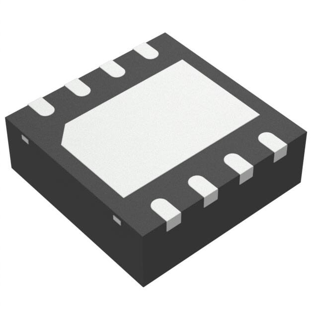
The AST1S31 device is available in a 3 x 3 mm, 8
leads VFDFPN package.
Current foldback short-circuit protection
VFDFPN 3 x 3 - 8L package
Figure 1. Application circuit
/
9,1
9,16:
9287
6:
9,1$
&LQBD
(1
5�
$67�6��
9)%
&LQBVZ
&RXW
3*
*1'
5�
August 2020
This is information on a product in full production.
DocID025467 Rev 7
1/35
www.st.com
�Contents
AST1S31
Contents
1
2
Pin settings . . . . . . . . . . . . . . . . . . . . . . . . . . . . . . . . . . . . . . . . . . . . . . . . 4
1.1
Pin connection . . . . . . . . . . . . . . . . . . . . . . . . . . . . . . . . . . . . . . . . . . . . . . 4
1.2
Pin description . . . . . . . . . . . . . . . . . . . . . . . . . . . . . . . . . . . . . . . . . . . . . . 4
Maximum ratings . . . . . . . . . . . . . . . . . . . . . . . . . . . . . . . . . . . . . . . . . . . . 5
2.1
Thermal data . . . . . . . . . . . . . . . . . . . . . . . . . . . . . . . . . . . . . . . . . . . . . . . 5
2.2
ESD performance . . . . . . . . . . . . . . . . . . . . . . . . . . . . . . . . . . . . . . . . . . . . 5
3
Electrical characteristics . . . . . . . . . . . . . . . . . . . . . . . . . . . . . . . . . . . . . 6
4
Functional description . . . . . . . . . . . . . . . . . . . . . . . . . . . . . . . . . . . . . . . 8
5
4.1
Output voltage adjustment . . . . . . . . . . . . . . . . . . . . . . . . . . . . . . . . . . . . . 9
4.2
Soft-start . . . . . . . . . . . . . . . . . . . . . . . . . . . . . . . . . . . . . . . . . . . . . . . . . . 10
4.3
Error amplifier and control loop stability . . . . . . . . . . . . . . . . . . . . . . . . . . 10
4.4
Overcurrent protection . . . . . . . . . . . . . . . . . . . . . . . . . . . . . . . . . . . . . . . 15
4.5
Enable function . . . . . . . . . . . . . . . . . . . . . . . . . . . . . . . . . . . . . . . . . . . . 17
4.6
Light load operation . . . . . . . . . . . . . . . . . . . . . . . . . . . . . . . . . . . . . . . . . 18
4.7
Hysteretic thermal shutdown . . . . . . . . . . . . . . . . . . . . . . . . . . . . . . . . . . 18
Application information . . . . . . . . . . . . . . . . . . . . . . . . . . . . . . . . . . . . . 19
5.1
Input capacitor selection . . . . . . . . . . . . . . . . . . . . . . . . . . . . . . . . . . . . . . 19
5.2
Inductor selection . . . . . . . . . . . . . . . . . . . . . . . . . . . . . . . . . . . . . . . . . . . 20
5.3
Output capacitor selection . . . . . . . . . . . . . . . . . . . . . . . . . . . . . . . . . . . . 21
5.4
Thermal dissipation . . . . . . . . . . . . . . . . . . . . . . . . . . . . . . . . . . . . . . . . . 22
5.5
Layout consideration . . . . . . . . . . . . . . . . . . . . . . . . . . . . . . . . . . . . . . . . 23
6
Demonstration board . . . . . . . . . . . . . . . . . . . . . . . . . . . . . . . . . . . . . . . 25
7
Typical characteristics . . . . . . . . . . . . . . . . . . . . . . . . . . . . . . . . . . . . . . 27
8
Package information . . . . . . . . . . . . . . . . . . . . . . . . . . . . . . . . . . . . . . . . 31
8.1
2/35
VFDFPN8 (3 x 3 x 1.0 mm) package information . . . . . . . . . . . . . . . . . . . 31
DocID025467 Rev 7
�AST1S31
Contents
9
Ordering information . . . . . . . . . . . . . . . . . . . . . . . . . . . . . . . . . . . . . . . 33
10
Revision history . . . . . . . . . . . . . . . . . . . . . . . . . . . . . . . . . . . . . . . . . . . 34
DocID025467 Rev 7
3/35
35
�Pin settings
AST1S31
1
Pin settings
1.1
Pin connection
Figure 2. Pin connection (top view)
1.2
Pin description
Table 1. Pin description
4/35
No.
Type
Description
1
VINA
2
EN
Enable input. With EN higher than 1.5 V the device in ON and with EN
lower than 0.5 V the device is OFF.
3
FB
Feedback input. Connecting the output voltage directly to this pin the
output voltage is regulated at 0.8 V. To have higher regulated voltages an
external resistor divider is required from VOUT to the FB pin.
4
AGND
Unregulated DC input voltage
Ground
Open drain Power Good (POR) pin. It is released (open drain) when the
output voltage is higher than 0.92 * VOUT with a delay of 170 s. If the
output voltage is below 0.92 * VOUT, the POR pin goes to low impedance
immediately.
If not used, it can be left floating or to GND.
5
PG
6
VINSW
7
SW
8
PGND
Power ground
9
ePAD
Exposed pad connected to ground
Power input voltage
Regulator output switching pin
DocID025467 Rev 7
�AST1S31
2
Maximum ratings
Maximum ratings
Stressing the device above the ratings listed in Table 2: Absolute maximum ratings may
cause permanent damage to the device. These are stress ratings only and operation of the
device at these or any other conditions above those indicated in Table 5: Electrical
characteristics of this specification is not implied. Exposure to absolute maximum rating
conditions may affect device reliability.
Table 2. Absolute maximum ratings
Symbol
2.1
Parameter
Value
Unit
VIN
Input voltage
VEN
Enable voltage
VSW
Output switching voltage
VPG
Power on reset voltage (Power Good)
-0.3 to VIN
VFB
Feedback voltage
-0.3 to 1.5
PTOT
Power dissipation at TA < 60 °C
TOP
Tstg
-0.3 to 5
-0.3 to VIN
-1 to VIN
V
2.25
W
Operating junction temperature range
-40 to 150
°C
Storage temperature range
-55 to 150
°C
Value
Unit
50
°C/W
Thermal data
Table 3. Thermal data
Symbol
RthJA
Parameter
Maximum thermal resistance
junction ambient (1)
VFDFPN
1. Package mounted on demonstration board.
2.2
ESD performance
Table 4. ESD performance
Symbol
ESD
Parameter
ESD protection voltage
DocID025467 Rev 7
Test conditions
Value
Unit
HBM
2
kV
CDM corner pins
750
CDM non-corner pins
500
V
5/35
35
�Electrical characteristics
3
AST1S31
Electrical characteristics
TJ = -40 °C to 125 °C, VIN = 4 V, unless otherwise specified.
Table 5. Electrical characteristics
Values
Symbol
Parameter
Test condition
Unit
Min.
VIN
Typ.
Max.
Operating input voltage range
2.8
VINON
Turn on VCC threshold
2.3
2.45
2.6
VINOFF
Turn off VCC threshold
1.85
2.0
2.15
70
110
RDSON-P
High-side switch onresistance
ISW = 300 mA, TJ = 25 °C
RDSON-N
Low-side switch onresistance
ISW = 300 mA, TJ = 25 °C
ILIM
4
ISW = 300 mA, TJ = 125 °C
140
55
ISW = 300 mA, TJ = 125 °C
90
110
Maximum limiting current
3.6
Switching frequency
1.2
(1)
Io = 10 mA to 4 A
V
m
m
6
A
1.5
1.9
MHz
0.790
0.8
0.810
0.776
0.8
0.824
630
1200
A
1
A
Oscillator
FSW
Dynamic characteristics
VFB
Feedback voltage
V
DC characteristics
IQ
IQST-BY
Quiescent current
Duty cycle = 0, no load VFB = 1.2 V
Total standby quiescent
current
OFF
Enable
VEN
EN threshold voltage
IEN
EN current
Device ON level
1.5
Device OFF level
0.5
V
0.1
A
96
%VFB
400
mV
Power Good
PG threshold
PG
PG output voltage low
92
94
Isink = 6 mA open drain
PG rise delay
170
s
Soft-start duration
400
s
Soft-start
TSS
6/35
DocID025467 Rev 7
�AST1S31
Electrical characteristics
Table 5. Electrical characteristics (continued)
Values
Symbol
Parameter
Test condition
Unit
Min.
Typ.
Max.
Protection
TSHDN
Thermal shutdown
(2)
150
Hysteresis
(2)
20
°C
1. Tj = 25 °C.
2. Guaranteed by design.
DocID025467 Rev 7
7/35
35
�Functional description
4
AST1S31
Functional description
The AST1S31 device is based on a “peak current mode”, constant frequency control. The
output voltage VOUT is sensed by the feedback pin (FB) compared to an internal reference
(0.8 V) providing an error signal that, compared to the output of the current sense amplifier,
controls the ON and OFF time of the power switch.
The main internal blocks are shown in the block diagram in Figure 3. They are:
A fully integrated oscillator that provides the internal clock and the ramp for the slope
compensation avoiding sub-harmonic instability
The soft-start circuitry to limit inrush current during the start-up phase.
The transconductance error amplifier
The pulse width modulator and the relative logic circuitry necessary to drive the internal
power switches.
The drivers for embedded P-channel and N-channel power MOSFET switches.
The high-side current sensing block.
The low-side current sense to implement diode emulation.
A voltage monitor circuitry (UVLO) that checks the input and internal voltages.
A thermal shutdown block, to prevent a thermal runaway.
Figure 3. Block diagram
8/35
DocID025467 Rev 7
�AST1S31
4.1
Functional description
Output voltage adjustment
The error amplifier reference voltage is 0.8 V typical. The output voltage is adjusted
according to the following formula (see Figure 1 on page 1):
Equation 1
R1
V OUT = 0.8 1 + -------
R2
The internal architecture of the device requires a minimum off time, cycle-by-cycle, for the
output voltage regulation. The minimum off time is typically equal to 94 ns.
The control loop compensates for conversion losses with duty cycle control. Since the
power losses are proportional to the delivered output power, the duty cycle increases with
the load current request.
Figure 4 shows the maximum regulated output voltage over the input voltage range at
different loading conditions.
Figure 4. Maximum output voltage over loading conditions
DocID025467 Rev 7
9/35
35
�Functional description
4.2
AST1S31
Soft-start
The soft-start is essential to assure the correct and safe startup of the step-down converter.
It avoids an inrush current surge and makes the output voltage rise monothonically.
The soft-start is managed ramping the reference of the error amplifier from 0 V to 0.8 V. The
internal soft-start capacitor is charged with a resistor to 0.8 V, then the FB pin follows the
reference so that the output voltage is regulated to rise to the set value monothonically.
4.3
Error amplifier and control loop stability
The error amplifier provides the error signal to be compared with the high-side switch
current through the current sense circuitry. The non-inverting input is connected with the
internal 0.8 V reference, whilst the inverting input is the FB pin. The compensation network
is internal and connected between the E/A output and GND.
The error amplifier of the AST1S31 device is a transconductance operational amplifier, with
high bandwidth and high output impedance.
The characteristics of the uncompensated error amplifier are listed in Table 6:
Table 6. Error amplifier characteristics
Description
Value
DC gain
94 dB
gm
228 A/V
RO
212 M
The AST1S31 device embeds the compensation network that assures the stability of the
loop in the whole operating range. On the next pages all the tools needed to check the loop
stability will be explained.
In Figure 5 is shown the simple small signal model for the peak current mode control loop.
10/35
DocID025467 Rev 7
�AST1S31
Functional description
Figure 5. Block diagram of the loop for the small signal analysis
VIN
GCO(s)
Slope
Compensation
High side
Switch
L
Current sense
Logic
And
Driver
VOUT
GDIV (s)
Cout
Low side
Switch
PWM comparator
0.8V
R1
VC
Rc
VFB
Error Amp
R2
Cc
G EA(s)
DocID025467 Rev 7
11/35
35
�Functional description
AST1S31
Three main terms can be identified to obtain the loop transfer function:
1.
From control (output of E/A) to output, GCO(s)
2.
From output (VOUT) to FB pin, GDIV(s)
3.
From FB pin to control (output of E/A), GEA(s).
The transfer function from control to output GCO(s) results:
Equation 2
s
1 + ----
z
R LOAD
1
G CO s = ------------------ --------------------------------------------------------------------------------------------- ---------------------- F H s
R out T SW
Ri
s
------
1 + ---------------------------- m C 1 – D – 0.5 1 +
L
p
where RLOAD represents the load resistance, Ri the equivalent sensing resistor of the
current sense circuitry (0.38 ), p the single pole introduced by the LC filter and z the
zero given by the ESR of the output capacitor.
FH(s) accounts the sampling effect performed by the PWM comparator on the output of the
error amplifier that introduces a double pole at one half of the switching frequency.
Equation 3
1
Z = ------------------------------ESR C OUT
Equation 4
m C 1 – D – 0.5
1
p = -------------------------------------- + --------------------------------------------L C OUT f SW
R LOAD C OUT
where:
Equation 5
Se
m C = 1 + -----Sn
S = V f
pp SW
e
V
IN – V OUT
S = ----------------------------- Ri
n
L
Sn represents the ON time slope of the sensed inductor current, Se the slope of the external
ramp (VPP peak-to-peak amplitude - 0.55 V) that implements the slope compensation to
avoid sub-harmonic oscillations at a duty cycle over 50%.
The sampling effect contribution FH(s) is:
Equation 6
1
F H s = -----------------------------------------2
s
s
1 + ------------------- + ------2
n QP
n
where:
12/35
DocID025467 Rev 7
�AST1S31
Functional description
Equation 7
1
Q P = --------------------------------------------------------- m C 1 – D – 0.5
and
Equation 8
n = f SW
The resistor to adjust the output voltage gives the term from output voltage to the FB pin.
GDIV(s) is:
R2
G DIV s = -------------------R1 + R2
The transfer function from FB to Vc (output of E/A) introduces the singularities (poles and
zeroes) to stabilize the loop. In Figure 6 is shown the small signal model of the error
amplifier with the internal compensation network.
Figure 6. Small signal model for the error amplifier
V FB
Ro
Vd
Gm*Vd
Co
Rc
Cc
Cp
Cc
VREF
RC and CC introduce a pole and a zero in the open loop gain. CP does not significantly affect
system stability and can be neglected.
So GEA(s) results:
Equation 9
G EA0 1 + s R c C c
G EA s = ---------------------------------------------------------------------------------------------------------------------------------------------------------------------------------------2
s R0 C0 + Cp Rc Cc + s R0 Cc + R0 C0 + Cp + Rc Cc + 1
Where GEA = Gm ꞏ Ro
The poles of this transfer function are (if Cc >> C0 + CP):
Equation 10
1
f P LF = ---------------------------------2 R0 Cc
DocID025467 Rev 7
13/35
35
�Functional description
AST1S31
Equation 11
1
f P HF = ---------------------------------------------------2 Rc C0 + Cp
whereas the zero is defined as:
Equation 12
1
f Z = --------------------------------2 Rc Cc
The embedded compensation network is RC = 80 k, CC = 55 pF while CP and CO can be
considered as negligible. The error amplifier output resistance is 212 Mso the relevant
singularities are:
Equation 13
f Z = 36 2 kHz
f P LF = 13 6 Hz
So closing the loop, the loop gain GLOOP(s) is:
Equation 14
G LOOP s = G CO s G DIV s G EA s
Example:
VIN = 3.3 V, VOUT = 1.2 V, Iomax = 3 A, L = 1.0 H, Cout = 47 F (MLCC), R1 = 10 k,
R2 = 20 k.
The module and phase Bode plot are reported in Figure 7.
The bandwidth is 110 kHz and the phase margin is 65 degree.
14/35
DocID025467 Rev 7
�AST1S31
Functional description
Figure 7. Module and phase Bode plot
120
102
84
Module [dB]
66
48
30
12
6
24
42
60
0.1
1
10
100
3
4
1 10
1 10
Frequency [Hz]
0.1
1
10
100
1 10
1 10
Frequency [Hz]
5
1 10
5
1 10
1 10
6
1 10
7
6
1 10
10
17.5
45
Phase
72.5
100
127.5
155
182.5
210
4.4
3
4
1 10
7
Overcurrent protection
The AST1S31 device implements overcurrent protection sensing the current flowing through
the high-side current switch.
If the current exceeds the overcurrent threshold the high-side is turned off, implementing
a cycle-by-cycle current limitation. Since the regulation loop is no more fixing the duty cycle,
the output voltage is unregulated and the FB pin falls accordingly to the new duty cycle.
The mechanism to adjust the switching under current foldback condition exploits the lowside current sense circuitry.
If the FB is lower than 0.2 V, the high-side power MOSFET is turned off after the minimum
conduction time (approximately 100 nsec typ.), then, after a proper deadtime that avoids the
cross conduction, the low-side is turned on until the low-side current is lower than a valley
threshold (1.5 A typ.). Once the low-side is turned off, the high-side is immediately turned
on.
DocID025467 Rev 7
15/35
35
�Functional description
AST1S31
In this way the frequency is adjusted to keep the inductor current ripple between the peak
current value that could be evaluated by the following equation:
Equation 15
V In + V Out – DCR L + R DS on HS I Valley
I Peak = I Valley + ---------------------------------------------------------------------------------------------------------------- T Onmin
L
where DCRL is the series resistance of the inductor and the measured value of valley
current threshold (1.5 A typ.), so properly limiting the output current in case of the
overcurrent or short-circuit.
The overcurrent protection is always effective when VFB < 0.2 V thanks to the natural
frequency reduction.
No frequency foldback is otherwise implemented when VFB > 0.2 V. In this case, when the
current ripple during the on phase is bigger than the one during the off phase, there will be
a peak current level higher than the current limit threshold.
The following equations show the inductor current ripple during the ON and OFF phases in
case of overcurrent condition:
On phase:
Equation 16
V In – V Out – DCR L + R DS on HS I
I Ton = ------------------------------------------------------------------------------------------------- T Onmin
L
Where:
Equation 17
V OUTSet
V Out = V FB ---------------------0.8
It’s also possible to define the output voltage in function of input voltage, on phase time and
switching frequency:
Equation 18
T OnMin
V OUTSet = V IN D MIN = V IN ------------------T SW
So the on phase equation results:
Equation 19
V IN T ONMin
V IN – V FB ----------------------------------- – DCR L + R DS ON HighSide I
0.8 T SW
I TON V FB = ---------------------------------------------------------------------------------------------------------------------------------------------------------- T ONMin
L
Off phase:
Equation 20
– R DS ON LowSide + DCR L I – V OUT
I TOFF = ------------------------------------------------------------------------------------------------------- T SW
L
16/35
DocID025467 Rev 7
�AST1S31
Functional description
It is possible repeat the considerations realized to the on phase equation. So it's possible
write the off phase equation in the following manner:
Equation 21
V IN T ONMin
– R DS ON LowSide + DCR L I – V FB ----------------------------------0.8 T SW
I TOFF V FB = -------------------------------------------------------------------------------------------------------------------------------------------- T SW
L
The peak current escalates over the peak current threshold (called “OCP1”) if:
Equation 22
I TON V FB I TOFF V FB
In case the current escalates up to a further current threshold (called “OCP2”), slightly
higher than the OCP1, the converter stops the switching activity, the reference of the error
amplifier is pulled down and then it restarts with a new soft-start procedure. If the
overcurrent condition is still active, the current foldback with frequency reduction properly
limit the output current.
Figure 8. Overcurrent protection region
4.5
Enable function
The enable feature allows to put the device into the standby mode. With the EN pin lower
than 0.4 V, the device is disabled and the power consumption is reduced to less than 10 A.
With the EN pin higher than 1.2 V, the device is enabled. If the EN pin is left floating, an
internal pull-down ensures that the voltage at the pin reaches the inhibit threshold and the
device is disabled. The pin is also VIN compatible.
DocID025467 Rev 7
17/35
35
�Functional description
4.6
AST1S31
Light load operation
With peak current mode control loop the output of the error amplifier is proportional to the
load current. In order to increase the efficiency in light load conditions, when the output of
the error amplifier falls below a certain threshold, the high-side turn on is prevented.
This mechanism reduces the switching frequency at light load in order to save the switching
losses.
4.7
Hysteretic thermal shutdown
The thermal shutdown block generates a signal that turns off the power stage if the junction
temperature goes above 150 oC. Once the junction temperature goes back to about 130 oC,
the device restarts in normal operation.
18/35
DocID025467 Rev 7
�AST1S31
Application information
5
Application information
5.1
Input capacitor selection
The capacitor connected to the input must be capable of supporting the maximum input
operating voltage and the maximum RMS input current required by the device. The input
capacitor is subject to a pulsed current, the RMS value of which is dissipated over its ESR,
affecting the overall system efficiency.
So the input capacitor must have an RMS current rating higher than the maximum RMS
input current and an ESR value compliant with the expected efficiency.
The maximum RMS input current flowing through the capacitor can be calculated as:
Equation 23
2
2
2D
D
I RMS = I O D – --------------- + ------2
where IO is the maximum DC output current, D is the duty cycle, and is the efficiency.
Considering = 1, this function has a maximum at D = 0.5 and is equal to IO/2.
The peak-to-peak voltage across the input capacitor can be calculated as:
Equation 24
IO
D
D
V PP = ------------------------- 1 – ---- D + ---- 1 – D + ESR I O
C IN F SW
where ESR is the equivalent series resistance of the capacitor.
Given the physical dimension, ceramic capacitors can well meet the requirements of the
input filter sustaining a higher input RMS current than electrolytic / tantalum types. In this
case the equation of CIN as a function of the target peak-to-peak voltage ripple (VPP) can be
written as follows:
Equation 25
IO
D
D
C IN = --------------------------- 1 – ---- D + ---- 1 – D
V PP F SW
neglecting the small ESR of ceramic capacitors.
Considering = 1, this function has its maximum in D = 0.5, therefore, given the maximum
peak-to-peak input voltage (VPP_MAX), the minimum input capacitor (CIN_MIN) value is:
Equation 26
IO
C IN_MIN = -----------------------------------------------2 V PP_MAX F SW
Typically, CIN is dimensioned to keep the maximum peak-to-peak voltage ripple in the order
of 1% of VINMAX.
The placement of the input capacitor is very important to avoid noise injection and voltage
spikes on the input voltage pin. So the CIN must be placed as close as possible to the
DocID025467 Rev 7
19/35
35
�Application information
AST1S31
VIN_SW pin. In Table 7 some multilayer ceramic capacitors suitable for this device are
given.
Table 7. Input MLCC capacitors
Manufacturer
Series
Cap value (µF)
Rated voltage (V)
Murata
GRM21
10
10
C3225
10
25
C3216
10
16
LMK212
22
10
TDK
TAIYO YUDEN
A ceramic bypass capacitor, as close as possible to the VINA pin so that additional parasitic
ESR and ESL are minimized, is suggested in order to prevent instability on the output
voltage due to noise. The value of the bypass capacitor can go from 330 nF to 1 µF.
5.2
Inductor selection
The inductance value fixes the current ripple flowing through the output capacitor. So the
minimum inductance value to have the expected current ripple must be selected. The rule to
fix the current ripple value is to have a ripple at 20% - 40% of the output current.
In continuous current mode (CCM), the inductance value can be calculated by Equation 27:
Equation 27
V IN – V OUT
V OUT
I L = ------------------------------ T ON = -------------- T OFF
L
L
where TON is the conduction time of the high-side switch and TOFF is the conduction time of
the low-side switch (in CCM, FSW = 1/(TON + TOFF)). The maximum current ripple, given the
VOUT, is obtained at maximum TOFF, that is, at the minimum duty cycle (see previous section
to calculate minimum duty). So by fixing IL = 20% to 30% of the maximum output current,
the minimum inductance value can be calculated:
Equation 28
V OUT 1 – D MIN
L MIN = ---------------- ----------------------I MAX F SWMIN
where FSWMIN is the minimum switching frequency, according toTable 5: Electrical
characteristics on page 6. The slope compensation, to prevent the sub-harmonic instability
in the peak current control loop, is internally managed and so fixed. This implies a further
lower limit for the inductor value. To assure sub-harmonic stability:
Equation 29
L V out 2 V pp f sw
where VPP is the peak-to-peak value of the slope compensation ramp. The inductor value
selected based on Equation 28 must satisfy Equation 29.
20/35
DocID025467 Rev 7
�AST1S31
Application information
The peak current through the inductor is given by Equation 30:
Equation 30
I L
I L PK = I O + -------2
So if the inductor value decreases, the peak current (which must be lower than the current
limit of the device) increases. The higher the inductor value, the higher the average output
current that can be delivered, without reaching the current limit.
In Table 8 some inductor part numbers are listed.
Table 8. Inductors
Manufacturer
Coilcraft
Würth
Coiltronics
5.3
Series
Inductor value (µH)
Saturation current (A)
XAL50xx
1.2 to 3.3
6.3 to 9
XAL60xx
2.2 to 5.6
7.4 to 11
MSS1048
1.0 to 3.8
6.5 to 11
WE-HCI 7030
1.5 to 4.7
7 to 14
WE-PD type L
1.5 to 3.5
6.4 to 10
DR73
1.0 to 2.2
5.5 to7.9
DR74
1.5 to 3.3
5.4 to 8.35
Output capacitor selection
The current in the output capacitor has a triangular waveform which generates a voltage
ripple across it. This ripple is due to the capacitive component (charge or discharge of the
output capacitor) and the resistive component (due to the voltage drop across its ESR). So
the output capacitor must be selected in order to have a voltage ripple compliant with the
application requirements.
The amount of the voltage ripple can be calculated starting from the current ripple obtained
by the inductor selection.
Equation 31
I MAX
V OUT = ESR I MAX + ------------------------------------8 C OUT f SW
For a ceramic (MLCC) capacitor, the capacitive component of the ripple dominates the
resistive one. While for an electrolytic capacitor the opposite is true.
As the compensation network is internal, the output capacitor should be selected in order to
have a proper phase margin and then a stable control loop.
The equations of Section 5.2 help to check loop stability given the application conditions,
the value of the inductor and of the output capacitor.
DocID025467 Rev 7
21/35
35
�Application information
AST1S31
In Table 9 some capacitor series are listed.
Table 9. Output capacitors
Series
Cap value (µF)
Rated voltage (V)
ESR (m)
GRM32
22 to 100
6.3 to 25