AN1451
APPLICATION NOTE
L6208 FULLY INTEGRATED TWO PHASE
STEPPER MOTOR DRIVER
by Domenico Arrigo, Vincenzo Marano and Thomas Hopkins
Modern motion control applications need more flexibility that can be addressed only with specialized IC
products. The L6208 is a fully integrated stepper motor driver IC specifically developed to drive a wide range
of two phase (bipolar) stepper motors. This IC is a one-chip cost effective solution that includes several
unique circuit design features. These features, including a decoding logic that can generate three different
stepping sequences, allow the device to be used in many applications including microstepping. The principal
aim of this development project was to produce an easy to use, fully protected power IC. In addition several
key functions such as protection circuit and PWM current control drastically reduce external components
count to meet requirements for many different applications.
1
INTRODUCTION
The L6208 is a highly integrated, mixed-signal power IC that allows the user to easily design a complete motor
control system for two-phase bipolar stepper motors. Figure 1 shows the L6208 block diagram. The IC integrates eight Power DMOS, a centralized logic circuit which implements the phase generation and a constant
tOFF PWM current control technique (Quasi-Synchronous mode) for each of the two phases of the motor plus
other added features for safe operation and flexibility.
Figure 1. L6208 block diagram.
VBOOT
VBOOT
VBOOT
VCP
CHARGE
PUMP
VSA
VBOOT
THERMAL
PROTECTION
OCDA
OVER
CURRENT
DETECTION
OUT1A
OCDB
10V
GATE
LOGIC
EN
CONTROL
SENSEA
PWM
HALF/FULL
CLOCK
RESET
OUT2A
10V
STEPPING
SEQUENCE
GENERATION
ONE SHOT
MONOSTABLE
CW/CCW
MASKING
TIME
+
SENSE
COMPARATOR
VREFA
RCA
BRIDGE A
GND
VOLTAGE
REGULATOR
GND
GND
10V
5V
GND
L6208
VSB
OVER
CURRENT
DETECTION
OUT1B
OUT2B
SENSEB
GATE
LOGIC
VREFB
BRIDGE B
RCB
D01IN1226
October 2003
1/43
�AN1451 APPLICATION NOTE
Table of Contents
1
2
3
4
5
2/43
INTRODUCTION ................................................................................................................................1
DESIGNING AN APPLICATION WITH L6208 ...................................................................................3
2.1 Current Ratings ........................................................................................................................3
2.2 Voltage Ratings and Operating Range ....................................................................................3
2.3 Choosing the Bulk Capacitor....................................................................................................5
2.4 Layout Considerations .............................................................................................................6
2.5 Sensing Resistors ....................................................................................................................8
2.6 Charge pump external components .........................................................................................9
2.7 Sharing the Charge Pump Circuitry .......................................................................................10
2.8 Reference Voltage for PWM Current Control.........................................................................11
2.9 Input Logic pins ......................................................................................................................12
2.10 EN pin ....................................................................................................................................12
2.11 Programmable off-time Monostable ......................................................................................13
2.11.1 Off-time Selection and minimum on-time ........................................................................15
2.11.2 Decay Modes ..................................................................................................................16
2.12 Over Current Protection ........................................................................................................18
2.13 Power Management ..............................................................................................................21
2.13.1 Maximum output current vs. selectable devices..............................................................22
2.13.2 Power Dissipation Formulae for different sequences ......................................................22
2.14 Choosing the Decay Mode....................................................................................................25
2.15 Choosing the Stepping Sequence.........................................................................................26
2.16 Microstepping........................................................................................................................27
APPLICATION EXAMPLE................................................................................................................30
3.1 Decay mode, sensing resistors and reference voltage. .........................................................30
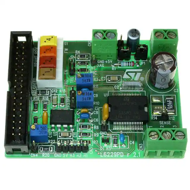
APPENDIX - EVALUATION BOARDS .............................................................................................31
4.1 PractiSPIN..............................................................................................................................31
4.2 EVAL6208N ...........................................................................................................................33
4.2.1 Important Notes ................................................................................................................34
4.2.2 Thermal Impedance .........................................................................................................34
4.3 EVAL6208PD .........................................................................................................................38
4.3.1 Important Notes ................................................................................................................39
4.3.2 Thermal Impedance .........................................................................................................39
REFERENCES.................................................................................................................................43
�AN1451 APPLICATION NOTE
2
DESIGNING AN APPLICATION WITH L6208
2.1 Current Ratings
With MOSFET (DMOS) devices, unlike bipolar transistors, current under short circuit conditions is, at first approximation, limited by the RDS(ON) of the DMOS themselves and could reach very high values. L6208 Out pins
and the two VSA and VSB pins are rated for a maximum of 2.8A r.m.s. and 5.6A peak (typical values), corresponding to a total (for the whole IC) 5.6A rms (11.2A peak). These values are meant to avoid damaging metal
structures, including the metallization on the die and bond wires. In practical applications, though, maximum allowable current is less than these values, due to power dissipation limits (see Power Management section).
The device has a built-in Over Current Detection (OCD) that provides protection against short circuits between
the outputs and between an output and ground (see Over Current Protection section).
2.2 Voltage Ratings and Operating Range
The L6208 requires a single supply voltage (VS), for the motor supply. Internal voltage regulators provide the
5V and 10V required for the internal circuitry. The operating range for VS is 8 to 52V. To prevent working into
undesirable low supply voltage an Under Voltage Lock Out (UVLO) circuit shuts down the device when supply
voltage falls below 6V; to resume normal operating conditions, VS must then exceed 7V. The hysteresis is provided to avoid false intervention of the UVLO function during fast VS ringings. It should be noted, however, that
DMOS's RDS(ON) is a function of the VS supply voltage. Actually, when VS is less than 10V, RDS(ON) is adversely
affected, and this is particularly true for the High Side DMOS that are driven from VBOOT supply. This supply is
obtained through a charge pump from the internal 10V supply, which will tend to reduce its output voltage when
VS goes below 10V. Figure 2 shows the supply voltage of the high side gate drivers (VBOOT - VS) versus the
supply voltage (VS).
Figure 2. High side gate drivers supply voltage versus supply voltage.
8
7 .6
VBOOT - VS
[V]
7 .2
6 .8
6 .4
6
8
8 .5
9
9 .5
10
1 0 .5
VS [V]
Note that VS must be connected to both VSA and VSB since the bootstrap voltage (at VBOOT pin) is the same for
the two H-bridges. The integrated DMOS have a rated Drain-Source breakdown voltage of 60V. However VS
should be kept below 52V, since in normal working conditions the DMOS see a Vds voltage that will exceed VS
supply. In particular, when using the fast decay mode, at the beginning of the off-time (when all the DMOS are
off during dead-time) the SENSE pin sees a negative spike due to a not negligible parasitic inductance of the
PCB path from the pin to GND. This spike is followed by a stable negative voltage due to the drop on RSENSE.
One of the two OUT pins of the bridge sees a similar behavior, but with a slightly larger voltage due to the forward recovery time of the integrated freewheeling diode and the forward voltage drop across it (see Figure 3).
Typical duration of this spike is 30ns. At the same time, the other OUT pin of the same bridge sees a voltage
3/43
�AN1451 APPLICATION NOTE
above VS, due to the PCB inductance and voltage drop across the high-side (integrated) freewheeling diode,
as the current reverses direction and flows into the bulk capacitor. It turns out that, in fast decay, the highest
differential voltage is observed between the two OUT pins of the same bridge, at the beginning of the off-time,
and this must always be kept below 60V [3]. The same high voltage condition exists when a step is made and
the direction of current flow reverses in the bridge.
Figure 3. Currents and voltages during the dead time at the beginning of the off-time.
ESR
VS
PCB Parasitic
Inductance
ESL
Bulk Capacitor
Equivalent Circuit
OUT2
OUT1
RSENSE*I+VF(Diode)
Dangerous
High Differential Voltage
RSENSE*I
VS+VF(Diode)
SENSE
RSENSE
PCB Parasitic
Inductance
Figure 4 shows the voltage waveforms at the two OUT pins referring to a possible practical situation, with a peak
output current of 2.8A, VS = 52V, RSENSE = 0.33Ω, TJ = 25°C (approximately) and a good PCB layout. Below
ground spike amplitude is -2.65V for one output; the other OUT pin is at about 57V. In these conditions, total
differential voltage reaches almost 60V, which is the absolute maximum rating for the DMOS. Keeping differential voltage between two Output pins belonging to the same Full Bridge within rated values is a must that can
be accomplished with proper selection of Bulk capacitor value and equivalent series resistance (ESR), according to current peaks and chopping style and adopting good layout practices to minimize PCB parasitic inductances (see below) [3].
4/43
�AN1451 APPLICATION NOTE
Figure 4. Voltage at the two outputs at the beginning of the off-time.
Out 1
Out 2
2.3 Choosing the Bulk Capacitor
Since the bulk capacitor, placed between VS and GND pins, is charged and discharged during IC operation, its
AC current capability must be greater than the r.m.s. value of the charge/discharge current. This current flows
from the capacitor to the IC during the on-time (tON) and from the IC (in fast decay; from the power supply in
slow decay) to the capacitor during the off-time (tOFF). The r.m.s. value of the current flowing into the bulk capacitor depends on peak output current, output current ripple, switching frequency, duty-cycle and chopping
style. It also depends on power supply characteristics. A power supply with poor high frequency performances
(or long, inductive connections to the IC) will cause the bulk capacitor to be recharged slowly: the higher the
current control switching frequency, the higher the current ripple in the capacitor; r.m.s. current in the capacitor,
however, does not exceed the r.m.s. output current. Bulk capacitor value (C) and the ESR determine the amount
of voltage ripple on the capacitor itself and on the IC. In slow decay, neglecting the dead-time and output current
ripple, and assuming that during the on-time the capacitor is not recharged by the power supply, the voltage at
the end of the on-time is:
t O N
V S – I OUT ⋅ ESR + -------- ,
C
so the supply voltage ripple is:
t O N
I OUT ⋅ ESR + -------- ,
C
where IOUT is the output current. With fast decay, instead, recirculating current recharges the capacitor, causing
the supply voltage to exceed the nominal voltage. This can be very dangerous if the nominal supply voltage is
close to the maximum recommended supply voltage (52V). In fast decay the supply voltage ripple is about:
t ON + t O FF
I OUT ⋅ 2 ⋅ ESR + --------------------------- ,
C
always assuming that the power supply does not recharge the capacitor, and neglecting the output current ripple
and the dead-time. Usually (if C > 100 µF) the capacitance role is much less than the ESR, then supply voltage
ripple can be estimated as:
5/43
�AN1451 APPLICATION NOTE
IOUT · ESR in slow decay
2 · IOUT · ESR in fast decay
For Example, if a maximum ripple of 500mV is allowed and IOUT = 2A, the capacitor ESR should be lower than:
0.5 V
ESR < ------------ = 250mΩ in slow decay, and
2A
1 0.5 V
ESR < --- ⋅ ------------ = 1 25mΩ in fast decay.
2 2A
Actually, current sunk by VSA and VSB pins of the device is subject to higher peaks due to reverse recovery
charge of internal freewheeling diodes. Duration of these peaks is, tough, very short, and can be filtered using
a small value (100÷200 nF), good quality ceramic capacitor, connected as close as possible to the VSA, VSB
and GND pins of the IC. Bulk capacitor will be chosen with maximum operating voltage 25% greater than the
maximum supply voltage, considering also power supply tolerances. For example, with a 48V nominal power
supply, with 5% tolerance, maximum voltage is 50.4V, then operating voltage for the capacitor should be at least
63V.
2.4 Layout Considerations
Working with devices that combine high power switches and control logic in the same IC, careful attention has
to be paid to the PCB layout. In extreme cases, Power DMOS commutation can induce noises that could cause
improper operation in the logic section of the device. Noise can be radiated by high dv/dt nodes or high di/dt
paths, or conducted through GND or Supply connections. Logic connections, especially high-impedance nodes
(actually all logic inputs, see further), must be kept far from switching nodes and paths. With the L6208, in particular, external components for the charge pump circuitry should be connected together through short paths,
since these components are subject to voltage and current switching at relatively high frequency (600kHz). Primary mean in minimizing conducted noise is working on a good GND layout (see Figure 5).
Figure 5. Typical Application and Layout suggestions.
2-Phase
Stepper Motor
D1
D2
C8
C5
R4
OUT1A OUT2A OUT1B OUT2B
VBOOT
CP
VSA
VSB
SENSEA
+
Logic Supply
3.3 ÷ 5 V
SENSEB
CW / CCW
µC
+
R6
-
C6
L6208
RESET
Custom Logic
HALF / FULL
C7
VS = 8 ÷ 52 V
CLOCK
-
EN
R1
VrefA
VrefB
RCA
RCB
GND GND GND GND
C1
C3
C2
Vref = 0 ÷1V
6/43
R5
CONTROL
or
R2
C4
R3
�AN1451 APPLICATION NOTE
High current GND tracks (i.e. the tracks connected to the sensing resistors) must be connected directly to the
negative terminal of the bulk capacitor. A good quality, high-frequency bypass capacitor is also required (typically a 100nF÷200nF ceramic would suffice), since electrolytic capacitors show a poor high frequency performance. Both bulk electrolytic and high frequency bypass capacitors have to be connected with short tracks to
VSA, VSB and GND. On the L6208 GND pins are the Logic GND, since only the quiescent current flows through
them. Logic GND and Power GND should be connected together in a single point, the bulk capacitor, to keep
noise in the Power GND from affecting Logic GND. Specific care should be paid layouting the path from the
SENSE pins through the sensing resistors to the negative terminal of the bulk capacitor (Power Ground). These
tracks must be as short as possible in order to minimize parasitic inductances that can cause dangerous voltage
spikes on SENSE and OUT pins (see the Voltage Ratings and Operating Range section); for the same reason
the capacitors on VSA, VSB and GND should be very close to the GND and supply pins. Refer to the Sensing
Resistors section for information on selecting the sense resistors. Traces that connect to VSA, VSB, SENSEA,
SENSEB, and the four OUT pins must be designed with adequate width, since high currents are flowing through
these traces, and layer changes should be avoided. Should a layer change prove necessary, multiple and large
via holes have to be used. A wide GND copper area can be used to improve power dissipation for the device.
Figure 6 shows two typical situations that must be avoided. An important consideration about the location of the
bulk capacitors is the ability to absorb the inductive energy from the load, without allowing the supply voltage to
exceed the maximum rating. The diode shown in Figure 6 prevents the recirculation current from reaching the
capacitors and will result in a high voltage on the IC pins that can destroy the device. Having a switch or a power
connection that can disconnect the capacitors from the IC, while there is still current in the motor, will also result
in a high voltage transient since there is no capacitance to absorb the recirculation current.
Figure 6. Two situations that must be avoided.
VSA
DON’T put a diode here!
Recirculating current cannot flow into the
bulk capacitor and causes a high voltage
spike that can destroy the IC.
VSB
SENSE A
SENSE B
L6208
+
R5
C6
GND GND GND GND
C7
VS = 8 ÷ 52 V
-
DON’T connect the Logic GND here
Voltage drop due to current in sense
path can disturb logic GND.
7/43
�AN1451 APPLICATION NOTE
2.5 Sensing Resistors
Each motor winding current is flowing through the corresponding sensing resistor, causing a voltage drop that
is used, by the logic, to control the peak value of the load current. Two issues must be taken into account when
choosing the RSENSE value:
– The sensing resistor dissipates energy and provides dangerous negative voltages on the SENSE pin
during the current recirculation. For this reason the resistance of this component should be kept low.
– The voltage drop across RSENSE is compared with the reference voltage (on Vref pin) by the internal
comparator. The lower is the RSENSE value, the higher is the peak current error due to noise on Vref pin
and to the input offset of the current sense comparator: too small values of RSENSE must be avoided.
A good compromise is calculating the sensing resistor value so that the voltage drop, corresponding to the peak
current in the load (Ipeak), is about 0.5 V: RSENSE = 0.5 V / Ipeak.
It should be clear that sensing resistor must absolutely be non-inductive type in order to avoid dangerous negative spikes on SENSE pins. Wire-wounded resistors cannot be used here, while Metallic film resistors are recommended for their high peak current capability and low inductance. For the same reason the connections
between the SENSE pins, C6, C7, VSA, VSB and GND pins (see Figure 5) must be taken as short as possible
(see also the Layout Considerations section).
The average power dissipated by the sensing resistor is:
Fast Decay Recirculation: PR ≈ Irms2 · RSENSE
Slow Decay Recirculation: PR ≈ Irms2 · RSENSE · D,
D is the duty-cycle of the PWM current control, Irms is the r.m.s. value of the load current.
Nevertheless, sensing resistor power rating should be chosen taking into account the peak value of the dissipated power:
2
P R ≈ Ipk ⋅ R S ENSE
,
where Ipk is the peak value of the load current.
Using multiple resistors in parallel will help obtaining the required power rating with standard resistors, and reduce the inductance.
RSENSE tolerance reflects on the peak current error: 1% resistors should be preferred.
The following table shows RSENSE recommended values (to have 0.5V drop on it) and power ratings for typical
examples of current peak values.
8/43
Ipk
RSENSE Value [Ω]
RSENSE Power Rating [W]
0.5
1
0.25
Alternatives
1
0.5
0.5
1.5
0.33
0.75
2 X 1Ω, 0.25W paralleled
3 X 1Ω, 0.25W paralleled
2
0.25
1
4 X 1Ω, 0.25W paralleled
�AN1451 APPLICATION NOTE
2.6 Charge pump external components
An internal oscillator, with its output at CP pin, switches from GND to 10V with a typical frequency of 600kHz
(see Figure 7).
Figure 7. Charge Pump.
V S + 10 V - V D 1
V S + 10 V - V D 1 - V D 2
f = 600 kH z
V S - V D1
C8
D1
D2
C5
R4
V B O OT
T o H igh -Side
G ate D r ivers
CP
V SA
V SB
10 V
R D S(O N ) = 70Ω
C h arge Pu mp
O scillator
10 V
5V
10 V
R DS (ON ) = 70Ω
f = 600 kHz
L 6208
When the oscillator output is at ground, C5 is charged by VS through D2. When it rises to 10V, D2 is reverse
biased and the charge flows from C5 to C8 through D1, so the VBOOT pin, after a few cycles, reaches the maximum voltage of VS + 10V - VD1 - VD2, which supplies the high-side gate drivers.
With a differential voltage between VS and VBOOT of about 9V and both the bridges switching at 50kHz, the typical current drawn by the VBOOT pin is 1.85 mA.
Resistor R4 is added to reduce the maximum current in the external components and to reduce the slew rate of
the rising and falling edges of the voltage at the CP pin, in order to minimize interferences with the rest of the
circuit. For the same reason care must be taken in realizing the PCB layout of R4, C5, D1, D2 connections (see
also the Layout Considerations section). Recommended values for the charge pump circuitry are:
D1, D2 : 1N4148
R4
: 100 Ω
C5
: 10nF 100V ceramic
C8
: 220nF 25V ceramic
(1/8 W)
Due to the high charge pump frequency, fast diodes are required. Connecting the cold side of the bulk capacitor
(C8) to VS instead of GND the average current in the external diodes during operation is less than 10 mA (with
R4 = 100 Ω); at startup (when VS is provided to the IC) is less than 200 mA while the reverse voltage is about
10 V in all conditions. 1N4148 diodes withstand about 200 mA DC (1 A peak), and the maximum reverse voltage
is 75 V, so they should fit for the majority of applications.
9/43
�AN1451 APPLICATION NOTE
2.7 Sharing the Charge Pump Circuitry
If more than one device is used in the application, it's possible to use the charge pump from one L6208 to supply
the VBOOT pins of several ICs. The unused CP pins on the slaved devices are left unconnected, as shown in
Figure 8. A 100nF capacitor (C8) should be connected to the VBOOT pin of each device.
Supply voltage pins (VS) of the devices sharing the charge pump must be connected together.
The higher the number of devices sharing the same charge pump, the lower will be the differential voltage available for gate drive (VBOOT - VS), causing a higher RDS(ON) for the high side DMOS, so higher dissipating power.
In this case it's recommended to omit the resistor on the CP pin, obtaining a higher current capability of the
charge pump circuitry.
Better performance can also be obtained using a 33nF capacitor for C5 and using schottky diodes (for example
BAT47 are recommended).
Sharing the same charge pump circuitry for more than 3÷4 devices is not recommended, since it will reduce the
VBOOT voltage increasing the high-side MOS on-resistance and thus power dissipation.
Figure 8. Sharing the charge pump circuitry.
To other Devices
D1 = BAT47
D2 = BAT47
C8 = 100nF
C18 = 100 nF
C5 = 33nF
VBOOT
CP
VSA
VSB
To High-Side
Gate Drivers
CP
VSA
VSB
To High-Side
Gate Drivers
L6208
10/43
VBOOT
L6208
�AN1451 APPLICATION NOTE
2.8 Reference Voltage for PWM Current Control
The device has two analog inputs, VrefA and VrefB, connected to the internal sense comparators, to control the
peak value of the motor current through the integrated PWM circuitry. In typical applications these pins are connected together, in order to obtain the same current in the two motor windings (one exception is the microstepping operation; see the related section). A fixed reference voltage can be easily obtained through a resistive
divider from an available 5 V voltage rail (maybe the one supplying the µC or the rest of the application) and
GND.
A very simple way to obtain a variable voltage without using a DAC is to low-pass filter a PWM output of a µC
(see Figure 9).
Assuming that the PWM output swings from 0 to 5V, the resulting voltage will be:
5V ⋅ D µC ⋅ R DIV
V re f = ---------------------------------------R LP + R DIV
where DµC is the duty-cycle of the PWM output of the µC.
Assuming that the µC output impedance is lower than 1kΩ, with RLP = 56kΩ, RDIV = 15kΩ, CLP = 10nF and a
µC PWM switching from 0 to 5V at 100kHz, the low pass filter time constant is about 0.12 ms and the remaining
ripple on the Vref voltage will be about 20 mV. Using higher values for RLP, RDIV and CLP will reduce the ripple,
but the reference voltage will take more time to vary after changing the duty-cycle of the µC PWM, and too high
values of RLP will also increase the impedance of the Vref net at low frequencies, causing a poor noise immunity.
As sensing resistor values are typically kept small, a small noise on Vref input pins might cause a considerable
error in the output current. It's then recommended to decouple these pins with ceramic capacitors of some tens
of nF, placed very close to Vref and GND pins. Note that Vref pins cannot be left unconnected, while, if connected
to GND, zero current is not guaranteed due to voltage offset in the sense comparator. The best way to cut down
(IC) power consumption and clear the load current is pulling down the EN pin. In slow decay, with very small
reference voltage, PWM integrated circuitry can loose control of the current due to the minimum allowed duration of tON (see the Programmable off-time Monostable section).
Figure 9. Obtaining a variable voltage through a PWM output of a µC.
PWM Output
of a µC
RLP
V ref
RDIV
CLP
GND
11/43
�AN1451 APPLICATION NOTE
2.9 Input Logic pins
CW/CCW, CONTROL, RESET, HALF/FULL, CLOCK are CMOS/TTL compatible logic input pins. The input comparator has been realized with hysteresis to ensure the required noise immunity. Typical values for turn-on and turn-off
thresholds are Vth,ON = 1.8V and Vth,OFF = 1.3V. Pins are ESD protected (see Figure 10) (2kV human-body electrostatic discharge), and can be directly connected to the logic outputs of a µC; a series resistor is generally not recommended, as it could help inducted noise to disturb the inputs. All logic pins enforce a specific behavior and cannot be
left unconnected.
Figure 10. Logic input pins.
CONTROL,
HALF/FULL, CLOCK,
RESET, CW/CCW
5V
ESD
Protection
2.10 EN pin
The EN pin is, actually, bi-directional: as an input, with a comparator similar to the other logic input pins (TTL/CMOS
with hysteresis), it controls the state of the PowerDMOS. When this pin is at a low logic level, all the PowerDMOS are
turned off. The EN pin is also connected to the open drain output of the protection circuit that will pull the pin to GND
if over current or over temperature conditions exist. For this reason, EN pin must be driven through a series resistor
of 2.2kΩ minimum (for 5V logic), to allow the voltage at the pin to be pulled below the turn-off threshold.
A capacitor (C1 in Figure 5) connected between the EN pin and GND is also recommended, to reduce the r.m.s. value
of the output current when overcurrent conditions persist (see Over Current Protection section). EN pin must not be
left unconnected.
Figure 11. EN input pin.
5V
EN
ESD
Protection
12/43
�AN1451 APPLICATION NOTE
2.11 Programmable off-time Monostable
The L6208 includes a constant off time PWM current controller for each of the two bridges. The current control
circuit senses the bridge current by sensing the voltage drop across an external sense resistor connected between the source of the two lower power MOS transistors and ground, as shown in Figure 12. As the current in
the motor builds up the voltage across the sense resistor increases proportionally. When the voltage drop
across the sense resistor becomes greater than the voltage at the reference input (VREFA or VREFB) the sense
comparator triggers the monostable switching the bridge off. The power MOS remain off for the time set by the
monostable and the motor current recirculates as defined by the selected decay mode, described in the next
section. When the monostable times out the bridge will again turn on. Since the internal dead time, used to prevent cross conduction in the bridge, delays the turn on of the power MOS, the effective off time is the sum of the
monostable time plus the dead time.
Figure 12. PWM Current Controller Simplified Schematic
VSA (or B)
TO GATE LOGIC
BLANKING TIME
MONOSTABLE
1µs
FROM THE
LOW-SIDE
GATE DRIVERS
5mA
2H
S
Q
(0)
(1)
MONOSTABLE
SET
1H
IOUT
BLANKER
R
OUT2A(or B)
DRIVERS
+
DEAD TIME
-
DRIVERS
+
DEAD TIME
+
5V
2 PHASE
STEPPER MOTOR
OUT1A(or B)
2.5V
SENSE
COMPARATOR
2L
1L
+
COMPARATOR
OUTPUT
RCA(or B)
COFF
ROFF
-
VREFA(or B)
SENSEA(or B)
RSENSE
D01IN1332
Figure 13 shows the typical operating waveforms of the output current, the voltage drop across the sensing resistor, the RC pin voltage and the status of the bridge. More details regarding the Synchronous Rectification and
the output stage configuration are included in the next section.
Immediately after the Power MOS turns on, a high peak current flows through the sensing resistor due to the
reverse recovery of the freewheeling diodes. The L6208 provides a 1µs Blanking Time tBLANK that inhibits the
comparator output so that this current spike cannot prematurely re-trigger the monostable.
13/43
�AN1451 APPLICATION NOTE
Figure 13. Output Current Regulation Waveforms
IOUT
VREF
RSENSE
tOFF
tON
tOFF
1µs tBLANK
1µs tBLANK
VSENSE
VREF
Slow Decay
0
Slow Decay
ay
ay
c
Fast De
c
Fast De
tRCRISE
VRC
tRCRISE
5V
2.5V
tRCFALL
tRCFALL
1µs tDT
1µs tDT
ON
OFF
SYNCHRONOUS OR QUASI
SYNCHRONOUS RECTIFICATION
D01IN1334
B
C
D
A
B
C
D
Figure 14 shows the magnitude of the Off Time tOFF versus COFF and ROFF values. It can be approximately calculated from the equations:
tRCFALL = 0.6 · ROFF · COFF
tOFF = tRCFALL + tDT = 0.6 · ROFF · COFF + tDT
where ROFF and COFF are the external component values and tDT is the internally generated Dead Time with:
20KΩ ≤ ROFF ≤ 100KΩ
0.47nF ≤ COFF ≤ 100nF
tDT = 1µs (typical value)
Therefore:
tOFF(MIN) = 6.6µs
tOFF(MAX) = 6ms
These values allow a sufficient range of tOFF to implement the drive circuit for most motors.
The capacitor value chosen for COFF also affects the Rise Time tRCRISE of the voltage at the pin RCA (or RCB).
The Rise Time tRCRISE will only be an issue if the capacitor is not completely charged before the next time the
monostable is triggered. Therefore, the on time tON, which depends by motors and supply parameters, has to
be bigger than tRCRISE for allowing a good current regulation by the PWM stage. Furthermore, the on time tON
14/43
�AN1451 APPLICATION NOTE
can not be smaller than the minimum on time tON(MIN).
t O N > t O N ( MIN ) = 1.5µ s (typ. value)
t O N > t RCRISE – t DT
tRCRISE = 600 · COFF
2.11.1 Off-time Selection and minimum on-time
Figure 14 also shows the lower limit for the on time tON for having a good PWM current regulation capacity. It
has to be said that tON is always bigger than tON(MIN) because the device imposes this condition, but it can be
smaller than tRCRISE - tDT. In this last case the device continues to work but the off time tOFF is not more constant.
So, small COFF value gives more flexibility for the applications (allows smaller on time and, therefore, higher
switching frequency), but, the smaller is the value for COFF, the more influential will be the noises on the circuit
performance.
Figure 14. Off-time selection and minimum on-time.
4
1 . 10
R = 100 kΩ
R = 47 kΩ
to f f [ u s]
1 . 10
R = 20 kΩ
3
100
10
1
0.1
1
10
100
10
100
Coff [nF]
to n ( m in ) [ u s]
100
10
1
0.1
1
Coff [nF]
15/43
�AN1451 APPLICATION NOTE
2.11.2 Decay Modes
The CONTROL input is used to select the behavior of the bridge during the off time. When the CONTROL pin
is low, the Fast Decay mode is selected and both transistors in the bridge are switched off during the off time.
When the CONTROL pin is high, the Slow Decay mode is selected and only the low side transistor of the bridge
is switched off during the off time.
Figure 15 shows the operation of the bridge in the Fast Decay mode. At the start of the off time, both of the power
MOS are switched off and the current recirculates through the two opposite free wheeling diodes. The current
decays with a high di/dt since the voltage across the coil is essentially the power supply voltage. After the dead
time, the lower power MOS in parallel with the conducting diode is turned on in synchronous rectification mode.
In applications where the motor current is low it is possible that the current can decay completely to zero during
the off time. At this point if both of the power MOS were operating in the synchronous rectification mode it would
then be possible for the current to build in the opposite direction. To prevent this only the lower power MOS is
operated in synchronous rectification mode. This operation is called Quasi-Synchronous Rectification Mode.
When the monostable times out, the power MOS are turned on again after some delay set by the dead time to
prevent cross conduction.
Figure 16 shows the operation of the bridge in the Slow Decay mode. At the start of the off time, the lower power
MOS is switched off and the current recirculates around the upper half of the bridge. Since the voltage across
the coil is low, the current decays slowly. After the dead time the upper power MOS is operated in the synchronous rectification mode. When the monostable times out, the lower power MOS is turned on again after some
delay set by the dead time to prevent cross conduction.
Figure 15. Fast Decay Mode Output Stage Configurations
A) ON TIME
B) 1µs DEAD TIME
D01IN1335
C) QUASI-SYNCHRONOUS
RECTIFICATION
D) 1µs SLOW DECAY
Figure 16. Slow Decay Mode Output Stage Configurations
A) ON TIME
B) 1µs DEAD TIME
D01IN1336
16/43
C) SYNCHRONOUS
RECTIFICATION
D) 1µs DEAD TIME
�AN1451 APPLICATION NOTE
In some conditions (short off-time, very low regulated current, high motor winding L / R) the system may need
an on-time shorter than 1.5µs. In these cases the PWM current controller can loose the regulation.
Figure 17 shows the operation of the circuit in this condition. When the current first reaches the threshold, the
bridge is turned off for a fixed time and the current decays. During the following on-time current increases above
the threshold, but the bridge cannot be turned off until the minimum 1.5µs on-time expires. Since current increases more in each on-time than it decays during the off-time, it keeps growing during each cycle, with steady
state asymptotic value set by duty-cycle and load DC resistance: the resulting peak current will be
Ipk = VS · D / RLOAD,
where D = tON / (tON + tOFF) is the duty-cycle and RLOAD is the load DC resistance.
Figure 17. Minimum on-time can cause the PWM controller to loose the regulation.
minimum tON
is about 1.5 µs
Vref / RSENSE
needed t ON is less
than 1.5 µs
17/43
�AN1451 APPLICATION NOTE
2.12 Over Current Protection
To implement an Over Current (i.e. short circuit) Protection, a dedicated Over Current Detection (OCD) circuitry
(see Figure 18 for a simplified schematic) senses the current in each high side. Power DMOS are actually made
up with thousands of individual identical cells, each carrying a fraction of the total current flowing. The current
sensing element, connected in parallel to the Power DMOS, is made only with few such cells, having a 1:N ratio
compared to the power DMOS. The total drain current is split between the output and the sense element according to the cell ratio. Sensed current is, then, a small fraction of the output current and will not contribute
significantly to power dissipation.
Figure 18. Over Current Detection simplified circuitry.
OUT1A
VSA
OUT2A
POWER SENSE
1 cell
HIGH SIDE DMOSs OF
THE BRIDGE A
I1A
POWER DMOS
n cells
TO GATE
LOGIC
µC or LOGIC
POWER DMOS
n cells
POWER SENSE
1 cell
+
OCD
COMPARATOR
+5V
I2A
I1A / n
I2A / n
(I1A+I2A) / n
REN.
CEN.
EN
IREF
INTERNAL
OPEN-DRAIN
RDS(ON)
60Ω TYP.
OVER TEMPERATURE
OCD
COMPARATOR
FROM THE
BRIDGE B
D01IN1337
This sensed current is compared to an internally generated reference to detect an over current condition. An
internal open drain mosfet turns on when the sum of the currents in the bridges 1A and 2A or 1B and 2B reaches
the threshold (5.6A typical value); the open drain is internally connected to the EN pin. To ensure an over current
protection, connect this pin to an external RC network (see Figure 18).
Figure 19 shows the device operating in overcurrent condition (short to ground). When an over current is detected the internal open drain mosfet pulls the EN pin to GND switching off all 8 power DMOS of the device and
allowing the current to decay. Under a persistent over current condition, like a short to ground or a short between
two output pins, the external RC network on the EN pin (see Figure 18) reduces the r.m.s. value of the output
current by imposing a fixed disable-time after each over current occurrence. The values of REN and CEN are
selected to ensure proper operation of the device under a short circuit condition. When the current flowing
through the high side DMOS reaches the OCD threshold (5.6 A typ.), after an internal propagation delay
(tOCD(ON)) the open drain starts discharging CEN. When the EN pin voltage falls below the turn-off threshold
(VTH(OFF)) all the Power DMOS turn off after the internal propagation delay (tD(OFF)EN). The current begins to
decay as it circulates through the freewheeling diodes. Since the DMOS are off, there is no current flowing
through them and no current to sense so the OCD circuit, after a short delay (tOCD(OFF)), switches the internal
open drain device off, and REN can charge CEN. When the voltage at EN pin reaches the turn-on threshold
(VTH(ON)), after the tD(ON)EN delay, the DMOS turn on and the current restarts. Even if the maximum output current can be very high, the external RC network provides a disable time (tDISABLE) to ensure a safe r.m.s. value
(see Figure 19).
18/43
�AN1451 APPLICATION NOTE
Figure 19. Over Current Operation.
tDELAY
tDISABLE
tOCD(ON)
Output Current
Output Current
IS OVER
tEN(FALL)
tD(OFF)EN
VTH(OFF)
tOCD(OFF)
tD(ON)EN
tDISABLE
EN
VTH(ON)
VEN(LOW)
EN
tEN(RISE)
The maximum value reached by the current depends on its slew-rate, so on the short circuit nature and supply
voltage, and on the total intervention delay (tDELAY). It can be noticed that after the first current peak, the maximum value reached by the output current becomes lower, because the capacitor on EN pin is discharged starting from a lower voltage, resulting in a shorter tDELAY.
The following approximate relations estimate the disable time and the first OCD intervention delay after the short
circuit (worst case).
The time the device remains disabled is:
tDISABLE = tOCD(OFF) + tEN(RISE) + tD(ON)EN
where
V DD – V E N ( L O W )
t EN ( RISE ) = R EN ⋅ C EN ⋅ ln -------------------------------------------V DD – V TH ( O N )
VEN(LOW) is the minimum voltage reached by the EN pin, and can be estimated with the relation:
V EN ( LO W ) = V T H ( O FF ) ⋅ e
tD ( OFF )EN + t O CD ( OFF )
----------------------------------------------------------R OP DR ⋅ C EN
The total intervention time is
tDELAY = tOCD(ON) + tEN(FALL) + tD(OFF)EN
where
V DD
t EN ( FAL L ) = R OPDR ⋅ C EN ⋅ ln ------------------------V TH ( O FF )
tOCD(OFF), tOCD(ON), tD(ON)EN, tD(OFF)EN, and ROPDR are device intrinsic parameters, VDD is the pull-up voltage
19/43
�AN1451 APPLICATION NOTE
applied to REN.
The external RC network, CEN in particular, must be chosen obtaining a reasonable fast OCD intervention (short
tDELAY) and a safe disable time (long tDISABLE). Figure 20 shows both tDISABLE and tDELAY as a function of CEN:
at least 100µs for tDISABLE are recommended, keeping the delay time below 1÷2µs at the same time.
The internal open drain can also be turned on if the device experiences an over temperature (OVT) condition.
The OVT will cause the device to shut down when the die temperature exceeds the OVT threshold
(TJ>165 °C typ.). Since the OVT is also connected directly to the gate drive circuit (see Figure 1), all the Power
DMOS will shut down, even if EN pin voltage is still over Vth(OFF). When the junction temperature falls below the
OVT turn-off threshold (150 °C typ.), the open drain turns off, CEN is recharged up to VTH(ON) and then the PowerDMOS are turned on back.
Figure 20. Typical disable and delay time as a function of C EN, for several values of REN.
R
3
1 .1 0
EN
= 220 kΩ
R
EN
= 100 kΩ
R
R
tDISABLE [µs]
R
100
10
1
1
10
C
EN
100
[n F ]
tDELAY [µs]
10
1
0 .1
1
10
C
20/43
EN
[n F ]
100
EN
= 47 kΩ
= 33 kΩ
EN
= 10 kΩ
EN
�AN1451 APPLICATION NOTE
2.13 Power Management
Even when operating at current levels well below the maximum ratings of the device, the operating junction temperature must be kept below 125 °C.
Figure 21 shows the IC dissipated power versus the r.m.s. load current, in 4 different driving sequences, assuming the supply voltage is 24V.
Figure 21. IC Dissipated Power versus Output Current.
HALF STEP
IA
10
8
I OUT
IB
6
I OUT
PD [W]
4
Test Conditions:
Supply Voltage = 24V
No PWM
f SW = 30 kHz (slow decay)
2
0
0
0.5
1
1.5
2
2.5
3
I OUT [A]
NORM AL DRIVE
IA
10
8
I OUT
IB
6
I OUT
PD [W ]
4
Test Conditions:
Supply Volt age =24 V
2
0
0
0.5
1
1.5
2
2.5
No PWM
f SW = 30 kHz (slow decay)
3
I OUT [A ]
WAVE DRIVE
IA
10
8
I OUT
IB
6
PD [W]
I OUT
4
Test Conditions:
Supply Voltage = 24V
2
0
0
0.5
1
1.5
2
2.5
No PW M
fSW = 3 0 kHz (slow decay)
3
I OUT [A]
MICROSTEPPING
IA
10
I OUT
8
I OUT
6
IB
PD [W]
4
2
0
0
0.5
1
1.5
I OUT [A]
2
2.5
3
Test Conditions:
Supply Voltage = 24V
f SW = 30 kHz (slow decay)
f SW = 50 kHz (slow decay)
21/43
�AN1451 APPLICATION NOTE
2.13.1 Maximum output current vs. selectable devices
Figure 22 reports a performance comparison between L6228 (std. power) and L6208 (high power) for different
packages, with the following assumptions:
- Normal Drive Mode (two-phase on)
- Supply voltage: 24 V; Switching frequency: 30 kHz.
- Tamb = 25 °C, TJ = 125 °C.
- Maximum RDS(ON) (taking into account process spread) has been considered, @ 125 °C.
- Maximum quiescent current IQ (taking into account process spread) has been considered.
- PCB is a FR4 with a dissipating copper surface on the top side of 6 cm2 (with a thickness of 35 µm) for
SO and PowerDIP packages (D, N suffixes).
- PCB is a FR4 with a dissipating copper surface on the top side of 6 cm2 (with a thickness of 35 µm), 16
via holes and a ground layer for the PowerSO package (PD suffix).
- For each device (on the x axis) y axis reports the maximum output current.
Figure 22. Maximum output current vs. selectable devices.
1 .7 0
1 .5 0
1 .3 0
1 .1 0
Load Current
[A]
0 .9 0
0 .7 0
8 PD
L620
8N
L620
8D
L620
8 PD
L622
8N
L622
L622
8D
0 .5 0
2.13.2 Power Dissipation Formulae for different sequences
Figure 23 to Figure 26 are screenshots of a spreadsheet that helps calculating power dissipation in specified
conditions (application and motor data), and estimates the resulting junction temperature for a given package
and copper area available on the PCB [6]. The model considers power dissipation during the on-time and the
off-time, taking into account the selected decay, rise and fall time (when a phase change occurs) considering
the operating sequence, the switching losses and the quiescent current power dissipation.
22/43
�AN1451 APPLICATION NOTE
Figure 23. Definition of parameters for the three different sequences. The current in only one phase
is shown.
NORMAL
I
WAVE
I
T
T/2
∆I
Ipk
∆I
Iload
Ipk
Iload
t
Tr
Tload
t
Tf
Tr
Tload
Tf
HALF STEP
I
T
∆I
Iload
Ipk
t
Tr
Tload
Tf
Figure 24. Input Data.
Input Data
Device Input Values
Maximum Drain-Source ON Resistance
Ron
=
5.60E-01
[Ohm]
Maximum diode voltage
Vd
=
1.20E+00
[V]
Iq
=
5.50E-03
[mA]
Quiescent Current
Average Value between High-Side and Low-Side
Motor Input Values
Maximum BEMF Voltage
Vb
=
1.50E+01
[V]
Motor Inductance
Lm
=
7.90E-03
[H]
Rm
=
6.60E+00
[Ohm]
Motor Resistance
Application Input Values
Supply Voltage
Vs
=
2.40E+01
[V]
Peak Current
Ipk
=
1.00E+00
[A]
Off-Time
tOFF
=
1.50E-05
[s]
Step Frequency
fCK
=
1.00E+03
[Hz]
Sensing Resistance
Rs
=
5.00E-01
[Ohm]
Decay Type
SLOW
-
"SLOW" = Synchronous Slow Decay
"FAST" = Quasi-Synchronous Fast decay
Stepping sequence
WAVE
-
"NORMAL", "HALF" or "WAVE"
23/43
�AN1451 APPLICATION NOTE
Figure 25. Power Dissipation formulae and results.
Result
PowerDMOS
Commutation
Time
Rise Time
Tcom = 9.60E-08
[s]
Vs / (250V/µs)
Trise =
[s]
( – Ipk ⋅ Rm – 2 ⋅ Ipk ⋅ Ron – Ipk ⋅ Rs + Vs )
Lm
– ln --------------------------------------------------------------------------------------------------------------- ⋅ ---------------------------------------------Vs
Rm + Rs + 2Ron
4.03E-04
Vs
Lm
– ln ------------------------------------------------------------------------------------------------------------- ⋅ ------------------------------------------------------( Ipk ⋅ Rm + 2 ⋅ Ipk ⋅ Ron + Ipk ⋅ Rs + Vs ) ( Rm + 2 ⋅ Ron + Rs )
Fall Time
Tfall =
3.16E-04
NORMAL Mode
[s]
( Vs – 2 ⋅ Vd )
Lm
– ln ------------------------------------------------------------------------------------------- ⋅ ---------------------------( Ipk ⋅ Rm + Ipk ⋅ Rs + Vs – 2 ⋅ Vd ) ( Rm + Rs )
HALF or WAVE
Mode
Duty Cycle
D=
6.25E-01
-
Vb / Vs
(Vs + Vb) / 2Vs
Switching
Frequency
fSW =
2.50E+04
[Hz]
(1-D) / tOFF
Current Ripple
∆I =
2.85E-02
[A]
(Vs - Vb)*D / (Lm* fSW)
Period
T=
2.00E-03
[s]
2 / fCK
4 / fCK
2 / fCK
NORMAL Mode
HALF Mode
WAVE Mode
Tload = 5.97E-04
[s]
T-Trise-Tfall
(3/4)T-rise
(T/2)-Trise
NORMAL Mode
HALF Mode
WAVE Mode
∆I
Ipk – ----2
Load Time
Average Current during
Load Time
I=
9.86E-01
[A]
r.m.s. Current
during Load
Time
Irms =
9.86E-01
[A]
Rise Time
Dissipating
Energy
Erise =
1.50E-04
[J]
Sync. Slow Decay
Quasi-Sync Fast Decay
2
∆I
Ipk ⋅ ( Ipk – ∆I ) + ------3
2 Trise
2Ron ⋅ Ipk ⋅ --------------3
2 Tfall
2Ron ⋅ Ipk ⋅ ------------3
Fall Time
Dissipating
Energy
Efall = 3.62E-04
( – V s + 2 ⋅ V d)
2 ⋅ V d Tfall ⋅ -------------------------------------- +
( Rm + Rs )
[J]
– T fal l
1 – exp ---------------- ⋅ ( Rm + Rs )
Lm
Lm ⋅ ( Ipk ⋅ Rm + Ipk ⋅ Rs + Vs – 2 ⋅ Vd ) ⋅ -------------------------------------------------------------------------------2
( Rm + Rs )
Load Time
Diss. Energy
Eload = 6.50E-05
[J]
2Ron · Irms2 · Tload
2Ron · Irms · D ·Tload + (Ron · Irms2 + Vd · I) · (1 - D) · Tload
Commutatiion
Time
Dissipating Pw
Ecom = 6.78E-05
[J]
2Vs · I · Tcom · Tload · fSW
Quiescent
Dissipating Pw
Pq = 1.32E-01
[W]
Vs · Iq
1.36E+00
[W]
2
--- ·(Erise + Efall + Eload + Ecom) + Pq
T
Total Dissipating Power
24/43
P=
MORMAL Mode
2
HALF or WAVE
Mode
Sync. Slow Decay
Quasi-Sync Fast Decay
�AN1451 APPLICATION NOTE
Figure 26. Thermal Data inputs and results.
Input Data
Package
Copper Area
Copper Area is on
Ground Layer
Am bient Tem perature
SO24
4.0
1÷10 sq. cm
Sam e side of the device
N/A
50
-25 ÷ 100 ºC
Results
Therm al Resistance
Junction to Am bient
53.36
ºC / W
Therm al Resistance
Junction to Pins / Slug
14.00
ºC / W
Estim ated Junction
Tem perature
122.66
ºC
Estim ated
Pins / Slug Tem perature
103.60
2.14 Choosing the Decay Mode
L6208 can operate in either fast or slow decay mode, each having a specific recirculation path for the current
during off-time. In slow decay mode only the lower DMOS is turned off and the current recirculates around the
upper half of the bridge so that voltage across the coil is essentially 0. In Fast decay mode both DMOS are
turned off and the current recirculates back to the power supply rail so that voltage across the coil is essentially
power supply voltage itself.
Slow decay operation provides several advantages: for a given peak current and off-time, current ripple is minimized, and the same is true for acoustic noise and losses in the motor iron (achieving the same current ripple
with fast decay mode would require a shorter off-time resulting in a higher switching frequency and higher power
dissipation in the IC). As current recirculates in the upper half of the bridge and both the high side DMOS in the
same bridge are on, synchronous rectification is realized, minimizing power dissipation in the power switches.
Also, as no output pin goes below GND (see Supply Voltage Ratings and Operating Range section), no power
is dissipated on the sense resistor during the off-time (see Sensing Resistors section).
On the other hand, slow decay can be undesirable in some situations, for example when current has to be regulated at very low values or motor winding L / R ratio is high. In these cases an on-time shorter than the minimum
tON (about 1.5µs) may be requested to regulate the current, and this can cause the PWM controller to loose the
regulation (refer to the Programmable off-time Monostable section).
Another situation where fast decay is to be preferred to slow decay is with regulated current expected to vary
over time with a given profile (enforced providing a variable voltage on the Vref pins, see also Microstepping
section). Here fast decay helps following fast decreasing edges in the desired profile.
25/43
�AN1451 APPLICATION NOTE
2.15 Choosing the Stepping Sequence
The device can provide three different sequences to run a stepper motor: full step two phase on (Normal drive),
full step one phase on (Wave drive) and Half step.
If Half Step driving is used, the motor advances by half a step after each clock pulse, obtaining a higher position
resolution and reducing instability due to low-torque regions in certain motors' speed-torque diagrams, when
used in full step mode (see Figure 27).
Figure 27. Torque instability in full step mode.
Torque
Speed
Using this driving method the torque is affected by ripple, because in odd-numbered states, when both coils are
driven, the total current in the motor windings is double than in even-numbered states.
A way to avoid the high torque ripple in half step mode is to supply to the motor a higher current (by a factor of
2 ) during the even numbered states, in which only one winding is energized, simply by applying a 2 higher
reference voltage at the VrefA, VrefB pins during these states (see Figure 28) [2].
Figure 28. Balanced Half Step for low torque ripple.
IA
Balanced Half Step
3
4
2
1
5
IB
6
8
7
√2
Vref*√
V ref A=V ref B
Vref
Startup or
Reset
Clock 1
26/43
2
3
4
5
6
7
8
�AN1451 APPLICATION NOTE
A simple circuit to generate two different reference voltages is shown in Figure 29. R1 and R2 should be chosen
to have
R2
V re f, HIG H = Vre f ⋅ 2 = 5V ⋅ -------------------R1 + R2
and R3 should be
R1 ⋅ R 2
R 3 = --------------------------------------------------( 2 – 1 ) ⋅ ( R 1 + R2 )
A similar circuit can also be used to modify the reference voltage in other situations. For example it's possible, at constant rotation speed, to reduce the motor torque, and to increase it during acceleration and deceleration. Adding a
second transistor is possible to implement 4 different reference voltages, selectable by two logic signals.
Figure 29. Realizing Half Step current shaping.
+5V
R1
to V ref pin(s)
5V during
odd numbered states
R3
4.7kΩ
R2
GND
15kΩ
0V during
even numbered states
Normal and Wave Drive are full step modes. In Wave Drive mode the two motor windings are alternately energized, while in Normal Drive both the windings are energized in each state, increasing the torque by a factor of
2 . On the other hand the total current in the motor is double, so the efficiency is similar. In wave drive mode
the torque ripple is higher than in normal drive mode.
2.16 Microstepping
Microstepping operation gives several advantages, including the absence of instability phenomena due to lowtorque regions in certain motors' speed-torque diagrams (see Figure 27), reduction of mechanical noise and increased position resolution. The L6208 can be used as two-phase microstepping driver IC [5]. The controller
circuitry allows for an easy and inexpensive design with such device. By controlling the Vref input it is possible
to get in the two phases variable output currents with a sine-wave shape. A variable voltage proportional to the
desired output current is applied to each reference pin. For microstepping, the two inputs are rectified sine-wave
voltages with a phase delay of 90°. The L6208 is operated in the normal drive mode and the frequency of the
two sine-wave voltages must be 1/4 of the CLOCK frequency. Figure 30 shows a circuit to generate the two
sine-wave signals using low-pass filters and two PWM outputs of a µC (see Reference Voltage for PWM Current
Control section). Figure 31 shows the Vref voltages, the CLOCK signal and the output currents.
27/43
�AN1451 APPLICATION NOTE
Figure 30. Microstepping Application.
PW M A
V refA
5 6 kΩ
10nF
1 5kΩ
PWM B
µC
V refB
5 6 kΩ
10 nF
L6208
1 5kΩ
OUT1
EN
1 0 0kΩ
5 .6 n F
OUT2
CONTROL
OUT3
C W /C C W
OUT4
C LO C K
OUT5
R ESET
H A L F /F U L L
Figure 31. Microstepping reference voltages, output currents and CLOCK signal.
90 °
IMAX * RSENSE
0V
.
VrefB
IMAX * RSENSE
0V
IMAX
.
IOUTA
-IMAX
IMAX
.
IOUTB
-IMAX
.
5V
0V
VrefA
CLOCK
.
Especially at high rotation speeds, slow decay mode can be inadequate since it does not allow the motor current
to decay fast enough, following the decreasing slope of the desired sine wave. In this case it's possible to apply
the fast decay mode just during the negative slope of the current (see Figure 32). The disadvantage is an increased current ripple in the other winding (where the current is increasing and fast decay in not needed).
28/43
�AN1451 APPLICATION NOTE
Figure 32. Using Fast decay during high negative current slope.
VrefA
VrefB
IoutA
IoutB
Slow Decay Selected
5V
CONTROL
0V
Fast Decay Selected
CLOCK
29/43
�AN1451 APPLICATION NOTE
3
APPLICATION EXAMPLE
Application Data
Motor Data
Rotation Speed:
Winding Resistance:
6.6Ω
Winding peak Current: 1A
Winding Inductance:
7.9mH
Maximum Ripple:
50mA
Step Angle:
1.8°/step
Supply Voltage:
24V ±5%
Maximum BEMF at 300rpm: 15V
Sequence:
Wave Mode
300 rpm (fCK = 1kHz)
3.1 Decay mode, sensing resistors and reference voltage.
The first step is choosing the decay type. Let's suppose to implement slow decay, which allows lower power
dissipation, lower ripple and avoids voltages below GND at output pins during recirculation. Referring to approximated formulae in Figure 25, it's possible to calculate the Duty-Cycle (D), the Switching Frequency (fSW), the
Current Ripple (∆I). With a 15 µs off-time, we will have:
D ≅ 63%, fSW ≅ 25kHz, ∆I ≅ 29mA. The on-time is tON = D / fSW ≅ 25µs, which is far from the minimum allowed
(1.5µs), so slow decay can be used.
The bulk capacitor need to withstand at least 24V + 5% + 25% ≅ 32V. A 50V capacitor will be used. Allowing a
voltage ripple of 200mV, the capacitor ESR should be lower than 200mV / 1A = 200mΩ; the AC current capability should be about 1A.
Providing a reference voltage of 0.5V, 0.5Ω sensing resistor are needed. In slow decay mode the resistors power rating is about PR ≅ Irms2 · RSENSE · D ≅ 0.32W. Two 1Ω - 0.25W - 1% resistors in parallel are used. The
charge pump uses recommended components (1N4148 diodes, ceramic capacitors and a 100Ω resistor to reduce EMI).
R = 18kΩ, C = 1.2 nF are connected to the RC pins, obtaining tOFF ≅ 16µs. On the EN pin a 5.6nF has been
placed, and the pin is driven by the µC through a 100kΩ resistor. With these values, in case of short circuit between two OUT pins or an OUT pin and GND, the PowerDMOS turns off after about 1µs, and tDISABLE ≅ 240µs.
Figure 33. Application Example.
2-Phase
Stepper Motor
1N4148
10nF 50V
Ceramic
100Ω
0.25W
OUT 1A OUT 2A OUT 1B OUT 2B
VBOOT
CP
VSA
Logic Supply
5V
CLOCK
or
HALF / FULL
VS = 24 V
EN
4X
1 Ω, 0.25 W,
1%
100 kΩ
18 kΩ
0.25 W 1%
2 kΩ
0.25 W 1%
100nF 50V
Ceramic
L6208
RESET
Custom Logic
-
5.6 nF
Ceramic
Vref = 0.5 V
+
SENSEB
CW / CCW
µC
100µF 50V
ESR