ST10F272B
ST10F272E
16-bit MCU with 256 Kbyte Flash memory and 12/20 Kbyte RAM
Datasheet − production data
Features
■
■
■
16-bit CPU with DSP functions
– 31.25ns instruction cycle time at 64MHz
max CPU clock
– Multiply/accumulate unit (MAC) 16 x 16-bit
multiplication, 40-bit accumulator
– Enhanced boolean bit manipulations
– Single-cycle context switching support
On-chip memories
– 256 Kbyte Flash memory (32-bit fetch)
– Single voltage Flash memories with
erase/program controller and 100K
erasing/programming cycles.
– Up to 16 Mbyte linear address space for
code and data (5 Mbytes with CAN or I2C)
– 2 Kbyte internal RAM (IRAM)
– 10/18 Kbyte extension RAM (XRAM)
– Programmable external bus configuration &
characteristics for different address ranges
– Five programmable chip-select signals
– Hold-acknowledge bus arbitration support
Interrupt
– 8-channel peripheral event controller for
single cycle interrupt driven data transfer
– 16-priority-level interrupt system with 56
sources, sampling rate down to 15.6ns
■
Timers
– Two multi-functional general purpose timer
units with 5 timers
■
Two 16-channel capture / compare units
■
4-channel PWM unit + 4-channel XPWM
September 2013
This is information on a product in full production.
*$3*5,������
PQFP144 (28 x 28 x 3.4mm)
(Plastic Quad Flat Package)
LQFP144 (20 x 20 x 1.4mm)
(Thin Quad Flat Package)
■
A/D converter
– 24-channel 10-bit
– 3 μs minimum conversion time
■
Serial channels
– Two synch. / asynch. serial channels
– Two high-speed synchronous channels
– One I2C standard interface
■
2 CAN 2.0B interfaces operating on 1 or 2 CAN
busses (64 or 2x32 message, C-CAN version)
■
Fail-safe protection
– Programmable watchdog timer
– Oscillator watchdog
■
On-chip bootstrap loader
■
Clock generation
– On-chip PLL with 4 to 8 MHz oscillator
– Direct or prescaled clock input
■
Real time clock and 32 kHz on-chip oscillator
■
Up to 111 general purpose I/O lines
– Individually programmable as input, output
or special function
– Programmable threshold (hysteresis)
■
Idle, power down and stand-by modes
■
Single voltage supply: 5V ±10%
Doc ID 11917 Rev 5
1/188
www.st.com
1
�Contents
ST10F272B/ST10F272E
Contents
1
Introduction . . . . . . . . . . . . . . . . . . . . . . . . . . . . . . . . . . . . . . . . . . . . . . . 11
1.1
Description . . . . . . . . . . . . . . . . . . . . . . . . . . . . . . . . . . . . . . . . . . . . . . . . .11
1.2
Special characteristics . . . . . . . . . . . . . . . . . . . . . . . . . . . . . . . . . . . . . . . .11
2
Pin data . . . . . . . . . . . . . . . . . . . . . . . . . . . . . . . . . . . . . . . . . . . . . . . . . . 15
3
Functional description . . . . . . . . . . . . . . . . . . . . . . . . . . . . . . . . . . . . . . 23
4
Memory organization . . . . . . . . . . . . . . . . . . . . . . . . . . . . . . . . . . . . . . . 24
5
Internal Flash memory . . . . . . . . . . . . . . . . . . . . . . . . . . . . . . . . . . . . . . 28
5.1
Overview . . . . . . . . . . . . . . . . . . . . . . . . . . . . . . . . . . . . . . . . . . . . . . . . . 28
5.2
Functional description . . . . . . . . . . . . . . . . . . . . . . . . . . . . . . . . . . . . . . . 28
Structure . . . . . . . . . . . . . . . . . . . . . . . . . . . . . . . . . . . . . . . . . . . . . . . . 28
5.2.2
Modules structure . . . . . . . . . . . . . . . . . . . . . . . . . . . . . . . . . . . . . . . . . 29
5.2.3
Low power mode . . . . . . . . . . . . . . . . . . . . . . . . . . . . . . . . . . . . . . . . . . 30
5.3
Write operation . . . . . . . . . . . . . . . . . . . . . . . . . . . . . . . . . . . . . . . . . . . . . 31
5.4
Registers description . . . . . . . . . . . . . . . . . . . . . . . . . . . . . . . . . . . . . . . . 32
5.5
2/188
5.2.1
5.4.1
Flash control register 0 low . . . . . . . . . . . . . . . . . . . . . . . . . . . . . . . . . . 32
5.4.2
Flash control register 0 high . . . . . . . . . . . . . . . . . . . . . . . . . . . . . . . . . 33
5.4.3
Flash control register 1 low . . . . . . . . . . . . . . . . . . . . . . . . . . . . . . . . . . 34
5.4.4
Flash control register 1 high . . . . . . . . . . . . . . . . . . . . . . . . . . . . . . . . . 35
5.4.5
Flash data register 0 low . . . . . . . . . . . . . . . . . . . . . . . . . . . . . . . . . . . . 35
5.4.6
Flash data register 0 high . . . . . . . . . . . . . . . . . . . . . . . . . . . . . . . . . . . 36
5.4.7
Flash data register 1 low . . . . . . . . . . . . . . . . . . . . . . . . . . . . . . . . . . . . 36
5.4.8
Flash data register 1 high . . . . . . . . . . . . . . . . . . . . . . . . . . . . . . . . . . . 36
5.4.9
Flash address register low . . . . . . . . . . . . . . . . . . . . . . . . . . . . . . . . . . . 37
5.4.10
Flash address register high . . . . . . . . . . . . . . . . . . . . . . . . . . . . . . . . . . 37
5.4.11
Flash error register . . . . . . . . . . . . . . . . . . . . . . . . . . . . . . . . . . . . . . . . 38
Protection strategy . . . . . . . . . . . . . . . . . . . . . . . . . . . . . . . . . . . . . . . . . . 39
5.5.1
Protection registers . . . . . . . . . . . . . . . . . . . . . . . . . . . . . . . . . . . . . . . . 39
5.5.2
Flash non volatile write protection I register . . . . . . . . . . . . . . . . . . . . . 39
5.5.3
Flash non volatile access protection register 0 . . . . . . . . . . . . . . . . . . . 40
5.5.4
Flash non volatile access protection register 1 low . . . . . . . . . . . . . . . . 40
Doc ID 11917 Rev 5
�ST10F272B/ST10F272E
6
7
Contents
5.5.5
Flash non volatile access protection register 1 high . . . . . . . . . . . . . . . 41
5.5.6
XBus flash volatile temporary access unprotection register (XFVTAUR0)
41
5.5.7
Access protection . . . . . . . . . . . . . . . . . . . . . . . . . . . . . . . . . . . . . . . . . 41
5.5.8
Write protection . . . . . . . . . . . . . . . . . . . . . . . . . . . . . . . . . . . . . . . . . . . 42
5.5.9
Temporary unprotection . . . . . . . . . . . . . . . . . . . . . . . . . . . . . . . . . . . . . 42
5.6
Write operation examples . . . . . . . . . . . . . . . . . . . . . . . . . . . . . . . . . . . . . 44
5.7
Write operation summary . . . . . . . . . . . . . . . . . . . . . . . . . . . . . . . . . . . . . 47
Bootstrap loader . . . . . . . . . . . . . . . . . . . . . . . . . . . . . . . . . . . . . . . . . . . 48
6.1
Selection among user-code, standard or selective bootstrap . . . . . . . . . 48
6.2
Standard bootstrap loader . . . . . . . . . . . . . . . . . . . . . . . . . . . . . . . . . . . . 48
6.3
Alternate and selective boot mode (ABM and SBM) . . . . . . . . . . . . . . . . 49
6.3.1
Activation of the ABM and SBM . . . . . . . . . . . . . . . . . . . . . . . . . . . . . . . 49
6.3.2
User mode signature integrity check . . . . . . . . . . . . . . . . . . . . . . . . . . . 49
6.3.3
Selective boot mode . . . . . . . . . . . . . . . . . . . . . . . . . . . . . . . . . . . . . . . 49
Central processing unit (CPU) . . . . . . . . . . . . . . . . . . . . . . . . . . . . . . . . 50
7.1
Multiplier-accumulator unit (MAC) . . . . . . . . . . . . . . . . . . . . . . . . . . . . . . 51
7.2
Instruction set summary . . . . . . . . . . . . . . . . . . . . . . . . . . . . . . . . . . . . . . 52
7.3
MAC co-processor specific instructions . . . . . . . . . . . . . . . . . . . . . . . . . . 54
8
External bus controller . . . . . . . . . . . . . . . . . . . . . . . . . . . . . . . . . . . . . . 55
9
Interrupt system . . . . . . . . . . . . . . . . . . . . . . . . . . . . . . . . . . . . . . . . . . . 56
9.1
X-Peripheral interrupt . . . . . . . . . . . . . . . . . . . . . . . . . . . . . . . . . . . . . . . . 58
9.2
Exception and error traps list . . . . . . . . . . . . . . . . . . . . . . . . . . . . . . . . . . 60
10
Capture / compare (CAPCOM) units . . . . . . . . . . . . . . . . . . . . . . . . . . . 61
11
General purpose timer unit . . . . . . . . . . . . . . . . . . . . . . . . . . . . . . . . . . 63
11.1
GPT1 . . . . . . . . . . . . . . . . . . . . . . . . . . . . . . . . . . . . . . . . . . . . . . . . . . . . 63
11.2
GPT2 . . . . . . . . . . . . . . . . . . . . . . . . . . . . . . . . . . . . . . . . . . . . . . . . . . . . 65
12
PWM modules . . . . . . . . . . . . . . . . . . . . . . . . . . . . . . . . . . . . . . . . . . . . . 67
13
Parallel ports . . . . . . . . . . . . . . . . . . . . . . . . . . . . . . . . . . . . . . . . . . . . . . 69
Doc ID 11917 Rev 5
3/188
�Contents
ST10F272B/ST10F272E
13.1
Introduction . . . . . . . . . . . . . . . . . . . . . . . . . . . . . . . . . . . . . . . . . . . . . . . 69
13.2
I/O’s special features . . . . . . . . . . . . . . . . . . . . . . . . . . . . . . . . . . . . . . . . 69
13.3
13.2.1
Open drain mode . . . . . . . . . . . . . . . . . . . . . . . . . . . . . . . . . . . . . . . . . . 69
13.2.2
Input threshold control
. . . . . . . . . . . . . . . . . . . . . . . . . . . . . . . . . . . . . 70
Alternate port functions . . . . . . . . . . . . . . . . . . . . . . . . . . . . . . . . . . . . . . 70
14
A/D converter . . . . . . . . . . . . . . . . . . . . . . . . . . . . . . . . . . . . . . . . . . . . . . 72
15
Serial channels . . . . . . . . . . . . . . . . . . . . . . . . . . . . . . . . . . . . . . . . . . . . 74
15.1
Asynchronous / synchronous serial interfaces . . . . . . . . . . . . . . . . . . . . . 74
15.2
ASCx in asynchronous mode . . . . . . . . . . . . . . . . . . . . . . . . . . . . . . . . . . 74
15.3
ASCx in synchronous mode . . . . . . . . . . . . . . . . . . . . . . . . . . . . . . . . . . . 75
15.4
High speed synchronous serial interfaces . . . . . . . . . . . . . . . . . . . . . . . . 76
16
I2C interface . . . . . . . . . . . . . . . . . . . . . . . . . . . . . . . . . . . . . . . . . . . . . . . 78
17
CAN modules . . . . . . . . . . . . . . . . . . . . . . . . . . . . . . . . . . . . . . . . . . . . . . 79
17.1
Configuration support . . . . . . . . . . . . . . . . . . . . . . . . . . . . . . . . . . . . . . . . 79
17.2
CAN bus configurations . . . . . . . . . . . . . . . . . . . . . . . . . . . . . . . . . . . . . . 79
18
Real time clock . . . . . . . . . . . . . . . . . . . . . . . . . . . . . . . . . . . . . . . . . . . . 82
19
Watchdog timer . . . . . . . . . . . . . . . . . . . . . . . . . . . . . . . . . . . . . . . . . . . . 83
20
System reset . . . . . . . . . . . . . . . . . . . . . . . . . . . . . . . . . . . . . . . . . . . . . . 84
21
4/188
20.1
Input filter . . . . . . . . . . . . . . . . . . . . . . . . . . . . . . . . . . . . . . . . . . . . . . . . . 84
20.2
Asynchronous reset . . . . . . . . . . . . . . . . . . . . . . . . . . . . . . . . . . . . . . . . . 85
20.3
Synchronous reset (warm reset) . . . . . . . . . . . . . . . . . . . . . . . . . . . . . . . 90
20.4
Software reset . . . . . . . . . . . . . . . . . . . . . . . . . . . . . . . . . . . . . . . . . . . . . 96
20.5
Watchdog timer reset . . . . . . . . . . . . . . . . . . . . . . . . . . . . . . . . . . . . . . . . 97
20.6
Bidirectional reset . . . . . . . . . . . . . . . . . . . . . . . . . . . . . . . . . . . . . . . . . . . 98
20.7
Reset circuitry . . . . . . . . . . . . . . . . . . . . . . . . . . . . . . . . . . . . . . . . . . . . . 102
20.8
Reset application examples . . . . . . . . . . . . . . . . . . . . . . . . . . . . . . . . . . 105
20.9
Reset summary . . . . . . . . . . . . . . . . . . . . . . . . . . . . . . . . . . . . . . . . . . . 107
Power reduction modes . . . . . . . . . . . . . . . . . . . . . . . . . . . . . . . . . . . . 110
Doc ID 11917 Rev 5
�ST10F272B/ST10F272E
Contents
21.1
Idle mode . . . . . . . . . . . . . . . . . . . . . . . . . . . . . . . . . . . . . . . . . . . . . . . . .110
21.2
Power down mode . . . . . . . . . . . . . . . . . . . . . . . . . . . . . . . . . . . . . . . . . .110
21.3
21.2.1
Protected power down mode . . . . . . . . . . . . . . . . . . . . . . . . . . . . . . . . 111
21.2.2
Interruptible power down mode . . . . . . . . . . . . . . . . . . . . . . . . . . . . . . 111
Stand-by mode . . . . . . . . . . . . . . . . . . . . . . . . . . . . . . . . . . . . . . . . . . . . . 111
21.3.1
Entering stand-by mode . . . . . . . . . . . . . . . . . . . . . . . . . . . . . . . . . . . . 112
21.3.2
Exiting stand-by mode . . . . . . . . . . . . . . . . . . . . . . . . . . . . . . . . . . . . . 113
21.3.3
Real time clock and stand-by mode . . . . . . . . . . . . . . . . . . . . . . . . . . . 113
21.3.4
Power reduction modes summary . . . . . . . . . . . . . . . . . . . . . . . . . . . . 114
22
Programmable output clock divider . . . . . . . . . . . . . . . . . . . . . . . . . . 115
23
Register set . . . . . . . . . . . . . . . . . . . . . . . . . . . . . . . . . . . . . . . . . . . . . . 116
24
23.1
Special function registers . . . . . . . . . . . . . . . . . . . . . . . . . . . . . . . . . . . . .116
23.2
X-registers . . . . . . . . . . . . . . . . . . . . . . . . . . . . . . . . . . . . . . . . . . . . . . . 123
23.3
Flash registers ordered by name . . . . . . . . . . . . . . . . . . . . . . . . . . . . . . 128
23.4
Identification registers . . . . . . . . . . . . . . . . . . . . . . . . . . . . . . . . . . . . . . 128
Electrical characteristics . . . . . . . . . . . . . . . . . . . . . . . . . . . . . . . . . . . 131
24.1
Absolute maximum ratings . . . . . . . . . . . . . . . . . . . . . . . . . . . . . . . . . . . 131
24.2
Recommended operating conditions . . . . . . . . . . . . . . . . . . . . . . . . . . . 132
24.3
Power considerations . . . . . . . . . . . . . . . . . . . . . . . . . . . . . . . . . . . . . . . 132
24.4
Parameter interpretation . . . . . . . . . . . . . . . . . . . . . . . . . . . . . . . . . . . . . 133
24.5
DC characteristics . . . . . . . . . . . . . . . . . . . . . . . . . . . . . . . . . . . . . . . . . 134
24.6
Flash characteristics . . . . . . . . . . . . . . . . . . . . . . . . . . . . . . . . . . . . . . . . 139
24.7
A/D converter characteristics . . . . . . . . . . . . . . . . . . . . . . . . . . . . . . . . . 140
24.8
24.7.1
Conversion timing control . . . . . . . . . . . . . . . . . . . . . . . . . . . . . . . . . . 141
24.7.2
A/D conversion accuracy . . . . . . . . . . . . . . . . . . . . . . . . . . . . . . . . . . . 142
24.7.3
Total unadjusted error . . . . . . . . . . . . . . . . . . . . . . . . . . . . . . . . . . . . . 143
24.7.4
Analog reference pins . . . . . . . . . . . . . . . . . . . . . . . . . . . . . . . . . . . . . 144
AC characteristics . . . . . . . . . . . . . . . . . . . . . . . . . . . . . . . . . . . . . . . . . 151
24.8.1
Test waveforms . . . . . . . . . . . . . . . . . . . . . . . . . . . . . . . . . . . . . . . . . . 151
24.8.2
Definition of internal timing . . . . . . . . . . . . . . . . . . . . . . . . . . . . . . . . . 151
24.8.3
Clock generation modes . . . . . . . . . . . . . . . . . . . . . . . . . . . . . . . . . . . 152
24.8.4
Prescaler operation . . . . . . . . . . . . . . . . . . . . . . . . . . . . . . . . . . . . . . . 154
24.8.5
Direct drive . . . . . . . . . . . . . . . . . . . . . . . . . . . . . . . . . . . . . . . . . . . . . . 154
Doc ID 11917 Rev 5
5/188
�Contents
ST10F272B/ST10F272E
24.8.6
Oscillator watchdog (OWD) . . . . . . . . . . . . . . . . . . . . . . . . . . . . . . . . . 154
24.8.7
Phase Locked Loop (PLL) . . . . . . . . . . . . . . . . . . . . . . . . . . . . . . . . . . 155
24.8.8
Voltage Controlled Oscillator . . . . . . . . . . . . . . . . . . . . . . . . . . . . . . . . 155
24.8.9
PLL Jitter . . . . . . . . . . . . . . . . . . . . . . . . . . . . . . . . . . . . . . . . . . . . . . . 156
24.8.10 PLL lock / unlock . . . . . . . . . . . . . . . . . . . . . . . . . . . . . . . . . . . . . . . . . 158
24.8.11
Main oscillator specifications . . . . . . . . . . . . . . . . . . . . . . . . . . . . . . . . 159
24.8.12 32 kHz oscillator specifications . . . . . . . . . . . . . . . . . . . . . . . . . . . . . . 160
24.8.13 External clock drive XTAL1 . . . . . . . . . . . . . . . . . . . . . . . . . . . . . . . . . 161
24.8.14 Memory cycle variables . . . . . . . . . . . . . . . . . . . . . . . . . . . . . . . . . . . . 162
24.8.15 External memory bus timing . . . . . . . . . . . . . . . . . . . . . . . . . . . . . . . . 163
24.8.16 Multiplexed bus . . . . . . . . . . . . . . . . . . . . . . . . . . . . . . . . . . . . . . . . . . 164
24.8.17 Demultiplexed bus . . . . . . . . . . . . . . . . . . . . . . . . . . . . . . . . . . . . . . . . 170
24.8.18 CLKOUT and READY . . . . . . . . . . . . . . . . . . . . . . . . . . . . . . . . . . . . . 176
24.8.19 External bus arbitration . . . . . . . . . . . . . . . . . . . . . . . . . . . . . . . . . . . . 178
24.8.20 High-speed synchronous serial interface (SSC) timing . . . . . . . . . . . . 180
25
Package information . . . . . . . . . . . . . . . . . . . . . . . . . . . . . . . . . . . . . . . 183
26
Ordering information . . . . . . . . . . . . . . . . . . . . . . . . . . . . . . . . . . . . . . 186
27
Revision history . . . . . . . . . . . . . . . . . . . . . . . . . . . . . . . . . . . . . . . . . . 187
6/188
Doc ID 11917 Rev 5
�ST10F272B/ST10F272E
List of tables
List of tables
Table 1.
Table 2.
Table 3.
Table 4.
Table 5.
Table 6.
Table 7.
Table 8.
Table 9.
Table 10.
Table 11.
Table 12.
Table 13.
Table 14.
Table 15.
Table 16.
Table 17.
Table 18.
Table 19.
Table 20.
Table 21.
Table 22.
Table 23.
Table 24.
Table 25.
Table 26.
Table 27.
Table 28.
Table 29.
Table 30.
Table 31.
Table 32.
Table 33.
Table 34.
Table 35.
Table 36.
Table 37.
Table 38.
Table 39.
Table 40.
Table 41.
Table 42.
Table 43.
Table 44.
Table 45.
Table 46.
Table 47.
Table 48.
Pin description . . . . . . . . . . . . . . . . . . . . . . . . . . . . . . . . . . . . . . . . . . . . . . . . . . . . . . . . . . 16
Summary of IFLASH address range . . . . . . . . . . . . . . . . . . . . . . . . . . . . . . . . . . . . . . . . . . 24
Address space reserved to the Flash module . . . . . . . . . . . . . . . . . . . . . . . . . . . . . . . . . . 28
Flash modules sectorization (Read operations) . . . . . . . . . . . . . . . . . . . . . . . . . . . . . . . . . 29
Flash modules sectorization (Write operations or with ROMS1=’1’ or BootStrap mode) . . 29
Control register interface . . . . . . . . . . . . . . . . . . . . . . . . . . . . . . . . . . . . . . . . . . . . . . . . . . 30
Flash control register 0 low . . . . . . . . . . . . . . . . . . . . . . . . . . . . . . . . . . . . . . . . . . . . . . . . . 32
Flash control register 0 high . . . . . . . . . . . . . . . . . . . . . . . . . . . . . . . . . . . . . . . . . . . . . . . . 33
Flash control register 1 low . . . . . . . . . . . . . . . . . . . . . . . . . . . . . . . . . . . . . . . . . . . . . . . . . 34
Flash control register 1 high . . . . . . . . . . . . . . . . . . . . . . . . . . . . . . . . . . . . . . . . . . . . . . . . 35
Banks (BxS) and sectors (BxFy) status bits meaning. . . . . . . . . . . . . . . . . . . . . . . . . . . . . 35
Flash data register 0 low. . . . . . . . . . . . . . . . . . . . . . . . . . . . . . . . . . . . . . . . . . . . . . . . . . . 36
Flash data register 0 high . . . . . . . . . . . . . . . . . . . . . . . . . . . . . . . . . . . . . . . . . . . . . . . . . . 36
Flash data register 1 low. . . . . . . . . . . . . . . . . . . . . . . . . . . . . . . . . . . . . . . . . . . . . . . . . . . 36
Flash data register 1 high . . . . . . . . . . . . . . . . . . . . . . . . . . . . . . . . . . . . . . . . . . . . . . . . . . 37
Flash address register low . . . . . . . . . . . . . . . . . . . . . . . . . . . . . . . . . . . . . . . . . . . . . . . . . 37
Flash address register high . . . . . . . . . . . . . . . . . . . . . . . . . . . . . . . . . . . . . . . . . . . . . . . . 37
Flash error register . . . . . . . . . . . . . . . . . . . . . . . . . . . . . . . . . . . . . . . . . . . . . . . . . . . . . . . 38
Flash non volatile write protection I register . . . . . . . . . . . . . . . . . . . . . . . . . . . . . . . . . . . . 39
Flash non volatile access protection register 0 . . . . . . . . . . . . . . . . . . . . . . . . . . . . . . . . . . 40
Flash non volatile access protection register 1 low . . . . . . . . . . . . . . . . . . . . . . . . . . . . . . 40
Flash non volatile access protection register 1 high . . . . . . . . . . . . . . . . . . . . . . . . . . . . . . 41
XBus flash volatile temporary access unprotection register . . . . . . . . . . . . . . . . . . . . . . . . 41
Summary of access protection level . . . . . . . . . . . . . . . . . . . . . . . . . . . . . . . . . . . . . . . . . . 42
Flash write operations. . . . . . . . . . . . . . . . . . . . . . . . . . . . . . . . . . . . . . . . . . . . . . . . . . . . . 47
ST10F272 boot mode selection . . . . . . . . . . . . . . . . . . . . . . . . . . . . . . . . . . . . . . . . . . . . . 48
Standard instruction set summary . . . . . . . . . . . . . . . . . . . . . . . . . . . . . . . . . . . . . . . . . . . 52
MAC instruction set summary . . . . . . . . . . . . . . . . . . . . . . . . . . . . . . . . . . . . . . . . . . . . . . . 54
Interrupt sources . . . . . . . . . . . . . . . . . . . . . . . . . . . . . . . . . . . . . . . . . . . . . . . . . . . . . . . . . 56
X-Interrupt detailed mapping . . . . . . . . . . . . . . . . . . . . . . . . . . . . . . . . . . . . . . . . . . . . . . . 59
Trap priorities . . . . . . . . . . . . . . . . . . . . . . . . . . . . . . . . . . . . . . . . . . . . . . . . . . . . . . . . . . . 60
Compare modes . . . . . . . . . . . . . . . . . . . . . . . . . . . . . . . . . . . . . . . . . . . . . . . . . . . . . . . . . 62
CAPCOM timer input frequencies, resolutions and periods at 40 MHz . . . . . . . . . . . . . . . 62
CAPCOM timer input frequencies, resolutions and periods at 64 MHz . . . . . . . . . . . . . . . 62
GPT1 timer input frequencies, resolutions and periods at 40 MHz. . . . . . . . . . . . . . . . . . . 63
GPT1 timer input frequencies, resolutions and periods at 64 MHz. . . . . . . . . . . . . . . . . . . 64
GPT2 timer input frequencies, resolutions and periods at 40 MHz. . . . . . . . . . . . . . . . . . . 65
GPT2 timer input frequencies, resolutions and periods at 64 MHz. . . . . . . . . . . . . . . . . . . 65
PWM unit frequencies and resolutions at 40 MHz CPU clock . . . . . . . . . . . . . . . . . . . . . . 67
PWM unit frequencies and resolutions at 64 MHz CPU clock . . . . . . . . . . . . . . . . . . . . . . 68
ASC asynchronous baud rates by reload value and deviation errors (fCPU = 40 MHz) . . 74
ASC asynchronous baud rates by reload value and deviation errors (fCPU = 64 MHz) . . 75
ASC synchronous baud rates by reload value and deviation errors (fCPU = 40 MHz) . . . 75
ASC synchronous baud rates by reload value and deviation errors (fCPU = 64 MHz) . . . 76
Synchronous baud rate and reload values (fCPU = 40 MHz). . . . . . . . . . . . . . . . . . . . . . . 77
Synchronous baud rate and reload values (fCPU = 64 MHz). . . . . . . . . . . . . . . . . . . . . . . 77
WDTREL reload value (fCPU = 40 MHz) . . . . . . . . . . . . . . . . . . . . . . . . . . . . . . . . . . . . . . 83
WDTREL reload value (fCPU = 64 MHz) . . . . . . . . . . . . . . . . . . . . . . . . . . . . . . . . . . . . . . 83
Doc ID 11917 Rev 5
7/188
�List of tables
Table 49.
Table 50.
Table 51.
Table 52.
Table 53.
Table 54.
Table 55.
Table 56.
Table 57.
Table 58.
Table 59.
Table 60.
Table 61.
Table 62.
Table 63.
Table 64.
Table 65.
Table 66.
Table 67.
Table 68.
Table 69.
Table 70.
Table 71.
Table 72.
Table 73.
Table 74.
Table 75.
Table 76.
Table 77.
Table 78.
Table 79.
Table 80.
Table 81.
Table 82.
Table 83.
Table 84.
Table 85.
8/188
ST10F272B/ST10F272E
Reset event definition . . . . . . . . . . . . . . . . . . . . . . . . . . . . . . . . . . . . . . . . . . . . . . . . . . . . . 84
Reset event. . . . . . . . . . . . . . . . . . . . . . . . . . . . . . . . . . . . . . . . . . . . . . . . . . . . . . . . . . . . 107
PORT0 latched configuration for the different reset events . . . . . . . . . . . . . . . . . . . . . . . 108
Power reduction modes summary . . . . . . . . . . . . . . . . . . . . . . . . . . . . . . . . . . . . . . . . . . 114
List of special function registers . . . . . . . . . . . . . . . . . . . . . . . . . . . . . . . . . . . . . . . . . . . . 116
List of XBus registers . . . . . . . . . . . . . . . . . . . . . . . . . . . . . . . . . . . . . . . . . . . . . . . . . . . . 123
List of flash registers . . . . . . . . . . . . . . . . . . . . . . . . . . . . . . . . . . . . . . . . . . . . . . . . . . . . . 128
IDMANUF . . . . . . . . . . . . . . . . . . . . . . . . . . . . . . . . . . . . . . . . . . . . . . . . . . . . . . . . . . . . . 129
IDCHIP . . . . . . . . . . . . . . . . . . . . . . . . . . . . . . . . . . . . . . . . . . . . . . . . . . . . . . . . . . . . . . . 129
IDMEM . . . . . . . . . . . . . . . . . . . . . . . . . . . . . . . . . . . . . . . . . . . . . . . . . . . . . . . . . . . . . . . 129
IDPROG . . . . . . . . . . . . . . . . . . . . . . . . . . . . . . . . . . . . . . . . . . . . . . . . . . . . . . . . . . . . . . 130
Absolute maximum ratings . . . . . . . . . . . . . . . . . . . . . . . . . . . . . . . . . . . . . . . . . . . . . . . . 131
Recommended operating conditions . . . . . . . . . . . . . . . . . . . . . . . . . . . . . . . . . . . . . . . . 132
Thermal characteristics. . . . . . . . . . . . . . . . . . . . . . . . . . . . . . . . . . . . . . . . . . . . . . . . . . . 133
Package characteristics . . . . . . . . . . . . . . . . . . . . . . . . . . . . . . . . . . . . . . . . . . . . . . . . . . 133
DC characteristics. . . . . . . . . . . . . . . . . . . . . . . . . . . . . . . . . . . . . . . . . . . . . . . . . . . . . . . 134
Flash characteristics . . . . . . . . . . . . . . . . . . . . . . . . . . . . . . . . . . . . . . . . . . . . . . . . . . . . . 139
Flash data retention characteristics . . . . . . . . . . . . . . . . . . . . . . . . . . . . . . . . . . . . . . . . . 140
A/D converter characteristics . . . . . . . . . . . . . . . . . . . . . . . . . . . . . . . . . . . . . . . . . . . . . . 140
A/D converter programming . . . . . . . . . . . . . . . . . . . . . . . . . . . . . . . . . . . . . . . . . . . . . . . 142
On-chip clock generator selections. . . . . . . . . . . . . . . . . . . . . . . . . . . . . . . . . . . . . . . . . . 152
Internal PLL divider mechanism . . . . . . . . . . . . . . . . . . . . . . . . . . . . . . . . . . . . . . . . . . . . 156
PLL characteristics (VDD = 5V ± 10%, VSS = 0V, TA = –40 to +125°C) . . . . . . . . . . . . . . 159
Main oscillator characteristics . . . . . . . . . . . . . . . . . . . . . . . . . . . . . . . . . . . . . . . . . . . . . . 159
Main oscillator negative resistance (module) . . . . . . . . . . . . . . . . . . . . . . . . . . . . . . . . . . 160
32kHz oscillator characteristics . . . . . . . . . . . . . . . . . . . . . . . . . . . . . . . . . . . . . . . . . . . . 160
Minimum values of negative resistance (module) for 32kHz oscillator . . . . . . . . . . . . . . . 161
External clock drive. . . . . . . . . . . . . . . . . . . . . . . . . . . . . . . . . . . . . . . . . . . . . . . . . . . . . . 162
Memory cycle variables . . . . . . . . . . . . . . . . . . . . . . . . . . . . . . . . . . . . . . . . . . . . . . . . . . 162
Multiplexed bus timings . . . . . . . . . . . . . . . . . . . . . . . . . . . . . . . . . . . . . . . . . . . . . . . . . . 164
Demultiplexed bus timings . . . . . . . . . . . . . . . . . . . . . . . . . . . . . . . . . . . . . . . . . . . . . . . . 170
CLKOUT and READY timings . . . . . . . . . . . . . . . . . . . . . . . . . . . . . . . . . . . . . . . . . . . . . 176
External bus arbitration timings . . . . . . . . . . . . . . . . . . . . . . . . . . . . . . . . . . . . . . . . . . . . 178
SSC master mode timings . . . . . . . . . . . . . . . . . . . . . . . . . . . . . . . . . . . . . . . . . . . . . . . . 180
SSC slave mode timings. . . . . . . . . . . . . . . . . . . . . . . . . . . . . . . . . . . . . . . . . . . . . . . . . . 181
Order codes . . . . . . . . . . . . . . . . . . . . . . . . . . . . . . . . . . . . . . . . . . . . . . . . . . . . . . . . . . . 186
Document revision history . . . . . . . . . . . . . . . . . . . . . . . . . . . . . . . . . . . . . . . . . . . . . . . . 187
Doc ID 11917 Rev 5
�ST10F272B/ST10F272E
List of figures
List of figures
Figure 1.
Figure 2.
Figure 3.
Figure 4.
Figure 5.
Figure 6.
Figure 7.
Figure 8.
Figure 9.
Figure 10.
Figure 11.
Figure 12.
Figure 13.
Figure 14.
Figure 15.
Figure 16.
Figure 17.
Figure 18.
Figure 19.
Figure 20.
Figure 21.
Figure 22.
Figure 23.
Figure 24.
Figure 25.
Figure 26.
Figure 27.
Figure 28.
Figure 29.
Figure 30.
Figure 31.
Figure 32.
Figure 33.
Figure 34.
Figure 35.
Figure 36.
Figure 37.
Figure 38.
Figure 39.
Figure 40.
Figure 41.
Figure 42.
Figure 43.
Figure 44.
Figure 45.
Figure 46.
Figure 47.
Figure 48.
Logic symbol . . . . . . . . . . . . . . . . . . . . . . . . . . . . . . . . . . . . . . . . . . . . . . . . . . . . . . . . . . . . 14
Pin configuration (top view) . . . . . . . . . . . . . . . . . . . . . . . . . . . . . . . . . . . . . . . . . . . . . . . . 15
Block diagram . . . . . . . . . . . . . . . . . . . . . . . . . . . . . . . . . . . . . . . . . . . . . . . . . . . . . . . . . . . 23
ST10F272 on-chip memory mapping (ROMEN=1 / XADRS = 800Bh - Reset value). . . . . 27
Flash structure . . . . . . . . . . . . . . . . . . . . . . . . . . . . . . . . . . . . . . . . . . . . . . . . . . . . . . . . . . 28
CPU block diagram (MAC Unit not included) . . . . . . . . . . . . . . . . . . . . . . . . . . . . . . . . . . . 50
MAC unit architecture . . . . . . . . . . . . . . . . . . . . . . . . . . . . . . . . . . . . . . . . . . . . . . . . . . . . . 51
X-Interrupt basic structure . . . . . . . . . . . . . . . . . . . . . . . . . . . . . . . . . . . . . . . . . . . . . . . . . 59
Block diagram of GPT1. . . . . . . . . . . . . . . . . . . . . . . . . . . . . . . . . . . . . . . . . . . . . . . . . . . . 64
Block diagram of GPT2. . . . . . . . . . . . . . . . . . . . . . . . . . . . . . . . . . . . . . . . . . . . . . . . . . . . 66
Block diagram of PWM module . . . . . . . . . . . . . . . . . . . . . . . . . . . . . . . . . . . . . . . . . . . . . 67
Connection to single CAN bus via separate CAN transceivers . . . . . . . . . . . . . . . . . . . . . 80
Connection to single CAN bus via common CAN transceivers. . . . . . . . . . . . . . . . . . . . . . 80
Connection to two different CAN buses (e.g. for gateway application). . . . . . . . . . . . . . . . 81
Connection to one CAN bus with internal Parallel Mode enabled . . . . . . . . . . . . . . . . . . . 81
Asynchronous power-on RESET (EA = 1) . . . . . . . . . . . . . . . . . . . . . . . . . . . . . . . . . . . . . 87
Asynchronous power-on RESET (EA = 0) . . . . . . . . . . . . . . . . . . . . . . . . . . . . . . . . . . . . . 88
Asynchronous hardware RESET (EA = 1) . . . . . . . . . . . . . . . . . . . . . . . . . . . . . . . . . . . . . 89
Asynchronous hardware RESET (EA = 0) . . . . . . . . . . . . . . . . . . . . . . . . . . . . . . . . . . . . . 90
Synchronous short / long hardware RESET (EA = 1). . . . . . . . . . . . . . . . . . . . . . . . . . . . . 93
Synchronous short / long hardware RESET (EA = 0) . . . . . . . . . . . . . . . . . . . . . . . . . . . . 94
Synchronous long hardware RESET (EA = 1) . . . . . . . . . . . . . . . . . . . . . . . . . . . . . . . . . . 95
Synchronous long hardware RESET (EA = 0) . . . . . . . . . . . . . . . . . . . . . . . . . . . . . . . . . . 96
SW / WDT unidirectional RESET (EA = 1) . . . . . . . . . . . . . . . . . . . . . . . . . . . . . . . . . . . . . 97
SW / WDT unidirectional RESET (EA = 0) . . . . . . . . . . . . . . . . . . . . . . . . . . . . . . . . . . . . . 98
SW / WDT bidirectional RESET (EA=1) . . . . . . . . . . . . . . . . . . . . . . . . . . . . . . . . . . . . . . 100
SW / WDT bidirectional RESET (EA = 0) . . . . . . . . . . . . . . . . . . . . . . . . . . . . . . . . . . . . . 101
SW / WDT bidirectional RESET (EA=0) followed by a HW RESET . . . . . . . . . . . . . . . . . 102
Minimum external reset circuitry . . . . . . . . . . . . . . . . . . . . . . . . . . . . . . . . . . . . . . . . . . . . 103
System reset circuit . . . . . . . . . . . . . . . . . . . . . . . . . . . . . . . . . . . . . . . . . . . . . . . . . . . . . 104
Internal (simplified) reset circuitry . . . . . . . . . . . . . . . . . . . . . . . . . . . . . . . . . . . . . . . . . . . 104
Example of software or watchdog bidirectional reset (EA = 1) . . . . . . . . . . . . . . . . . . . . . 105
Example of software or watchdog bidirectional reset (EA = 0) . . . . . . . . . . . . . . . . . . . . . 106
PORT0 bits latched into the different registers after reset . . . . . . . . . . . . . . . . . . . . . . . . 109
External RC circuitry on RPD pin . . . . . . . . . . . . . . . . . . . . . . . . . . . . . . . . . . . . . . . . . . . 111
Port2 test mode structure . . . . . . . . . . . . . . . . . . . . . . . . . . . . . . . . . . . . . . . . . . . . . . . . . 137
Supply current versus the operating frequency (RUN and IDLE modes) . . . . . . . . . . . . . 138
A/D conversion characteristic . . . . . . . . . . . . . . . . . . . . . . . . . . . . . . . . . . . . . . . . . . . . . . 144
A/D converter input pins scheme . . . . . . . . . . . . . . . . . . . . . . . . . . . . . . . . . . . . . . . . . . . 145
Charge sharing timing diagram during sampling phase . . . . . . . . . . . . . . . . . . . . . . . . . . 146
Anti-aliasing filter and conversion rate . . . . . . . . . . . . . . . . . . . . . . . . . . . . . . . . . . . . . . . 148
Input / output waveforms . . . . . . . . . . . . . . . . . . . . . . . . . . . . . . . . . . . . . . . . . . . . . . . . . 151
Float waveforms . . . . . . . . . . . . . . . . . . . . . . . . . . . . . . . . . . . . . . . . . . . . . . . . . . . . . . . . 151
Generation mechanisms for the CPU clock . . . . . . . . . . . . . . . . . . . . . . . . . . . . . . . . . . . 152
ST10F272 PLL jitter . . . . . . . . . . . . . . . . . . . . . . . . . . . . . . . . . . . . . . . . . . . . . . . . . . . . . 158
Crystal oscillator and resonator connection diagram . . . . . . . . . . . . . . . . . . . . . . . . . . . . 159
32kHz crystal oscillator connection diagram. . . . . . . . . . . . . . . . . . . . . . . . . . . . . . . . . . . 161
External clock drive XTAL1. . . . . . . . . . . . . . . . . . . . . . . . . . . . . . . . . . . . . . . . . . . . . . . . 162
Doc ID 11917 Rev 5
9/188
�List of figures
Figure 49.
Figure 50.
Figure 51.
Figure 52.
Figure 53.
Figure 54.
Figure 55.
Figure 56.
Figure 57.
Figure 58.
Figure 59.
Figure 60.
Figure 61.
Figure 62.
Figure 63.
10/188
ST10F272B/ST10F272E
External memory cycle: Multiplexed bus, with/without read/write delay, normal ALE. . . . 166
External memory cycle: Multiplexed bus, with/without read/write delay, extended ALE. . 167
External memory cycle: Multiplexed bus, with/without r/w delay, normal ALE, r/w CS. . . 168
External memory cycle: Multiplexed bus, with/without r/w delay, extended ALE, r/w CS . 169
External memory cycle: Demultiplexed bus, with/without r/w delay, normal ALE . . . . . . . 172
Exteral memory cycle: Demultiplexed bus, with/without r/w delay, extended ALE . . . . . . 173
External memory cycle: Demultipl. bus, with/without r/w delay, normal ALE, r/w CS . . . . 174
External memory cycle: Demultiplexed bus, without r/w delay, extended ALE, r/w CS . . 175
CLKOUT and READY . . . . . . . . . . . . . . . . . . . . . . . . . . . . . . . . . . . . . . . . . . . . . . . . . . . . 177
External bus arbitration (releasing the bus) . . . . . . . . . . . . . . . . . . . . . . . . . . . . . . . . . . . 178
External bus arbitration (regaining the bus) . . . . . . . . . . . . . . . . . . . . . . . . . . . . . . . . . . . 179
SSC master timing . . . . . . . . . . . . . . . . . . . . . . . . . . . . . . . . . . . . . . . . . . . . . . . . . . . . . . 181
SSC slave timing . . . . . . . . . . . . . . . . . . . . . . . . . . . . . . . . . . . . . . . . . . . . . . . . . . . . . . . 182
PQFP144 mechanical data and package dimension . . . . . . . . . . . . . . . . . . . . . . . . . . . . 184
LQFP144 mechanical data and package dimension . . . . . . . . . . . . . . . . . . . . . . . . . . . . 185
Doc ID 11917 Rev 5
�ST10F272B/ST10F272E
1
Introduction
1.1
Description
Introduction
The ST10F272B / E device is a STMicroelectronics ST10 family of 16-bit single-chip CMOS
microcontrollers.
The ST10F272B / E combines high CPU performance (up to 20 million instructions per
second) with high peripheral functionality and enhanced I/O capabilities. It also provides onchip high-speed single voltage Flash memory, on-chip high-speed RAM, and clock
generation via PLL.
The ST10F272B / E is processed in 0.18mm CMOS technology.The part is supplied with a
single 5 V supply and I/Os work at 5 V.
1.2
Special characteristics
The ST10F272B and ST10F272E devices are derivatives of the STMicroelectronics ST10
family of 16-bit single-chip CMOS microcontrollers.
These two derivatives slightly differ on the available RAM size and Analog Channel Input
number. These points will be highlighted in the corresponding chapters.
For all information that is common to the 2 derivatives, the generic ST10F272 name is used.
The ST10F272 combines high CPU performance (up to 32 million instructions per second)
with high peripheral functionality and enhanced I/O-capabilities. It also provides on-chip
high-speed single voltage Flash memory, on-chip high-speed RAM, and clock generation
via PLL.
ST10F272 is processed in 0.18mm CMOS technology. The MCU core and the logic is
supplied with a 5V to 1.8V on-chip voltage regulator. The part is supplied with a single 5V
supply and I/Os work at 5V.
The device is upward compatible with the ST10F269 device, with the following set of
differences:
Flash control interface is now based on STMicroelectronics third generation of stand-alone
Flash memories (M29F400 series), with an embedded Program/Erase Controller. This
completely frees up the CPU during programming or erasing the Flash.
Only one supply pin (ex DC1 in ST10F269, renamed into V18) on the QFP144 package is
used for decoupling the internally generated 1.8V core logic supply. Do not connect this pin
to 5.0V external supply. Instead, this pin should be connected to a decoupling capacitor
(ceramic type, typical value 10nF, maximum value 100nF).
The AC and DC parameters are modified due to a difference in the maximum CPU
frequency.
A new VDD pin replaces DC2 of ST10F269.
EA pin assumes a new alternate functionality: it is also used to provide a dedicated power
supply (see VSTBY) to maintain biased a portion of the XRAM (16Kbytes) when the main
Power Supply of the device (VDD and consequently the internally generated V18) is turned
off for low power mode, allowing data retention. VSTBY voltage shall be in the range 4.5-5.5
Volt, and a dedicated embedded low power voltage regulator is in charge to provide the
Doc ID 11917 Rev 5
11/188
�Introduction
ST10F272B/ST10F272E
1.8V for the RAM, the low-voltage section of the 32kHz oscillator and the Real Time Clock
module when not disabled. It is allowed to exceed the upper limit up to 6V for a very short
period of time during the global life of the device, and exceed the lower limit down to 4V
when RTC and 32kHz on-chip oscillator are not used.
A second SSC mapped on the XBUS is added (SSC of ST10F269 becomes here SSC0,
while the new one is referred as XSSC or simply SSC1). Note that some restrictions and
functional differences due to the XBUS peculiarities are present between the classic SSC,
and the new XSSC.
A second ASC mapped on the XBUS is added (ASC0 of ST10F269 remains ASC0, while
the new one is referred as XASC or simply as ASC1). Note that some restrictions and
functional differences due to the XBUS peculiarities are present between the classic ASC,
and the new XASC.
A second PWM mapped on the XBUS is added (PWM of ST10F269 becomes here PWM0,
while the new one is referred as XPWM or simply as PWM1). Note that some restrictions
and functional differences due to the XBUS peculiarities are present between the classic
PWM, and the new XPWM.
An I2C interface on the XBUS is added (see X-I2C or simply I2C interface).
CLKOUT function can output either the CPU clock (like in ST10F269) or a software
programmable prescaled value of the CPU clock.
On-chip RAM memory has been increased (Flash size remained the same).
PLL multiplication factors have been adapted to new frequency range.
A/D Converter is not fully compatible versus ST10F269 (timing and programming model).
Formula for the convertion time is still valid, while the sampling phase programming model
is different.
Besides, additional 8 channels are available on P1L pins as alternate function: the accuracy
reachable with these extra channels is reduced with respect to the standard Port5 channels.
External Memory bus is affected by limitations on maximum speed and maximum
capacitance load: ST10F272 is not able to address an external memory at 64MHz with 0
wait states.
XPERCON register bit mapping modified according to new peripherals implementation (not
fully compatible with ST10F269).
Bondout chip for emulation (ST10R201) cannot achieve more than 50MHz at room
temperature (so no real time emulation possible at maximum speed).
Input section characteristics are different. The threshold programmability is extended to all
port pins (additional XPICON register); it is possible to select standard TTL (with up to
400mV of hysteresis) and standard CMOS (with up to 750mV of hysteresis).
Output transition is not programmable.
CAN module is enhanced: ST10F272 implements two C-CAN modules, so the
programming model is slightly different. Besides, the possibility to map in parallel the two
CAN modules is added (on P4.5/P4.6).
On-chip main oscillator input frequency range has been reshaped, reducing it from 1-25MHz
down to 4-8MHz. This is a low power oscillator amplifier, that allows a power consumption
reduction when Real Time Clock is running in Power Down mode, using as reference the
on-chip main oscillator clock. When this on-chip amplifier is used as reference for Real Time
12/188
Doc ID 11917 Rev 5
�ST10F272B/ST10F272E
Introduction
Clock module, the Power-down consumption is dominated by the consumption of the
oscillator amplifier itself.
A second on-chip oscillator amplifier circuit (32kHz) is implemented for low power modes: it
can be used to provide the reference to the Real Time Clock counter (either in Power Down
or Stand-by mode). Pin XTAL3 and XTAL4 replace a couple of VDD/VSS pins of ST10F269.
Possibility to re-program internal XBUS chip select window characteristics (XRAM2 window)
is added.
Doc ID 11917 Rev 5
13/188
�Introduction
Figure 1.
ST10F272B/ST10F272E
Logic symbol
9�� 9''966
;7$/�
;7$/�
;7$/�
;7$/�
567,1
567287
9$5()
9$*1'
10,
($���967%<
5($'<
$/(
5'
:5���:5/
3RUW��
���ELW
67��)���
3RUW��
���ELW
3RUW��
���ELW
3RUW��
���ELW
3RUW��
���ELW
3RUW��
��ELW
3RUW��
��ELW
3RUW��
��ELW
3RUW��
��ELW
53'
*$3*5,�����
14/188
Doc ID 11917 Rev 5
�ST10F272B/ST10F272E
Pin data
Pin configuration (top view)
1
2
3
4
5
6
7
8
9
10
11
12
13
14
15
16
17
18
19
20
21
22
23
24
25
26
27
28
29
30
31
32
33
34
35
36
ST10F272
108
107
106
105
104
103
102
101
100
99
98
97
96
95
94
93
92
91
90
89
88
87
86
85
84
83
82
81
80
79
78
77
76
75
74
73
P0H.0 / AD8
P0L.7 / AD7
P0L.6 / AD6
P0L.5 / AD5
P0L.4 / AD4
P0L.3 / AD3
P0L.2 / AD2
P0L.1 / AD1
P0L.0 / AD0
EA / VSTBY
ALE
READY
WR/WRL
RD
VSS
VDD
P4.7 / A23 / CAN2_TxD / SDA
P4.6 / A22 / CAN1_TxD / CAN2_TxD
P4.5 / A21 / CAN1_RxD / CAN2_RxD
P4.4 / A20 / CAN2_RxD / SCL
P4.3 / A19
P4.2 / A18
P4.1 / A17
P4.0 / A16
RPD
VSS
VDD
P3.15 / CLKOUT
P3.13 / SCLK0
P3.12 / BHE / WRH
P3.11 / RxD0
P3.10 / TxD0
P3.9 / MTSR0
P3.8 / MRST0
P3.7 / T2IN
P3.6 / T3IN
37
38
39
40
41
42
43
44
45
46
47
48
49
50
51
52
53
54
55
56
57
58
59
60
61
62
63
64
65
66
67
68
69
70
71
72
P6.0 / CS0
P6.1 / CS1
P6.2 / CS2
P6.3 / CS3
P6.4 / CS4
P6.5 / HOLD / SCLK1
P6.6 / HLDA / MTSR1
P6.7 / BREQ / MRST1
P8.0 / XPOUT0 / CC16IO
P8.1 / XPOUT1 / CC17IO
P8.2 / XPOUT2 / CC18IO
P8.3 / XPOUT3 / CC19IO
P8.4 / CC20IO
P8.5 / CC21IO
P8.6 / RxD1 / CC22IO
P8.7 / TxD1 / CC23IO
VDD
VSS
P7.0 / POUT0
P7.1 / POUT1
P7.2 / POUT2
P7.3 / POUT3
P7.4 / CC28IO
P7.5 / CC29IO
P7.6 / CC30IO
P7.7 / CC31IO
P5.0 / AN0
P5.1 / AN1
P5.2 / AN2
P5.3 / AN3
P5.4 / AN4
P5.5 / AN5
P5.6 / AN6
P5.7 / AN7
P5.8 / AN8
P5.9 / AN9
144
143
142
141
140
139
138
137
136
135
134
133
132
131
130
129
128
127
126
125
124
123
122
121
120
119
118
117
116
115
114
113
112
111
110
109
XTAL4
XTAL3
NMI
RSTOUT
RSTIN
VSS
XTAL1
XTAL2
VDD
P1H.7 / A15 / CC27I
P1H.6 / A14 / CC26I
P1H.5 / A13 / CC25I
P1H.4 / A12 / CC24I
P1H.3 / A11
P1H.2 / A10
P1H.1 / A9
P1H.0 / A8
VSS
VDD
P1L.7 / A7 / AN23* (*)
P1L.6 / A6 / AN22* *(*)
P1L.5 / A5 / AN21* (*)
P1L.4 / A4 / AN20* (*)
P1L.3 / A3 / AN19* *(*)
P1L.2 / A2 / AN18* *(*)
P1L.1 / A1 / AN17* (*)
P1L.0 / A0 / AN16* (*)
P0H.7 / AD15
P0H.6 / AD14
P0H.5 / AD13
P0H.4 / AD12
P0H.3 / AD11
P0H.2 / AD10
P0H.1 / AD9
VSS
VDD
Figure 2.
VAREF
VAGND
P5.10 / AN10 / T6EUD
P5.11 / AN11 / T5EUD
P5.12 / AN12 / T6IN
P5.13 / AN13 / T5IN
P5.14 / AN14 / T4EUD
P5.15 / AN15 / T2EUD
VSS
VDD
P2.0 / CC0IO
P2.1 / CC1IO
P2.2 / CC2IO
P2.3 / CC3IO
P2.4 / CC4IO
P2.5 / CC5IO
P2.6 / CC6IO
P2.7 / CC7IO
VSS
V18
P2.8 / CC8IO / EX0IN
P2.9 / CC9IO / EX1IN
P2.10 / CC10IO / EX2IN
P2.11 / CC11IO / EX3IN
P2.12 / CC12IO / EX4IN
P2.13 / CC13IO / EX5IN
P2.14 / CC14IO / EX6IN
P2.15 / CC15IO / EX7IN / T7IN
P3.0 / T0IN
P3.1 / T6OUT
P3.2 / CAPIN
P3.3 / T3OUT
P3.4 / T3EUD
P3.5 / T4IN
VSS
VDD
2
Pin data
*: AN16 to AN23 are only available for the ST10F272E
Doc ID 11917 Rev 5
15/188
�Pin data
Table 1.
Symbol
ST10F272B/ST10F272E
Pin description
Pin
1-8
P6.0 - P6.7
Type
I/O
Function
8-bit bidirectional I/O port, bit-wise programmable for input or output via direction
bit. Programming an I/O pin as input forces the corresponding output driver to
high impedance state. Port 6 outputs can be configured as push-pull or open
drain drivers. The input threshold of Port 6 is selectable (TTL or CMOS). The
following Port 6 pins have alternate functions:
1
O
P6.0
CS0
Chip select 0 output
...
...
...
...
...
5
O
P6.4
CS4
Chip select 4 output
I
P6.5
HOLD
External master hold request input
SCLK1
SSC1: master clock output / slave clock input
HLDA
Hold acknowledge output
MTSR1
SSC1: master-transmitter / slave-receiver O/I
BREQ
Bus request output
MRST1
SSC1: master-receiver / slave-transmitter I/O
6
I/O
O
P6.6
7
I/O
O
P6.7
8
I/O
9-16
I/O
8-bit bidirectional I/O port, bit-wise programmable for input or output via direction
bit. Programming an I/O pin as input forces the corresponding output driver to
high impedance state. Port 8 outputs can be configured as push-pull or open
drain drivers. The input threshold of Port 8 is selectable (TTL or CMOS).
The following Port 8 pins have alternate functions:
I/O
P8.0
CC16IO
CAPCOM2: CC16 capture input / compare output
XPWM0
PWM1: channel 0 output
9
O
...
P8.0 - P8.7
...
...
...
...
I/O
P8.3
CC19IO
CAPCOM2: CC19 capture input / compare output
XPWM0
PWM1: channel 3 output
12
O
13
I/O
P8.4
CC20IO
CAPCOM2: CC20 capture input / compare output
14
I/O
P8.5
CC21IO
CAPCOM2: CC21 capture input / compare output
I/O
P8.6
CC22IO
CAPCOM2: CC22 capture input / compare output
RxD1
ASC1: Data input (Asynchronous) or I/O (Synchronous)
CC23IO
CAPCOM2: CC23 capture input / compare output
TxD1
ASC1: Clock / Data output
(Asynchronous/Synchronous)
15
I/O
I/O
P8.7
16
O
16/188
Doc ID 11917 Rev 5
�ST10F272B/ST10F272E
Table 1.
Pin description (continued)
Symbol
P7.0 - P7.7
P5.0 - P5.9
P5.10 - P5.15
P2.0 - P2.7
P2.8 - P2.15
Pin data
Pin
Type
Function
19-26
I/O
8-bit bidirectional I/O port, bit-wise programmable for input or output via direction
bit. Programming an I/O pin as input forces the corresponding output driver to
high impedance state. Port 7 outputs can be configured as push-pull or open
drain drivers. The input threshold of Port 7 is selectable (TTL or CMOS).
The following Port 7 pins have alternate functions:
19
O
P7.0
POUT0
PWM0: channel 0 output
...
...
...
...
...
22
O
P7.3
POUT3
PWM0: channel 3 output
23
I/O
P7.4
CC28IO
CAPCOM2: CC28 capture input / compare output
...
...
...
...
...
26
I/O
P7.7
CC31IO
CAPCOM2: CC31 capture input / compare output
27-36
39-44
I
I
16-bit input-only port with Schmitt-Trigger characteristics. The pins of Port 5 can
be the analog input channels (up to 16) for the A/D converter, where P5.x equals
ANx (Analog input channel x), or they are timer inputs. The input threshold of
Port 5 is selectable (TTL or CMOS). The following Port 5 pins have alternate
functions:
39
I
P5.10
T6EUD
GPT2: timer T6 external up/down control input
40
I
P5.11
T5EUD
GPT2: timer T5 external up/down control input
41
I
P5.12
T6IN
GPT2: timer T6 count input
42
I
P5.13
T5IN
GPT2: timer T5 count input
43
I
P5.14
T4EUD
GPT1: timer T4 external up/down control input
44
I
P5.15
T2EUD
GPT1: timer T2 external up/down control input
47-54
57-64
I/O
16-bit bidirectional I/O port, bit-wise programmable for input or output via
direction bit. Programming an I/O pin as input forces the corresponding output
driver to high impedance state. Port 2 outputs can be configured as push-pull or
open drain drivers. The input threshold of Port 2 is selectable (TTL or CMOS).
The following Port 2 pins have alternate functions:
47
I/O
P2.0
CC0IO
CAPCOM: CC0 capture input/compare output
...
...
...
...
...
54
I/O
P2.7
CC7IO
CAPCOM: CC7 capture input/compare output
57
I/O
P2.8
CC8IO
CAPCOM: CC8 capture input/compare output
EX0IN
Fast external interrupt 0 input
I
...
...
...
...
...
64
I/O
P2.15
CC15IO
CAPCOM: CC15 capture input/compare output
I
EX7IN
Fast external interrupt 7 input
I
T7IN
CAPCOM2: timer T7 count input
Doc ID 11917 Rev 5
17/188
�Pin data
Table 1.
ST10F272B/ST10F272E
Pin description (continued)
Symbol
P3.0 - P3.5
P3.6 - P3.13,
P3.15
18/188
Pin
Type
Function
65-70,
73-80,
81
I/O
I/O
I/O
15-bit (P3.14 is missing) bidirectional I/O port, bit-wise programmable for input or
output via direction bit. Programming an I/O pin as input forces the corresponding
output driver to high impedance state. Port 3 outputs can be configured as pushpull or open drain drivers. The input threshold of Port 3 is selectable (TTL or
CMOS). The following Port 3 pins have alternate functions:
65
I
P3.0
T0IN
CAPCOM1: timer T0 count input
66
O
P3.1
T6OUT
GPT2: timer T6 toggle latch output
67
I
P3.2
CAPIN
GPT2: register CAPREL capture input
68
O
P3.3
T3OUT
GPT1: timer T3 toggle latch output
69
I
P3.4
T3EUD
GPT1: timer T3 external up/down control input
70
I
P3.5
T4IN
GPT1; timer T4 input for count/gate/reload/capture
73
I
P3.6
T3IN
GPT1: timer T3 count/gate input
74
I
P3.7
T2IN
GPT1: timer T2 input for count/gate/reload / capture
75
I/O
P3.8
MRST0
SSC0: master-receiver/slave-transmitter I/O
76
I/O
P3.9
MTSR0
SSC0: master-transmitter/slave-receiver O/I
77
O
P3.10
TxD0
ASC0: clock / data output (asynchronous/synchronous)
78
I/O
P3.11
RxD0
ASC0: data input (asynchronous) or I/O (synchronous)
79
O
P3.12
BHE
External memory high byte enable signal
WRH
External memory high byte write strobe
80
I/O
P3.13
SCLK0
SSC0: master clock output / slave clock input
81
O
P3.15
CLKOUT
System clock output (programmable divider on CPU
clock)
Doc ID 11917 Rev 5
�ST10F272B/ST10F272E
Table 1.
Symbol
Pin data
Pin description (continued)
Pin
Type
Function
85-92
I/O
Port 4 is an 8-bit bidirectional I/O port. It is bit-wise programmable for input or
output via direction bit. Programming an I/O pin as input forces the corresponding
output driver to high impedance state. The input threshold is selectable (TTL or
CMOS). Port 4.4, 4.5, 4.6 and 4.7 outputs can be configured as push-pull or open
drain drivers.
In case of an external bus configuration, Port 4 can be used to output the
segment address lines:
85
O
P4.0
A16
Segment address line
86
O
P4.1
A17
Segment address line
87
O
P4.2
A18
Segment address line
88
O
P4.3
A19
Segment address line
A20
Segment address line
CAN2_RxD
CAN2: receive data input
I/O
SCL
I2C Interface: serial clock
O
A21
Segment address line
CAN1_RxD
CAN1: receive data input
I
CAN2_RxD
CAN2: receive data input
O
A22
Segment address line
CAN1_TxD
CAN1: transmit data output
O
CAN2_TxD
CAN2: transmit data output
O
A23
Most significant segment address line
CAN2_TxD
CAN2: transmit data output
SDA
I2C Interface: serial data
O
P4.0 –P4.7
89
90
91
92
I
I
O
O
I/O
RD
WR/WRL
95
96
P4.4
P4.5
P4.6
P4.7
O
External memory read strobe. RD is activated for every external instruction or
data read access.
O
External memory write strobe. In WR-mode this pin is activated for every external
data write access. In WRL mode this pin is activated for low byte data write
accesses on a 16-bit bus, and for every data write access on an 8-bit bus. See
WRCFG in the SYSCON register for mode selection.
READY/
READY
97
I
Ready input. The active level is programmable. When the ready function is
enabled, the selected inactive level at this pin, during an external memory
access, will force the insertion of waitstate cycles until the pin returns to the
selected active level.
ALE
98
O
Address latch enable output. In case of use of external addressing or of
multiplexed mode, this signal is the latch command of the address lines.
Doc ID 11917 Rev 5
19/188
�Pin data
Table 1.
Symbol
EA / VSTBY
ST10F272B/ST10F272E
Pin description (continued)
Pin
99
Type
Function
I
External access enable pin.
A low level applied to this pin during and after Reset forces the ST10F272 to start
the program from the external memory space. A high level forces ST10F272 to
start in the internal memory space. This pin is also used (when Stand-by mode is
entered, that is ST10F272 under reset and main VDD turned off) to bias the 32
kHz oscillator amplifier circuit and to provide a reference voltage for the lowpower embedded voltage regulator which generates the internal 1.8V supply for
the RTC module (when not disabled) and to retain data inside the Stand-by
portion of the XRAM (16Kbyte).
It can range from 4.5 to 5.5V (6V for a reduced amount of time during the device
life, 4.0V when RTC and 32 kHz on-chip oscillator amplifier are turned off). In
running mode, this pin can be tied low during reset without affecting 32 kHz
oscillator, RTC and XRAM activities, since the presence of a stable VDD
guarantees the proper biasing of all those modules.
Two 8-bit bidirectional I/O ports P0L and P0H, bit-wise programmable for input or
output via direction bit. Programming an I/O pin as input forces the corresponding
output driver to high impedance state. The input threshold of Port 0 is selectable
(TTL or CMOS).
In case of an external bus configuration, PORT0 serves as the address (A) and
as the address / data (AD) bus in multiplexed bus modes and as the data (D) bus
in demultiplexed bus modes.
Demultiplexed bus modes
P0L.0 -P0L.7,
100-107,
P0H.0
108,
P0H.1 111-117
P0H.7
I/O
Data path width
8-bit
16-bi
P0L.0 – P0L.7:
D0 – D7
D0 - D7
P0H.0 – P0H.7:
I/O
D8 - D15
Multiplexed bus modes
20/188
Data path width
8-bit
16-bi
P0L.0 – P0L.7:
AD0 – AD7
AD0 - AD7
P0H.0 – P0H.7:
A8 – A15
AD8 - AD15
Doc ID 11917 Rev 5
�ST10F272B/ST10F272E
Table 1.
Pin data
Pin description (continued)
Symbol
Pin
Type
Function
118-125
128-135
I/O
Two 8-bit bidirectional I/O ports P1L and P1H, bit-wise programmable for input or
output via direction bit. Programming an I/O pin as input forces the corresponding
output driver to high impedance state. PORT1 is used as the 16-bit address bus
(A) in demultiplexed bus modes: if at least BUSCONx is configured such the
demultiplexed mode is selected, the pis of PORT1 are not available for general
purpose I/O function. The input threshold of Port 1 is selectable (TTL or CMOS).
Only for the ST10F272E
– The pins of P1L also serve as the additional (up to 8) analog input channels for
the A/D converter, where P1L.x equals ANy (Analog input channel y,
where y = x + 16). This additional function have higher priority on demultiplexed
bus function.
The following PORT1 pins have alternate functions:
132
I
P1H.4
CC24IO
CAPCOM2: CC24 capture input
133
I
P1H.5
CC25IO
CAPCOM2: CC25 capture input
134
I
P1H.6
CC26IO
CAPCOM2: CC26 capture input
135
I
P1H.7
CC27IO
CAPCOM2: CC27 capture input
XTAL1
138
I
XTAL1 Main oscillator amplifier circuit and/or external clock input.
XTAL2
137
O
XTAL2 Main oscillator amplifier circuit output.
P1L.0 - P1L.7
P1H.0 P1H.7
To clock the device from an external source, drive XTAL1 while leaving XTAL2
unconnected. Minimum and maximum high / low and rise / fall times specified in
the AC Characteristics must be observed.
XTAL3
143
I
XTAL3 32 kHz oscillator amplifier circuit input
XTAL4
144
O
XTAL4 32 kHz oscillator amplifier circuit output
When 32 kHz oscillator amplifier is not used, to avoid spurious consumption,
XTAL3 shall be tied to ground while XTAL4 shall be left open. Besides, bit OFF32
in RTCCON register shall be set. 32 kHz oscillator can only be driven by an
external crystal, and not by a different clock source.
RSTIN
140
I
Reset Input with CMOS Schmitt-Trigger characteristics. A low level at this pin for
a specified duration while the oscillator is running resets the ST10F272. An
internal pull-up resistor permits power-on reset using only a capacitor connected
to VSS. In bidirectional reset mode (enabled by setting bit BDRSTEN in SYSCON
register), the RSTIN line is pulled low for the duration of the internal reset
sequence.
RSTOUT
141
O
Internal Reset Indication Output. This pin is driven to a low level during hardware,
software or watchdog timer reset. RSTOUT remains low until the EINIT (end of
initialization) instruction is executed.
NMI
142
I
Non-Maskable Interrupt Input. A high to low transition at this pin causes the CPU
to vector to the NMI trap routine. If bit PWDCFG = ‘0’ in SYSCON register, when
the PWRDN (power down) instruction is executed, the NMI pin must be low in
order to force the ST10F272 to go into power down mode. If NMI is high and
PWDCFG =’0’, when PWRDN is executed, the part will continue to run in normal
mode.
If not used, pin NMI should be pulled high externally.
VAREF
37
-
A/D converter reference voltage and analog supply
VAGND
38
-
A/D converter reference and analog ground
Doc ID 11917 Rev 5
21/188
�Pin data
Table 1.
ST10F272B/ST10F272E
Pin description (continued)
Symbol
Pin
Type
Function
RPD
84
-
Timing pin for the return from interruptible power down mode and synchronous /
asynchronous reset selection.
VDD
17, 46,
72,82,93
, 109,
126, 136
-
Digital supply voltage = + 5V during normal operation, idle and power down
modes.
It can be turned off when Stand-by RAM mode is selected.
VSS
18,45,
55,71,
83,94,
110,
127, 139
-
Digital ground
V18
56
-
1.8V decoupling pin: a decoupling capacitor (typical value of 10nF, max 100nF)
must be connected between this pin and nearest VSS pin.
22/188
Doc ID 11917 Rev 5
�ST10F272B/ST10F272E
Functional description
The architecture of the ST10F272 combines advantages of both RISC and CISC processors
and an advanced peripheral subsystem. The block diagram gives an overview of the
different on-chip components and the high bandwidth internal bus structure of the
ST10F272.
Figure 3.
Block diagram
��
,)/$6+
���.
;5$0�
��
�.
�3(&�
��
��
��
��
��
��N+]
2VFLOODWRU
,QWHUUXSW�&RQWUROOHU
;$6&
3//
;66&
�9����9
9ROWDJH
5HJXODWRU
3RUW��
��
&$3&20�
%5*
&$3&20�
66&�
%5*
3:0
$6&�
���ELW�$'&
3RUW��
��
*37����*37�
;&$1�
([WHUQDO�%XV
&RQWUROOHU
3RUW��
3RUW��
3RUW��
�
2VFLOODWRU
;3:0
;,�&
�
3(&
3RUW��
3RUW��
�
�
3RUW��
��
��
,5$0
�.
��
;57&
��
��
&38�&RUH�DQG�0$&�8QLW
:DWFKGRJ
��
;&$1�
��
��
;5$0� ��
�.���.
�67%<�
3RUW��
3
Functional description
��
*$3*5,�����
Doc ID 11917 Rev 5
23/188
�Memory organization
4
ST10F272B/ST10F272E
Memory organization
The memory space of the ST10F272 is configured in a unified memory architecture. Code
memory, data memory, registers and I/O ports are organized within the same linear address
space of 16M Bytes. The entire memory space can be accessed Byte wise or Word wise.
Particular portions of the on-chip memory have additionally been made directly bit
addressable.
IFLASH: 256K Bytes of on-chip Flash memory. It is divided in 8 blocks (B0F0...B0F7) that
constitute the Bank 0. When Bootstrap mode is selected, the Test-Flash Block B0TF
(8Kbyte) appears at address 00’0000h: refer to Section 5: Internal Flash memory for more
details on memory mapping in boot mode. The summary of address range for IFLASH is the
following:
Table 2.
Summary of IFLASH address range
Blocks
User Mode
Size
B0TF
Not visible
8K
B0F0
00’0000h - 00’1FFFh
8K
B0F1
00’2000h - 00’3FFFh
8K
B0F2
00’4000h - 00’5FFFh
8K
B0F3
00’6000h - 00’7FFFh
8K
B0F4
01’8000h - 01’FFFFh
32K
B0F5
02’0000h - 02’FFFFh
64K
B0F6
03’0000h - 03’FFFFh
64K
B0F7
04’0000h - 04’FFFFh
64K
IRAM: 2K Bytes of on-chip internal RAM (dual-port) is provided as a storage for data,
system stack, general purpose register banks and code. A register bank is 16 Wordwide (R0
to R15) and / or Bytewide (RL0, RH0, …, RL7, RH7) general purpose registers group.
XRAM: 8K/16K+2K Bytes of on-chip extension RAM (single port XRAM) is provided as a
storage for data, user stack and code.
The XRAM is divided into 2 areas, the first 2K Bytes named XRAM1 and the second 8K/16K
Bytes named XRAM2, connected to the internal XBUS and are accessed like an external
memory in 16-bit demultiplexed bus-mode without wait state or read/write delay (31.25ns
access at 64MHz CPU clock). Byte and Word accesses are allowed.
The XRAM1 address range is 00’E000h - 00’E7FFh if XPEN (bit 2 of SYSCON register),
and XRAM1EN (bit 2 of XPERCON register) are set. If XRAM1EN or XPEN is cleared, then
any access in the address range 00’E000h - 00’E7FFh will be directed to external memory
interface, using the BUSCONx register corresponding to address matching ADDRSELx
register.
The XRAM2 address range is the one selected programming XADRS3 register, if XPEN (bit
2 of SYSCON register), and XRAM2EN (bit 3 of XPERCON register) are set. If bit XPEN is
cleared, then any access in the address range programmed for XRAM2 will be directed to
24/188
Doc ID 11917 Rev 5
�ST10F272B/ST10F272E
Memory organization
external memory interface, using the BUSCONx register corresponding to address
matching ADDRSELx register.
After reset the XRAM2 is mapped from address 09’0000h.
XRAM2 represents also the Stand-by RAM, which can be maintained biased through EA /
VSTBY pin when main supply VDD is turned off.
As the XRAM appears like external memory, it cannot be used as system stack or as
register banks. The XRAM is not provided for single bit storage and therefore is not bit
addressable.
ST10F272B XRAM: 8K+2K Bytes of XRAM.
The XRAM1 (2K Bytes) address range is 00’E000h - 00’E7FFh if enabled.
The XRAM2 (8K Bytes) address range is after reset 09’0000h - 09’1FFFh and is mirrored
every 16KByte boundary.
ST10F272E XRAM: 16K+2K Bytes of XRAM
The XRAM1 (2K Bytes) address range is 00’E000h - 00’E7FFh if enabled.
The XRAM2 (16K Bytes) address range is after reset 09’0000h - 09’3FFFh and is mirrored
every 16KByte boundary.
SFR/ESFR: 1024 Bytes (2 x 512 Bytes) of address space is reserved for the special
function register areas. SFRs are Wordwide registers which are used to control and to
monitor the function of the different on-chip units.
CAN1: Address range 00’EF00h - 00’EFFFh is reserved for the CAN1 Module access. The
CAN1 is enabled by setting XPEN bit 2 of the SYSCON register and by setting CAN1EN bit
0 of the XPERCON register. Accesses to the CAN Module use demultiplexed addresses
and a 16-bit data bus (only word accesses are possible). Two wait states give an access
time of 62.5ns at 64MHz CPU clock. No tri-state wait states are used.
CAN2: Address range 00’EE00h - 00’EEFFh is reserved for the CAN2 Module access. The
CAN2 is enabled by setting XPEN bit 2 of the SYSCON register and by setting CAN2EN bit
1 of the new XPERCON register. Accesses to the CAN Module use demultiplexed
addresses and a 16-bit data bus (only word accesses are possible). Two wait states give an
access time of 62.5ns at 64MHz CPU clock. No tri-state wait states are used.
If one or the two CAN modules are used, Port 4 cannot be programmed to output all 8
segment address lines. Thus, only 4 segment address lines can be used, reducing the
external memory space to 5M Bytes (1M Byte per CS line).
RTC: Address range 00’ED00h - 00’EDFFh is reserved for the RTC Module access. The
RTC is enabled by setting XPEN bit 2 of the SYSCON register and bit 4 of the XPERCON
register. Accesses to the RTC Module use demultiplexed addresses and a 16-bit data bus
(only word accesses are possible). Two waitstates give an access time of 62.5ns at 64MHz
CPU clock. No tristate waitstate is used.
PWM1: Address range 00’EC00h - 00’ECFFh is reserved for the PWM1 Module access.
The PWM1 is enabled by setting XPEN bit 2 of the SYSCON register and bit 6 of the
XPERCON register. Accesses to the PWM1 Module use demultiplexed addresses and a 16bit data bus (only word accesses are possible). Two waitstates give an access time of
62.5ns at 64MHz CPU clock. No tristate waitstate is used. Only word access is allowed.
Doc ID 11917 Rev 5
25/188
�Memory organization
ST10F272B/ST10F272E
ASC1: Address range 00’E900h - 00’E9FFh is reserved for the ASC1 Module access. The
ASC1 is enabled by setting XPEN bit 2 of the SYSCON register and bit 7 of the XPERCON
register. Accesses to the ASC1 Module use demultiplexed addresses and a 16-bit data bus
(only word accesses are possible). Two waitstates give an access time of 62.5 ns at 64MHz
CPU clock. No tristate waitstate is used.
SSC1: Address range 00’E800h - 00’E8FFh is reserved for the SSC1 Module access. The
SSC1 is enabled by setting XPEN bit 2 of the SYSCON register and bit 8 of the XPERCON
register. Accesses to the SSC1 Module use demultiplexed addresses and a 16-bit data bus
(only word accesses are possible). Two waitstates give an access time of 62.5ns at 64MHz
CPU clock. No tristate waitstate is used.
I2C: Address range 00’EA00h - 00’EAFFh is reserved for the I2C Module access. The I2C is
enabled by setting XPEN bit 2 of the SYSCON register and bit 9 of the XPERCON register.
Accesses to the I2C Module use demultiplexed addresses and a 16-bit data bus (only word
accesses are possible). Two waitstates give an access time of 62.5ns at 64MHz CPU clock.
No tristate waitstate is used.
X-Miscellaneous: Address range 00’EB00h - 00’EBFFh is reserved for the access to a set
of XBUS additional features. They are enabled by setting XPEN bit 2 of the SYSCON
register and bit 10 of the XPERCON register. Accesses to this additional features use
demultiplexed addresses and a 16-bit data bus (only word accesses are possible). Two
waitstates give an access time of 62.5ns at 64MHz CPU clock. No tristate waitstate is used.
The following set of features are provided:
●
CLKOUT programmable divider
●
XBUS interrupt management registers
●
ADC multiplexing on P1L register (only for ST10F272E)
●
Port1L digital disable register for extra ADC channels
●
CAN2 multiplexing on P4.5/P4.6
●
CAN1-2 main clock prescaler
●
Main Voltage Regulator disable for power-down mode
●
TTL / CMOS threshold selection for Port0, Port1, and Port5.
In order to meet the needs of designs where more memory is required than is provided on
chip, up to 16M Bytes of external memory can be connected to the microcontroller.
Visibility of XBUS peripherals
In order to keep the ST10F272 compatible with the ST10F168 / ST10F269, the XBUS
peripherals can be selected to be visible on the external address / data bus. Different bits for
X-peripheral enabling in XPERCON register must be set. If these bits are cleared before the
global enabling with XPEN bit in SYSCON register, the corresponding address space, port
pins and interrupts are not occupied by the peripherals, thus the peripheral is not visible and
not available. Refer to Chapter 23: Register set on page 116.
26/188
Doc ID 11917 Rev 5
�ST10F272B/ST10F272E
ST10F272 on-chip memory mapping (ROMEN=1 / XADRS = 800Bh - Reset value)
6HJPHQW
3DJH
6HJPHQW
))�))))
����
���))))
���
��
3DJH
([W��0HPRU\
�������
�)�))))
��
�)�����
�(�))))
��
�(�����
�'�))))
��
�'�����
�&�))))
��
�&�����
�%�))))
��
�%�����
�$�))))
��
�$�����
���))))
�
�������
���))))
�
([W��0HPRU\
��
��
�������
���))))
�
�
�������
���0%
�
�������
��
6)5
���
,5$0
�.
5HVHUYHG
�.
(6)5
���
���)(��
���)'))
�.
5HVHUYHG
�.
��
��
��
���)���
���)�))
��
��
��
��
��
��
��
��
��
��
��
��
��
���)���
���()))
���(���
���(�))
(6)5
���
;&$1�
;&$1�
;57&
;3:0
;0LVFHOODQHRXV
;, �&
;$6&
���
���
���
���
���
���
���
���
;66&
���)���
���)�))
���)���
���)�))
���)���
���()))
��
��
��
;5$0�
�.
([W��0HPRU\
�.
��
��
��
5HVHUYHG
,5$0
���)���
���)�))
��
;5$0�
;5$0�
;5$0�
��
���(���
���')))
��
��
��
5HVHUYHG
��
��
��
��
5HVHUYHG
��
��
��
��
5HVHUYHG
��
��
��
��
��
)/$6+
��
��
��
)/$6+
��
��
��
��
)/$6+
��
�
�
)/$6+
�
�
�
�������
���))))
�������
���))))
��
��
�������
���))))
�
���
��
;5$0�
;5$0�
;5$0�
;5$0�
;5$0�
�������
���))))
�
6)5
��
�������
���))))
�
���)(��
���)'))
��
;5$0�
;5$0�
;5$0�
;5$0�
;5$0�
;5$0�
;5$0�
;5$0�
;5$0�
;5$0�
;5$0�
;5$0�
;5$0�
;5$0�
;5$0�
;5$0�
;5$0�
;5$0�
;5$0�
�������
���))))
�
���))))
��
;5$0�
�������
���))))
�
��
��
�������
���))))
�
��
��
�������
���))))
��
5$0���6)5���.E\WH�
��
;$'56�� ����%K�����.�
Figure 4.
Memory organization
([W��0HPRU\
$GGUHVV�$UHD��ZKHUH�;5$0�
LV�PLUURUHG�HYHU\���.E\WHV
ERXQGDU\�DIWHU�UHVHW�
�
�
�
([W��0HPRU\
)/$6+
�
�
�
)/$6+���;5$0����0E\WH
%LW�DGGUHVVDEOH�0HPRU\
���&���
'DWD�3DJH����6HJPHQW��������.E\WH
�7KH�ILUVW���.�RI�)/$6+�PD\�EH�UHPDSSHG�IURP�VHJPHQW���WR�VHJPHQW���E\�VHWWLQJ�6�����@
WUDQVSDUHQW
3�>����@
WUDQVSDUHQW
QRW�W�
3�>���@
QRW�WUDQVSDUHQW
QRW�W�
QRW�W�
QRW�W�
��7&/
,%86�&6
�,QWHUQDO�
d���PV
)/$567
567
/DWFKLQJ�SRLQW�RI�3RUW��IRU
V\VWHP�VWDUW�XS�FRQILJXUDWLRQ
*$3*5,�����
Doc ID 11917 Rev 5
87/188
�System reset
ST10F272B/ST10F272E
Figure 17. Asynchronous power-on RESET (EA = 0)
t�����PV��IRU�UHVRQDWRU�RVFLOODWLRQ���3//�VWDELOL]DWLRQ�
t������PV��IRU�FU\VWDO�RVFLOODWLRQ���3//�VWDELOL]DWLRQ�
t���PV��IRU�RQ�FKLS�95(*�VWDELOL]DWLRQ�
9''
�����7&/��
9��
���
;7$/�
53'
567,1
t����QV
d�����QV
567)
�$IWHU�)LOWHU�
�����7&/
3�>�����@
WUDQVSDUHQW
QRW�W�
3�>����@
WUDQVSDUHQW
QRW�W�
3�>���@
QRW�WUDQVSDUHQW
QRW�W�
��7&/
$/(
567
/DWFKLQJ�SRLQW�RI�3RUW��IRU
V\VWHP�VWDUW�XS�FRQILJXUDWLRQ
*$3*5,�����
1. 3 to 8 TLC depending on clock source selection.
Hardware reset
The asynchronous reset must be used to recover from catastrophic situations of the
application. It may be triggered by the hardware of the application. Internal hardware logic
and application circuitry are described in Section 20.7: Reset circuitry and Figure 29,
Figure 30 and Figure 31. It occurs when RSTIN is low and RPD is detected (or becomes)
low as well.
88/188
Doc ID 11917 Rev 5
�ST10F272B/ST10F272E
System reset
Figure 18. Asynchronous hardware RESET (EA = 1)
��
d���7&/
53'
t����QV
d�����QV
567,1
t����QV
d�����QV
567)
�$IWHU�)LOWHU�
�����7&/
3�>�����@
QRW�WUDQVSDUHQW
WUDQVSDUHQW
3�>����@
QRW�WUDQVSDUHQW
WUDQVSDUHQW
QRW�W�
QRW�WUDQVSDUHQW
QRW�W�
3�>���@
QRW�W�
QRW�W�
��7&/
,%86�&6
�LQWHUQDO�
d���PV
)/$567
567
/DWFKLQJ�SRLQW�RI�3RUW��IRU
V\VWHP�VWDUW�XS�FRQILJXUDWLRQ
*$3*5,�����
1. Longer than Port0 settling time + PLL synchronization (if needed, that is P0 (15:13) changed).
2. Longer than 500ns to take into account of Input Filter on RSTIN pin.
Doc ID 11917 Rev 5
89/188
�System reset
ST10F272B/ST10F272E
Figure 19. Asynchronous hardware RESET (EA = 0)
���
53'
�����7&/���� �
t����QV
d�����QV
567,1
t����QV
d�����QV
567)
�$IWHU�)LOWHU�
3�>�����@
3�>����@
�����7&/
QRW�WUDQVSDUHQW
WUDQVSDUHQW
QRW�W�
QRW�WUDQVSDUHQW
WUDQVSDUHQW
QRW�W�
QRW�WUDQVSDUHQW
QRW�W�
3�>���@
��7&/
$/(
567
/DWFKLQJ�SRLQW�RI�3RUW��IRU
V\VWHP�VWDUW�XS�FRQILJXUDWLRQ
*$3*5,�����
1. Longer than Port0 settling time + PLL synchronization (if needed, that is P0(15:13) changed)
Longer than 500ns to take into account of Input Filter on RSTIN pin
2. 3 to 8 TCL depending on clock source selection.
Exit from asynchronous reset state
When the RSTIN pin is pulled high, the device restarts: as already mentioned, if internal
FLASH is used, the restarting occurs after the embedded FLASH initialization routine is
completed. The system configuration is latched from Port0: ALE, RD and WR/WRL pins are
driven to their inactive level. The ST10F272 starts program execution from memory location
00'0000h in code segment 0. This starting location will typically point to the general
initialization routine. Timing of asynchronous Hardware Reset sequence are summarized in
Figure 18 and Figure 19.
20.3
Synchronous reset (warm reset)
A synchronous reset is triggered when RSTIN pin is pulled low while RPD pin is at high
level. In order to properly activate the internal reset logic of the device, the RSTIN pin must
be held low, at least, during 4 TCL (2 periods of CPU clock): refer also to Section 20.1 for
details on minimum reset pulse duration. The I/O pins are set to high impedance and
RSTOUT pin is driven low. After RSTIN level is detected, a short duration of a maximum of
12 TCL (six periods of CPU clock) elapses, during which pending internal hold states are
cancelled and the current internal access cycle if any is completed. External bus cycle is
aborted. The internal pull-down of RSTIN pin is activated if bit BDRSTEN of SYSCON
register was previously set by software. Note that this bit is always cleared on power-on or
after a reset sequence.
90/188
Doc ID 11917 Rev 5
�ST10F272B/ST10F272E
System reset
Short and long synchronous reset
Once the first maximum 16 TCL are elapsed (4+12TCL), the internal reset sequence starts.
It is 1024 TCL cycles long: at the end of it, and after other 8TCL the level of RSTIN is
sampled (after the filter, see RSTF in the drawings): if it is already at high level, only Short
Reset is flagged (Refer to Section 19 for details on reset flags); if it is recognized still low,
the Long reset is flagged as well. The major difference between Long and Short reset is that
during the Long reset, also P0(15:13) become transparent, so it is possible to change the
clock options.
Warning:
In case of a short pulse on RSTIN pin, and when Bidirectional
reset is enabled, the RSTIN pin is held low by the internal
circuitry. At the end of the 1024 TCL cycles, the RTSIN pin is
released, but due to the presence of the input analog filter the
internal input reset signal (RSTF in the drawings) is released
later (from 50 to 500ns). This delay is in parallel with the
additional 8 TCL, at the end of which the internal input reset
line (RSTF) is sampled, to decide if the reset event is Short or
Long. In particular:
●
If 8 TCL > 500ns (FCPU < 8 MHz), the reset event is always recognized as Short
●
If 8 TCL < 500ns (FCPU > 8 MHz), the reset event could be recognized either as Short
or Long, depending on the real filter delay (between 50 and 500ns) and the CPU
frequency (RSTF sampled High means Short reset, RSTF sampled Low means Long
reset). Note that in case a Long Reset is recognized, once the 8 TCL are elapsed, the
P0 (15:13) pins becomes transparent, so the system clock can be re-configured. The
port returns not transparent 3-4TCL after the internal RSTF signal becomes high.
The same behavior just described, occurs also when unidirectional reset is selected and
RSTIN pin is held low till the end of the internal sequence (exactly 1024TCL + max 16 TCL)
and released exactly at that time.
Note:
When running with CPU frequency lower than 40 MHz, the minimum valid reset pulse to be
recognized by the CPU (4 TCL) could be longer than the minimum analog filter delay (50ns);
so it might happen that a short reset pulse is not filtered by the analog input filter, but on the
other hand it is not long enough to trigger a CPU reset (shorter than 4 TCL): this would
generate a FLASH reset but not a system reset. In this condition, the FLASH answers
always with FFFFh, which leads to an illegal opcode and consequently a trap event is
generated.
Exit from synchronous reset state
The reset sequence is extended until RSTIN level becomes high. Besides, it is internally
prolonged by the FLASH initialization when EA=1 (internal memory selected). Then, the
code execution restarts. The system configuration is latched from Port0, and ALE, RD and
WR/WRL pins are driven to their inactive level. The ST10F272 starts program execution
from memory location 00'0000h in code segment 0. This starting location will typically point
to the general initialization routine. Timing of synchronous reset sequence are summarized
in Figure 20 and Figure 21 where a Short Reset event is shown, with particular highlighting
on the fact that it can degenerate into Long Reset: the two figures show the behavior when
booting from internal or external memory respectively. Figure 22 and Figure 23 reports the
Doc ID 11917 Rev 5
91/188
�System reset
ST10F272B/ST10F272E
timing of a typical synchronous Long Reset, again when booting from internal or external
memory.
Synchronous reset and RPD pin
Whenever the RSTIN pin is pulled low (by external hardware or as a consequence of a
Bidirectional reset), the RPD internal weak pull-down is activated. The external capacitance
(if any) on RPD pin is slowly discharged through the internal weak pull-down. If the voltage
level on RPD pin reaches the input low threshold (around 2.5V), the reset event becomes
immediately asynchronous. In case of hardware reset (short or long) the situation goes
immediately to the one illustrated in Figure 18. There is no effect if RPD comes again above
the input threshold: the asynchronous reset is completed coherently. To grant the normal
completion of a synchronous reset, the value of the capacitance shall be big enough to
maintain the voltage on RPD pin sufficient high along the duration of the internal reset
sequence.
For a Software or Watchdog reset events, an active synchronous reset is completed
regardless of the RPD status.
It is important to highlight that the signal that makes RPD status transparent under reset is
the internal RSTF (after the noise filter).
92/188
Doc ID 11917 Rev 5
�ST10F272B/ST10F272E
System reset
Figure 20. Synchronous short / long hardware RESET (EA = 1)
d��7&/�� d���7&/
�������7&/
���
567,1
t����QV
d�����QV
���
t����QV
d�����QV
t����QV
d�����QV
d���7&/
567)
�$IWHU�)LOWHU�
3�>�����@
3�>����@
QRW�WUDQVSDUHQW
QRW�W�
3�>���@
WUDQVSDUHQW
QRW�W�
QRW�WUDQVSDUHQW
QRW�W�
��7&/
,%86�&6
�,QWHUQDO�
d���PV
)/$567
�����7&/
��7&/
567
$W�WKLV�WLPH�567)�LV�VDPSOHG�+,*+�RU�/2:
VR�LW�LV�6+257�RU�/21*�UHVHW
567287
53'
���
���P$�'LVFKDUJH
�953'�!����9�$V\QFKURQRXV�5HVHW�QRW�HQWHUHG
*$3*5,�����
1. RSTIN assertion can be released there. Refer also to Section 21.1 for details on minimum pulse duration.
2. If during the reset condition (RSTIN low), RPD voltage drops below the threshold voltage (about 2.5 V for
5 V operation), the asynchronous reset is then immediately entered.
3. 3. RSTIN pin is pulled low if bit BDRSTEN (bit 3 of SYSCON register) was previously set by software. Bit
BDRSTEN is cleared after reset.
4. Minimum RSTIN low pulse duration shall also be longer than 500ns to guarantee the pulse is not masked
by the internal filter (refer to Section 21.1).
Doc ID 11917 Rev 5
93/188
�System reset
ST10F272B/ST10F272E
Figure 21. Synchronous short / long hardware RESET (EA = 0)
d��7&/�� d���7&/
567,1
�������7&/
���
t����QV
d�����QV
���
t����QV
d�����QV
t����QV
d�����QV
567)
�$IWHU�)LOWHU�
3�>�����@
QRW�WUDQVSDUHQW
3�>����@
QRW�W�
3�>���@
WUDQVSDUHQW
QRW�W�
QRW�WUDQVSDUHQW
QRW�W�
�����7&/����
��7&/
$/(
�����7&/
��7&/
567
$W�WKLV�WLPH�567)�LV�VDPSOHG�+,*+�RU�/2:
VR�LW�LV�6+257�RU�/21*�UHVHW
567287
53'
���P$�'LVFKDUJH
����953'�!����9�$V\QFKURQRXV�5HVHW�QRW�HQWHUHG
*$3*5,�����
1.
RSTIN assertion can be released there. Refer also to Section 21.1 for details on minimum pulse duration.
2.
If during the reset condition (RSTIN low), RPD voltage drops below the threshold voltage (about 2.5 V for 5 V operation),
the asynchronous reset is then immediately entered.
3.
3 to 8 TCL depending on clock source selection.
4.
RSTIN pin is pulled low if bit BDRSTEN (bit 3 of SYSCON register) was previously set by software. Bit BDRSTEN is
cleared after reset.
5. Minimum RSTIN low pulse duration shall also be longer than 500ns to guarantee the pulse is not masked by the internal
filter (refer to Section 21.1).
94/188
Doc ID 11917 Rev 5
�ST10F272B/ST10F272E
System reset
Figure 22. Synchronous long hardware RESET (EA = 1)
d��7&/���� �d�
���7&/
� �������7&/
567,1
t����QV
d�����QV
t����QV
d�����QV
t����QV
d�����QV
567)
�$IWHU�)LOWHU�
�����7&/
3�>�����@
3�>����@
d���7&/
QRW�WUDQVSDUHQW
QRW�W�
3�>���@
WUDQVSDUHQW
QRW�W�
WUDQVSDUHQW
QRW�W�
QRW�WUDQVSDUHQW
QRW�W�
��7&/
,%86�&6
�,QWHUQDO�
d���PV
)/$567
�������7&/
567
$W�WKLV�WLPH�567)�LV�VDPSOHG�/2:
VR�LW�LV�GHILQLWHO\�/21*�UHVHW
567287
53'
���P$�'LVFKDUJH
����9
53'�!����9�$V\QFKURQRXV�5HVHW�QRW�HQWHUHG
*$3*5,�����
1. If during the reset condition (RSTIN low), RPD voltage drops below the threshold voltage (about 2.5V for
5V operation),the asynchronous reset is then immediately entered. Even if RPD returns above the
threshold, the reset is defnitively taken as asynchronous.
2. Minimum RSTIN low pulse duration shall also be longer than 500ns to guarantee the pulse is not masked
by the nternal filter (refer to Section 21.1).
Doc ID 11917 Rev 5
95/188
�System reset
ST10F272B/ST10F272E
Figure 23. Synchronous long hardware RESET (EA = 0)
��7&/��� ���7&/
�������7&/
567,1
t����QV
d�����QV
t����QV
d�����QV
t����QV
d�����QV
567)
�$IWHU�)LOWHU�
�����7&/
3�>�����@
QRW�WUDQVSDUHQW
WUDQVSDUHQW
3�>����@
WUDQVSDUHQW
3�>���@
QRW�WUDQVSDUHQW
QRW�W�
QRW�W�
QRW�W�
�����7&/���
��7&/
$/(
�������7&/
567
$W�WKLV�WLPH�567)�LV�VDPSOHG�/2:
VR�LW�LV�/21*�UHVHW
567287
53'
���P$�'LVFKDUJH
����9
53'�!����9�$V\QFKURQRXV�5HVHW�QRW�HQWHUHG
*$3*5,�����
1. If during the reset condition (RSTIN low), RPD voltage drops below the threshold voltage (about 2.5V for
5V operation), the asynchronous reset is then immediately entered.
2. Minimum RSTIN low pulse duration shall also be longer than 500ns to guarantee the pulse is not masked
by the internal filter (refer to Section 21.1).
3. 3 to 8 TCL depending on clock source selection.
20.4
Software reset
A software reset sequence can be triggered at any time by the protected SRST (software
reset) instruction. This instruction can be deliberately executed within a program, e.g. to
leave bootstrap loader mode, or on a hardware trap that reveals system failure.
On execution of the SRST instruction, the internal reset sequence is started. The
microcontroller behavior is the same as for a synchronous short reset, except that only bits
P0.12...P0.8 are latched at the end of the reset sequence, while previously latched, bits
P0.7...P0.2 are cleared (that is written at ‘1’).
A Software reset is always taken as synchronous: there is no influence on Software Reset
behavior with RPD status. In case Bidirectional Reset is selected, a Software Reset event
pulls RSTIN pin low: this occurs only if RPD is high; if RPD is low, RSTIN pin is not pulled
low even though Bidirectional Reset is selected.
Refer to Figure 24 and Figure 25 for unidirectional SW reset timing, and to Figure 26,
Figure 27 and Figure 28 for bidirectional.
96/188
Doc ID 11917 Rev 5
�ST10F272B/ST10F272E
20.5
System reset
Watchdog timer reset
When the watchdog timer is not disabled during the initialization, or serviced regularly
during program execution, it overflows and trigger the reset sequence.
Unlike hardware and software resets, the watchdog reset completes a running external bus
cycle if this bus cycle either does not use READY, or if READY is sampled active (low) after
the programmed wait states.
When READY is sampled inactive (high) after the programmed wait states the running
external bus cycle is aborted. Then the internal reset sequence is started.
Bit P0.12...P0.8 are latched at the end of the reset sequence and bit P0.7...P0.2 are cleared
(that is written at ‘1’).
A Watchdog reset is always taken as synchronous: there is no influence on Watchdog Reset
behavior with RPD status. In case Bidirectional Reset is selected, a Watchdog Reset event
pulls RSTIN pin low: this occurs only if RPD is high; if RPD is low, RSTIN pin is not pulled
low even though Bidirectional Reset is selected.
Refer to Figure 24 and Figure 25 for unidirectional SW reset timing, and to Figure 26,
Figure 27 and Figure 28 for bidirectional.
Figure 24. SW / WDT unidirectional RESET (EA = 1)
567,1
d���7&/
3�>�����@
QRW�WUDQVSDUHQW
3�>����@
WUDQVSDUHQW
3�>���@
QRW�WUDQVSDUHQW
3�>���@
QRW�W�
QRW�W�
QRW�WUDQVSDUHQW
��7&/
,%86�&6
�,QWHUQDO�
d���PV
)/$567
�����7&/
567
567287
*$3*5,�����
Doc ID 11917 Rev 5
97/188
�System reset
ST10F272B/ST10F272E
Figure 25. SW / WDT unidirectional RESET (EA = 0)
567,1
3�>�����@
QRW�WUDQVSDUHQW
3�>����@
WUDQVSDUHQW
3�>���@
QRW�WUDQVSDUHQW
3�>���@
QRW�WUDQVSDUHQW
QRW�W�
QRW�W�
��7&/
$/(
�����7&/
567
567287
*$3*5,�����
20.6
Bidirectional reset
As shown in the previous sections, the RSTOUT pin is driven active (low level) at the
beginning of any reset sequence (synchronous/asynchronous hardware, software and
watchdog timer resets). RSTOUT pin stays active low beyond the end of the initialization
routine, until the protected EINIT instruction (End of Initialization) is completed.
The Bidirectional Reset function is useful when external devices require a reset signal but
cannot be connected to RSTOUT pin, because RSTOUT signal lasts during initialization. It
is, for instance, the case of external memory running initialization routine before the
execution of EINIT instruction.
Bidirectional reset function is enabled by setting bit 3 (BDRSTEN) in SYSCON register. It
only can be enabled during the initialization routine, before EINIT instruction is completed.
When enabled, the open drain of the RSTIN pin is activated, pulling down the reset signal,
for the duration of the internal reset sequence (synchronous/asynchronous hardware,
synchronous software and synchronous watchdog timer resets). At the end of the internal
reset sequence the pull down is released and:
98/188
●
After a Short Synchronous Bidirectional Hardware Reset, if RSTF is sampled low 8
TCL periods after the internal reset sequence completion (refer to Figure 20 and
Figure 21), the Short Reset becomes a Long Reset. On the contrary, if RSTF is
sampled high the device simply exits reset state.
●
After a Software or Watchdog Bidirectional Reset, the device exits from reset. If RSTF
remains still low for at least 4 TCL periods (minimum time to recognize a Short
Hardware reset) after the reset exiting (refer to Figure 26 and Figure 27), the Software
Doc ID 11917 Rev 5
�ST10F272B/ST10F272E
System reset
or Watchdog Reset become a Short Hardware Reset. On the contrary, if RSTF remains
low for less than 4 TCL, the device simply exits reset state.
The Bidirectional reset is not effective in case RPD is held low, when a Software or
Watchdog reset event occurs. On the contrary, if a Software or Watchdog Bidirectional reset
event is active and RPD becomes low, the RSTIN pin is immediately released, while the
internal reset sequence is completed regardless of RPD status change (1024 TCL).
Note:
The bidirectional reset function is disabled by any reset sequence (bit BDRSTEN of
SYSCON is cleared). To be activated again it must be enabled during the initialization
routine.
WDTCON flags
Similarly to what already highlighted in the previous section when discussing about Short
reset and the degeneration into Long reset, similar situations may occur when Bidirectional
reset is enabled. The presence of the internal filter on RSTIN pin introduces a delay: when
RSTIN is released, the internal signal after the filter (see RSTF in the drawings) is delayed,
so it remains still active (low) for a while. It means that depending on the internal clock
speed, a short reset may be recognized as a long reset: the WDTCON flags are set
accordingly.
Besides, when either Software or Watchdog bidirectional reset events occur, again when the
RSTIN pin is released (at the end of the internal reset sequence), the RSTF internal signal
(after the filter) remains low for a while, and depending on the clock frequency it is
recognized high or low: 8TCL after the completion of the internal sequence, the level of
RSTF signal is sampled, and if recognized still low a Hardware reset sequence starts, and
WDTCON will flag this last event, masking the previous one (Software or Watchdog reset).
Typically, a Short Hardware reset is recognized, unless the RSTIN pin (and consequently
internal signal RSTF) is sufficiently held low by the external hardware to inject a Long
Hardware reset. After this occurrence, the initialization routine is not able to recognize a
Software or Watchdog bidirectional reset event, since a different source is flagged inside
WDTCON register. This phenomenon does not occur when internal FLASH is selected
during reset (EA = 1), since the initialization of the FLASH itself extend the internal reset
duration well beyond the filter delay.
Figure 26, Figure 27 and Figure 28 summarize the timing for Software and Watchdog Timer
Bidirectional reset events: in particular Figure 28 shows the degeneration into Hardware
reset.
Doc ID 11917 Rev 5
99/188
�System reset
ST10F272B/ST10F272E
Figure 26. SW / WDT bidirectional RESET (EA=1)
567,1
t����QV
d�����QV
t����QV
d�����QV
567)
�$IWHU�)LOWHU�
3�>�����@
QRW�WUDQVSDUHQW
3�>����@
WUDQVSDUHQW
3�>���@
QRW�WUDQVSDUHQW
QRW�W�
QRW�W�
QRW�WUDQVSDUHQW
3�>���@
d���7&/
��7&/
,%86�&6
�,QWHUQDO�
d���PV
)/$567
�����7&/
567
567287
*$3*5,�����
100/188
Doc ID 11917 Rev 5
�ST10F272B/ST10F272E
System reset
Figure 27. SW / WDT bidirectional RESET (EA = 0)
567,1
t����QV
d�����QV
t����QV
d�����QV
567)
�$IWHU�)LOWHU�
3�>�����@
QRW�WUDQVSDUHQW
3�>����@
WUDQVSDUHQW
3�>���@
QRW�WUDQVSDUHQW
3�>���@
QRW�WUDQVSDUHQW
QRW�W�
QRW�W�
��7&/
$/(
�����7&/
567
$W�WKLV�WLPH�567)�LV�VDPSOHG�+,*+
VR�6:�RU�:'7�5HVHW�LV�IODJJHG�LQ�:'7&21
567287
*$3*5,�����
Doc ID 11917 Rev 5
101/188
�System reset
ST10F272B/ST10F272E
Figure 28. SW / WDT bidirectional RESET (EA=0) followed by a HW RESET
567,1
t����QV
d�����QV
t����QV
d�����QV
567)
�$IWHU�)LOWHU�
3�>�����@
3�>����@
3�>���@
3�>���@
QRW�WUDQVSDUHQW
WUDQVSDUHQW
QRW�W�
QRW�WUDQVSDUHQW
QRW�WUDQVSDUHQW
QRW�W�
��7&/
$/(
�����7&/
567
$W�WKLV�WLPH�567)�LV�VDPSOHG�/2:
VR�+:�5HVHW�LV�HQWHUHG
567287
*$3*5,�����
20.7
Reset circuitry
Internal reset circuitry is described in Figure 31. The RSTIN pin provides an internal pull-up
resistor of 50kΩ to 250kΩ (The minimum reset time must be calculated using the lowest
value).
It also provides a programmable (BDRSTEN bit of SYSCON register) pull-down to output
internal reset state signal (synchronous reset, watchdog timer reset or software reset).
This bidirectional reset function is useful in applications where external devices require a
reset signal but cannot be connected to RSTOUT pin.
This is the case of an external memory running codes before EINIT (end of initialization)
instruction is executed. RSTOUT pin is pulled high only when EINIT is executed.
The RPD pin provides an internal weak pull-down resistor which discharges external
capacitor at a typical rate of 200μA. If bit PWDCFG of SYSCON register is set, an internal
pull-up resistor is activated at the end of the reset sequence. This pull-up will charge any
capacitor connected on RPD pin.
The simplest way to reset the ST10F272 is to insert a capacitor C1 between RSTIN pin and
VSS, and a capacitor between RPD pin and VSS (C0) with a pull-up resistor R0 between
RPD pin and VDD. The input RSTIN provides an internal pull-up device equalling a resistor
of 50kΩ to 250kΩ (the minimum reset time must be determined by the lowest value). Select
C1 that produce a sufficient discharge time to permit the internal or external oscillator and /
or internal PLL and the on-chip voltage regulator to stabilize.
102/188
Doc ID 11917 Rev 5
�ST10F272B/ST10F272E
System reset
To ensure correct power-up reset with controlled supply current consumption, specially if
clock signal requires a long period of time to stabilize, an asynchronous hardware reset is
required during power-up. For this reason, it is recommended to connect the external R0-C0
circuit shown in Figure 29 to the RPD pin. On power-up, the logical low level on RPD pin
forces an asynchronous hardware reset when RSTIN is asserted low. The external pull-up
R0 will then charge the capacitor C0. Note that an internal pull-down device on RPD pin is
turned on when RSTIN pin is low, and causes the external capacitor (C0) to begin
discharging at a typical rate of 100-200μA. With this mechanism, after power-up reset, short
low pulses applied on RSTIN produce synchronous hardware reset. If RSTIN is asserted
longer than the time needed for C0 to be discharged by the internal pull-down device, then
the device is forced in an asynchronous reset. This mechanism insures recovery from very
catastrophic failure.
Figure 29. Minimum external reset circuitry
567287
567,1
([WHUQDO�+DUGZDUH
�
D��+DUGZDUH�
5HVHW
&�
9&&
5�
53'
�
E��)RU�3RZHU�XS�
5HVHW
�DQG�,QWHUUXSWLEOH
3RZHU�'RZQ�
PRGH�
&�
67��)���
*$3*5,�����
The minimum reset circuit of Figure 29 is not adequate when the RSTIN pin is driven from
the ST10F272 itself during software or watchdog triggered resets, because of the capacitor
C1 that will keep the voltage on RSTIN pin above VIL after the end of the internal reset
sequence, and thus will trigger an asynchronous reset sequence.
Figure 30 shows an example of a reset circuit. In this example, R1-C1 external circuit is only
used to generate power-up or manual reset, and R0-C0 circuit on RPD is used for power-up
reset and to exit from Power Down mode. Diode D1 creates a wired-OR gate connection to
the reset pin and may be replaced by open-collector Schmitt trigger buffer. Diode D2
provides a faster cycle time for repetitive power-on resets.
R2 is an optional pull-up for faster recovery and correct biasing of TTL Open Collector
drivers.
Doc ID 11917 Rev 5
103/188
�System reset
ST10F272B/ST10F272E
Figure 30. System reset circuit
9''
9''
5�
([WHUQDO�+DUGZDUH
5�
'�
567,1
�
9''
'�
&�
R�G�
([WHUQDO
5HVHW�6RXUFH
5�
2SHQ�'UDLQ�,QYHUWHU
53'
�
&�
67��)���
*$3*5,�����
Figure 31. Internal (simplified) reset circuitry
(,1,7�,QVWUXFWLRQ
&OU
4
567287
6HW
5HVHW�6WDWH
0DFKLQH
&ORFN
,QWHUQDO
5HVHW
6LJQDO
9''
6567�LQVWUXFWLRQ
ZDWFKGRJ�RYHUIORZ
7ULJJHU
567,1
&OU
%'567(1
5HVHW�6HTXHQFH
�����&38�&ORFN�&\FOHV�
9''
$V\QFKURQRXV
5HVHW
53'
)URP�WR�([LW�
3RZHUGRZQ
&LUFXLW
:HDN�3XOOGRZQ
�a���P$�
*$3*5,�����
104/188
Doc ID 11917 Rev 5
�ST10F272B/ST10F272E
Reset application examples
Next two timing diagrams (Figure 32 and Figure 33) provides additional examples of
bidirectional internal reset events (Software and Watchdog) including in particular the
external capacitances charge and discharge transients (refer also to Figure 30 for the
external circuit scheme).
QRW�WUDQVSDUHQW
3�>���@
QRW�WUDQVSDUHQW
3�>���@
QRW�WUDQVSDUHQW
3�>����@
3�>�����@
��K
:'7&21
>���@
567
9,/
53'
QRW�WUDQVSDUHQW
��7&/
7ILOWHU�567
������QV
567)
LGHDO
9,+
9,/
567,1
/DWFKLQJ�SRLQW
WUDQVSDUHQW
WUDQVSDUHQW
WUDQVSDUHQW
�&K
��PV��&��FKDUJH�
567287
QRW�WUDQVSDUHQW
/DWFKLQJ�SRLQW
/DWFKLQJ�SRLQW
QRW�WUDQVSDUHQW
QRW�WUDQVSDUHQW
����7&/
7ILOWHU�567
������QV
�&K
�����7&/
/DWFKLQJ�SRLQW
QRW�WUDQVSDUHQW
(,1,7
��K
Figure 32. Example of software or watchdog bidirectional reset (EA = 1)
�����7&/�������XV�
20.8
System reset
*$3*5,�����
Doc ID 11917 Rev 5
105/188
�106/188
9,/
9,/
9,+
Doc ID 11917 Rev 5
3�>���@
3�>���@
3�>����@
3�>�����@
:'7&21
>���@
567
53'
567)
LGHDO
567,1
567287
QRW�WUDQVSDUHQW
QRW�WUDQVSDUHQW
QRW�WUDQVSDUHQW
��K
7ILOWHU�567
������QV
�����7&/�������XV�
�&K
QRW�WUDQVSDUHQW
��7&/
7ILOWHU�567
������QV
WUDQVSDUHQW
WUDQVSDUHQW
WUDQVSDUHQW
��PV��&��FKDUJH�
����7&/
�&K
/DWFKLQJ�SRLQW
/DWFKLQJ�SRLQW
QRW�WUDQVSDUHQW
QRW�WUDQVSDUHQW
QRW�WUDQVSDUHQW
QRW�WUDQVSDUHQW
/DWFKLQJ�SRLQW
/DWFKLQJ�SRLQW
�����7&/
��K
(,1,7
System reset
ST10F272B/ST10F272E
Figure 33. Example of software or watchdog bidirectional reset (EA = 0)
*$3*5,�����
�ST10F272B/ST10F272E
20.9
System reset
Reset summary
A summary of the different reset events is reported in Table 50.
Short Hardware
Reset
(Synchronous) (1)
min
max
LHWR
SHWR
SWR
WDTR
WDTCON Flags
-
1
1
1
1
0
-
1
1
1
1
0
0
0
N Asynch.
1 ms (VREG)
1.2 ms
(Reson. + PLL)
10.2 ms
(Crystal + PLL)
0
1
N Asynch.
1ms (VREG)
1
x
x
FORBIDDEN
x
x
Y
NOT APPLICABLE
0
0
N Asynch.
500ns
-
0
1
1
1
0
0
1
N Asynch.
500ns
-
0
1
1
1
0
0
0
Y
Asynch.
500ns
-
0
1
1
1
0
0
1
Y
Asynch.
500ns
-
0
1
1
1
0
1
0
N Synch.
max (4 TCL, 500ns)
1032 + 12 TCL +
max(4 TCL, 500ns)
0
0
1
1
0
1
1
N Synch.
max (4 TCL, 500ns)
1032 + 12 TCL +
max(4 TCL, 500ns)
0
0
1
1
0
max (4 TCL, 500ns)
1
0
Y
1032 + 12 TCL +
max(4 TCL, 500ns)
0
0
1
1
0
0
0
1
1
0
Power-on Reset
Hardware Reset
(Asynchronous)
RSTIN
PONR
Synch.
Asynch.
Bidir
Event
EA
Reset event
RPD
Table 50.
Synch.
Activated by internal logic for 1024 TCL
max (4 TCL, 500ns)
1
1
Y
Synch.
1032 + 12 TCL +
max(4 TCL, 500ns)
Activated by internal logic for 1024 TCL
Long Hardware
Reset
(Synchronous)
1
0
N Synch.
1032 + 12 TCL +
max(4 TCL, 500ns)
-
0
1
1
1
0
1
1
N Synch.
1032 + 12 TCL +
max(4 TCL, 500ns)
-
0
1
1
1
0
1032 + 12 TCL +
max(4 TCL, 500ns)
0
1
1
1
0
0
1
1
1
0
1
0
Y
Synch.
Activated by internal logic only for 1024 TCL
1
1
Y
Synch.
1032 + 12 TCL +
max(4 TCL, 500ns)
-
Activated by internal logic only for 1024 TCL
Doc ID 11917 Rev 5
107/188
�System reset
Reset event (continued)
Synch.
Asynch.
SHWR
SWR
WDTR
Bidir
LHWR
Watchdog Reset (2)
PONR
Software Reset (2)
WDTCON Flags
EA
Event
RSTIN
RPD
Table 50.
ST10F272B/ST10F272E
x
0
N Synch.
Not activated
0
0
0
1
0
x
0
N Synch.
Not activated
0
0
0
1
0
0
1
Y
Synch.
Not activated
0
0
0
1
0
1
1
Y
Synch.
Activated by internal logic for 1024 TCL
0
0
0
1
0
x
0
N Synch.
Not activated
0
0
0
1
1
x
0
N Synch.
Not activated
0
0
0
1
1
0
1
Y
Synch.
Not activated
0
0
0
1
1
1
1
Y
Synch.
Activated by internal logic for 1024 TCL
0
0
0
1
1
min
max
1. It can degenerate into a Long Hardware Reset and consequently differently flagged (see Section 20.3 for details).
2. When Bidirectional is active (and with RPD=0), it can be followed by a Short Hardware Reset and consequently differently
flagged (see Section 20.6 for details).
The start-up configurations and some system features are selected on reset sequences as
described in Table 51 and Figure 34.
Table 51 describes what is the system configuration latched on PORT0 in the six different
reset modes. Figure 34 summarizes the state of bits of PORT0 latched in RP0H, SYSCON,
BUSCON0 registers.
Table 51.
PORT0 latched configuration for the different reset events
Reserved
BSL
Reserved
Reserved
Adapt Mode
Emu Mode
P0H.5
P0H.4
P0H.3
P0H.2
P0H.1
P0H.0
P0L.7
P0L.6
P0L.5
P0L.4
P0L.3
P0L.2
P0L.1
P0L.0
Software Reset
-
-
-
X
X
X
X
X
X
X
-
-
-
-
-
-
Watchdog Reset
-
-
-
X
X
X
X
X
X
X
-
-
-
-
-
-
Synchronous Short Hardware Reset
-
-
-
X
X
X
X
X
X
X
X
X
X
X
X
X
Synchronous Long Hardware Reset
X
X
X
X
X
X
X
X
X
X
X
X
X
X
X
X
Asynchronous Hardware Reset
X
X
X
X
X
X
X
X
X
X
X
X
X
X
X
X
Asynchronous Power-On Reset
X
X
X
X
X
X
X
X
X
X
X
X
X
X
X
X
Sample event
108/188
Doc ID 11917 Rev 5
Bus Type
X: Pin is sampled
-: Pin is not sampled
WR config.
P0H.6
Chip Selects
P0H.7
Clock Options
Segm. Addr. Lines
PORT0
�ST10F272B/ST10F272E
System reset
Figure 34. PORT0 bits latched into the different registers after reset
PORT0
H.7
H.6
H.5
H.4
CLKCFG
H.3
H.2
H.1
H.0
SALSEL
CSSEL
WRC
CLKCFG
SALSEL
CSSEL
WRC
Clock
Generator
Port 4
Logic
Port 6
Logic
L.7
L.6
L.5
BUSTYP
L.4
L.3
BSL
L.2
Res.
L.1
L.0
ADP
EMU
RP0H
Bootstrap Loader
Internal Control Logic
2
EA / VSTBY
P0L.7
P0L.7
SYSCON
ROMEN BYTDIS
10
9
8
BUSCON0
BUS ALE
ACT0 CTL0
WRCFG
7
10
Doc ID 11917 Rev 5
9
BTYP
7
6
109/188
�Power reduction modes
21
ST10F272B/ST10F272E
Power reduction modes
Three different power reduction modes with different levels of power reduction have been
implemented in the ST10F272. In Idle mode only CPU is stopped, while peripheral still
operate. In Power Down mode both CPU and peripherals are stopped. In Stand-by mode
the main power supply (VDD) can be turned off while a portion of the internal RAM remains
powered via VSTBY dedicated power pin.
Idle and Power Down modes are software activated by a protected instruction and are
terminated in different ways as described in the following sections.
Stand-by mode is entered simply removing VDD, holding the MCU under reset state.
Note:
All external bus actions are completed before Idle or Power Down mode is entered.
However, Idle or Power Down mode is not entered if READY is enabled, but has not been
activated (driven low for negative polarity, or driven high for positive polarity) during the last
bus access.
21.1
Idle mode
Idle mode is entered by running IDLE protected instruction. The CPU operation is stopped
and the peripherals still run.
Idle mode is terminate by any interrupt request. Whatever the interrupt is serviced or not,
the instruction following the IDLE instruction will be executed after return from interrupt
(RETI) instruction, then the CPU resumes the normal program.
21.2
Power down mode
Power Down mode starts by running PWRDN protected instruction. Internal clock is
stopped, all MCU parts are on hold including the watchdog timer. The only exception could
be the Real Time Clock if opportunely programmed and one of the two oscillator circuits as
a consequence (either the main or the 32 kHz on-chip oscillator).
When Real Time Clock module is used, when the device is in Power Down mode a
reference clock is needed. In this case, two possible configurations may be selected by the
user application according to the desired level of power reduction:
●
A 32 kHz crystal is connected to the on-chip low-power oscillator (pins XTAL3 / XTAL4)
and running. In this case the main oscillator is stopped when Power Down mode is
entered, while the Real Time Clock continue counting using 32 kHz clock signal as
reference. The presence of a running low-power oscillator is detected after the Poweron: this clock is immediately assumed (if present, or as soon as it is detected) as
reference for the Real Time Clock counter and it will be maintained forever (unless
specifically disabled via software).
●
Only the main oscillator is running (XTAL1 / XTAL2 pins). In this case the main
oscillator is not stopped when Power Down is entered, and the Real Time Clock
continue counting using the main oscillator clock signal as reference.
There are two different operating Power Down modes: protected mode and interruptible
mode.
110/188
Doc ID 11917 Rev 5
�ST10F272B/ST10F272E
Power reduction modes
Before entering Power Down mode (by executing the instruction PWRDN), bit VREGOFF in
XMISC register must be set.
Note:
Leaving the main voltage regulator active during Power Down may lead to unexpected
behavior (ex: CPU wake-up) and power consumption higher than what specified.
21.2.1
Protected power down mode
This mode is selected when PWDCFG (bit 5) of SYSCON register is cleared. The Protected
Power Down mode is only activated if the NMI pin is pulled low when executing PWRDN
instruction (this means that the PWRD instruction belongs to the NMI software routine). This
mode is only deactivated with an external hardware reset on RSTIN pin.
21.2.2
Interruptible power down mode
This mode is selected when PWDCFG (bit 5) of SYSCON register is set.
The Interruptible Power Down mode is only activated if all the enabled Fast External
Interrupt pins are in their inactive level.
This mode is deactivated with an external reset applied to RSTIN pin or with an interrupt
request applied to one of the Fast External Interrupt pins, or with an interrupt generated by
the Real Time Clock, or with an interrupt generated by the activity on CAN’s and I2C module
interfaces. To allow the internal PLL and clock to stabilize, the RSTIN pin must be held low
according the recommendations described in Section 20.
An external RC circuit must be connected to RPD pin, as shown in the Figure 35.
Figure 35. External RC circuitry on RPD pin
67��)���
9''
5��
���N:�PLQLPXP
53'
�
&�
�P)�7\SLFDO
*$3*5,�����
To exit Power Down mode with an external interrupt, an EXxIN (x = 7...0) pin has to be
asserted for at least 40ns.
21.3
Stand-by mode
In Stand-by mode, it is possible to turn off the main VDD provided that VSTBY is available
through the dedicated pin of the ST10F272.
To enter Stand-by mode it is mandatory to held the device under reset: once the device is
under reset, the RAM is disabled (see XRAM2EN bit of XPERCON register), and its digital
interface is frozen in order to avoid any kind of data corruption.
A dedicated embedded low-power voltage regulator is implemented to generate the internal
low voltage supply (about 1.65V in Stand-by mode) to bias all those circuits that shall remain
Doc ID 11917 Rev 5
111/188
�Power reduction modes
ST10F272B/ST10F272E
active: the portion of XRAM (16Kbytes for ST10F272E), the RTC counters and 32 kHz onchip oscillator amplifier.
In normal running mode (that is when main VDD is on) the VSTBY pin can be tied to VSS
during reset to exercise the EA functionality associated with the same pin: the voltage
supply for the circuitries which are usually biased with VSTBY (see in particular the 32 kHz
oscillator used in conjunction with Real Time Clock module), is granted by the active main
VDD.
It must be noted that Stand-by Mode can generate problems associated with the usage of
different power supplies in CMOS systems; particular attention must be paid when the
ST10F272 I/O lines are interfaced with other external CMOS integrated circuits: if VDD of
ST10F272 becomes (for example in Stand-by Mode) lower than the output level forced by
the I/O lines of these external integrated circuits, the ST10F272 could be directly powered
through the inherent diode existing on ST10F272 output driver circuitry. The same is valid
for ST10F272 interfaced to active/inactive communication buses during Stand-by mode:
current injection can be generated through the inherent diode.
Furthermore, the sequence of turning on/off of the different voltage could be critical for the
system (not only for the ST10F272 device). The device Stand-by mode current (ISTBY) may
vary while VDD to VSTBY (and vice versa) transition occurs: some current flows between VDD
and VSTBY pins. System noise on both VDD and VSTBY can contribute to increase this
phenomenon.
21.3.1
Entering stand-by mode
As already said, to enter Stand-by Mode XRAM2EN bit in the XPERCON Register must be
cleared: this allows to freeze immediately the RAM interface, avoiding any data corruption.
As a consequence of a RESET event, the RAM Power Supply is switched to the internal
low-voltage supply V18SB (derived from VSTBY through the low-power voltage regulator).
The RAM interface will remain frozen until the bit XRAM2EN is set again by software
initialization routine (at next exit from main VDD power-on reset sequence).
Since V18 is falling down (as a consequence of VDD turning off), it can happen that the
XRAM2EN bit is no longer able to guarantee its content (logic “0”), being the XPERCON
Register powered by internal V18. This does not generate any problem, because the Standby Mode switching dedicated circuit continues to confirm the RAM interface freezing,
irrespective the XRAM2EN bit content; XRAM2EN bit status is considered again when
internal V18 comes back over internal stand-by reference V18SB.
If internal V18 becomes lower than internal stand-by reference (V18SB) of about 0.3 to 0.45V
with bit XRAM2EN set, the RAM Supply switching circuit is not active: in case of a
temporary drop on internal V18 voltage versus internal V18SB during normal code execution,
no spurious Stand-by Mode switching can occur (the RAM is not frozen and can still be
accessed).
The ST10F272 Core module, generating the RAM control signals, is powered by internal
V18 supply; during turning off transient these control signals follow the V18, while RAM is
switched to V18SB internal reference. It could happen that a high level of RAM write strobe
from ST10F272 Core (active low signal) is low enough to be recognized as a logic “0” by the
RAM interface (due to V18 lower than V18SB): The bus status could contain a valid address
for the RAM and an unwanted data corruption could occur. For this reason, an extra
interface, powered by the switched supply, is used to prevent the RAM from this kind of
potential corruption mechanism.
112/188
Doc ID 11917 Rev 5
�ST10F272B/ST10F272E
Warning:
21.3.2
Power reduction modes
During power-off phase, it is important that the external
hardware maintains a stable ground level on RSTIN pin,
without any glitch, in order to avoid spurious exiting from
reset status with unstable power supply.
Exiting stand-by mode
After the system has entered the Stand-by Mode, the procedure to exit this mode consists of
a standard power-on sequence, with the only difference that the RAM is already powered
through V18SB internal reference (derived from VSTBY pin external voltage).
It is recommended to held the device under RESET (RSTIN pin forced low) until external
VDD voltage pin is stable. Even though, at the very beginning of the power-on phase, the
device is maintained under reset by the internal low voltage detector circuit (implemented
inside the main voltage regulator) till the internal V18 becomes higher than about 1.0V, there
is no warranty that the device stays under reset status if RSTIN is at high level during power
ramp up. So, it is important the external hardware is able to guarantee a stable ground level
on RSTIN along the power-on phase, without any temporary glitch.
The external hardware shall be responsible to drive low the RSTIN pin until the VDD is
stable, even though the internal LVD is active.
Once the internal reset signal goes low, the RAM (still frozen) power supply is switched to
the main V18.
At this time, everything becomes stable, and the execution of the initialization routines can
start: XRAM2EN bit can be set, enabling the RAM.
21.3.3
Real time clock and stand-by mode
When stand-by mode is entered (turning off the main supply VDD), the Real Time Clock
counting can be maintained running in case the on-chip 32 kHz oscillator is used to provide
the reference to the counter. This is not possible if the main oscillator is used as reference
for the counter: Being the main oscillator powered by VDD, once this is switched off, the
oscillator is stopped.
Doc ID 11917 Rev 5
113/188
�Power reduction modes
21.3.4
ST10F272B/ST10F272E
Power reduction modes summary
In Table 52, a summary of the different power reduction modes is reported.
CPU
Peripherals
RTC
Main OSC
32 kHz OSC
STBY XRAM
XRAM
Mode
VSTBY
Power reduction modes summary
VDD
Table 52.
on
on
off
on
off
run
off
biased
biased
on
on
off
on
on
run
on
biased
biased
on
on
off
off
off
off
off
biased
biased
on
on
off
off
on
on
off
biased
biased
on
on
off
off
on
off
on
biased
biased
off
on
off
off
off
off
off
biased
off
off
on
off
off
on
off
on
biased
off
Idle
Power down
Stand-by
114/188
Doc ID 11917 Rev 5
�ST10F272B/ST10F272E
22
Programmable output clock divider
Programmable output clock divider
A specific register mapped on the XBUS allows to choose the division factor on the
CLKOUT signal (P3.15). This register is mapped on X-Miscellaneous memory address
range.
When CLKOUT function is enabled by setting bit CLKEN of register SYSCON, by default
the CPU clock is output on P3.15. Setting bit XMISCEN of register XPERCON and bit XPEN
of register SYSCON, it is possible to program the clock prescaling factor: in this way on
P3.15 a prescaled value of the CPU clock can be output.
When CLKOUT function is not enabled (bit CLKEN of register SYSCON cleared), P3.15
does not output any clock signal, even though XCLKOUTDIV register is programmed.
Doc ID 11917 Rev 5
115/188
�Register set
23
ST10F272B/ST10F272E
Register set
This section summarizes all registers implemented in the ST10F272, ordered by name.
23.1
Special function registers
Table 25 lists all SFRs which are implemented in the ST10F272 in alphabetical order.
Bit-addressable SFRs are marked with the letter “b” in column “Name”.
SFRs within the Extended SFR-Space (ESFRs) are marked with the letter “E” in column
“Physical Address”.
Table 53.
Name
List of special function registers
Physical
address
8-bit
address
Description
Reset
value
ADCICb
FF98h
CCh
A/D converter end of conversion interrupt control
register
- - 00h
ADCONb
FFA0h
D0h
A/D converter control register
0000h
ADDAT
FEA0h
50h
A/D converter result register
0000h
ADDAT2
F0A0hE
50h
A/D converter 2 result register
0000h
ADDRSEL1
FE18h
0Ch
Address select register 1
0000h
ADDRSEL2
FE1Ah
0Dh
Address select register 2
0000h
ADDRSEL3
FE1Ch
0Eh
Address select register 3
0000h
ADDRSEL4
FE1Eh
0Fh
Address select register 4
0000h
ADEICb
FF9Ah
CDh
A/D converter overrun error interrupt control register
- - 00h
BUSCON0b
FF0Ch
86h
Bus configuration register 0
0xx0h
BUSCON1b
FF14h
8Ah
Bus configuration register 1
0000h
BUSCON2b
FF16h
8Bh
Bus configuration register 2
0000h
BUSCON3b
FF18h
8Ch
Bus configuration register 3
0000h
BUSCON4b
FF1Ah
8Dh
Bus configuration register 4
0000h
CAPREL
FE4Ah
25h
GPT2 capture/reload register
0000h
CC0
FE80h
40h
CAPCOM register 0
0000h
CC0ICb
FF78h
BCh
CAPCOM register 0 interrupt control register
- - 00h
CC1
FE82h
41h
CAPCOM register 1
0000h
CC1ICb
FF7Ah
BDh
CAPCOM register 1 interrupt control register
- - 00h
CC2
FE84h
42h
CAPCOM register 2
0000h
CC2ICb
FF7Ch
BEh
CAPCOM register 2 interrupt control register
- - 00h
CC3
FE86h
43h
CAPCOM register 3
0000h
CC3ICb
FF7Eh
BFh
CAPCOM register 3 interrupt control register
- - 00h
116/188
Doc ID 11917 Rev 5
�ST10F272B/ST10F272E
Table 53.
Name
Register set
List of special function registers (continued)
Physical
address
8-bit
address
Description
Reset
value
CC4
FE88h
44h
CAPCOM register 4
0000h
CC4ICb
FF80h
C0h
CAPCOM register 4 interrupt control register
- - 00h
CC5
FE8Ah
45h
CAPCOM register 5
0000h
CC5ICb
FF82h
C1h
CAPCOM register 5 interrupt control register
- - 00h
CC6
FE8Ch
46h
CAPCOM register 6
0000h
CC6ICb
FF84h
C2h
CAPCOM register 6 interrupt control register
- - 00h
CC7
FE8Eh
47h
CAPCOM register 7
0000h
CC7ICb
FF86h
C3h
CAPCOM register 7 interrupt control register
- - 00h
CC8
FE90h
48h
CAPCOM register 8
0000h
CC8ICb
FF88h
C4h
CAPCOM register 8 interrupt control register
- - 00h
CC9
FE92h
49h
CAPCOM register 9
0000h
CC9ICb
FF8Ah
C5h
CAPCOM register 9 interrupt control register
- - 00h
CC10
FE94h
4Ah
CAPCOM register 10
0000h
CC10ICb
FF8Ch
C6h
CAPCOM register 10 interrupt control register
- - 00h
CC11
FE96h
4Bh
CAPCOM register 11
0000h
CC11ICb
FF8Eh
C7h
CAPCOM register 11 interrupt control register
- - 00h
CC12
FE98h
4Ch
CAPCOM register 12
0000h
CC12ICb
FF90h
C8h
CAPCOM register 12 interrupt control register
- - 00h
CC13
FE9Ah
4Dh
CAPCOM register 13
0000h
CC13ICb
FF92h
C9h
CAPCOM register 13 interrupt control register
- - 00h
CC14
FE9Ch
4Eh
CAPCOM register 14
0000h
CC14ICb
FF94h
CAh
CAPCOM register 14 interrupt control register
- - 00h
CC15
FE9Eh
4Fh
CAPCOM register 15
0000h
CC15ICb
FF96h
CBh
CAPCOM register 15 interrupt control register
- - 00h
CC16
FE60h
30h
CAPCOM register 16
0000h
CC16ICb
F160hE
B0h
CAPCOM register 16 interrupt control register
- - 00h
CC17
FE62h
31h
CAPCOM register 17
0000h
CC17ICb
F162hE
B1h
CAPCOM register 17 interrupt control register
- - 00h
CC18
FE64h
32h
CAPCOM register 18
0000h
CC18ICb
F164hE
B2h
CAPCOM register 18 interrupt control register
- - 00h
CC19
FE66h
33h
CAPCOM register 19
0000h
CC19ICb
F166hE
B3h
CAPCOM register 19 interrupt control register
- - 00h
CC20
FE68h
34h
CAPCOM register 20
0000h
CC20ICb
F168hE
B4h
CAPCOM register 20 interrupt control register
- - 00h
Doc ID 11917 Rev 5
117/188
�Register set
Table 53.
Name
ST10F272B/ST10F272E
List of special function registers (continued)
Physical
address
8-bit
address
Description
Reset
value
CC21
FE6Ah
35h
CAPCOM register 21
0000h
CC21ICb
F16AhE
B5h
CAPCOM register 21 interrupt control register
- - 00h
CC22
FE6Ch
36h
CAPCOM register 22
0000h
CC22ICb
F16ChE
B6h
CAPCOM register 22 interrupt control register
- - 00h
CC23
FE6Eh
37h
CAPCOM register 23
0000h
CC23ICb
F16EhE
B7h
CAPCOM register 23 interrupt control register
- - 00h
CC24
FE70h
38h
CAPCOM register 24
0000h
CC24ICb
F170hE
B8h
CAPCOM register 24 interrupt control register
- - 00h
CC25
FE72h
39h
CAPCOM register 25
0000h
CC25ICb
F172hE
B9h
CAPCOM register 25 interrupt control register
- - 00h
CC26
FE74h
3Ah
CAPCOM register 26
0000h
CC26ICb
F174hE
BAh
CAPCOM register 26 interrupt control register
- - 00h
CC27
FE76h
3Bh
CAPCOM register 27
0000h
CC27ICb
F176hE
BBh
CAPCOM register 27 interrupt control register
- - 00h
CC28
FE78h
3Ch
CAPCOM register 28
0000h
CC28ICb
F178hE
BCh
CAPCOM register 28 interrupt control register
- - 00h
CC29
FE7Ah
3Dh
CAPCOM register 29
0000h
CC29ICb
F184hE
C2h
CAPCOM register 29 interrupt control register
- - 00h
CC30
FE7Ch
3Eh
CAPCOM register 30
0000h
CC30ICb
F18ChE
C6h
CAPCOM register 30 interrupt control register
- - 00h
CC31
FE7Eh
3Fh
CAPCOM register 31
0000h
CC31ICb
F194hE
CAh
CAPCOM register 31 interrupt control register
- - 00h
CCM0b
FF52h
A9h
CAPCOM Mode Control register 0
0000h
CCM1b
FF54h
AAh
CAPCOM Mode Control register 1
0000h
CCM2b
FF56h
ABh
CAPCOM Mode Control register 2
0000h
CCM3b
FF58h
ACh
CAPCOM mode Control register 3
0000h
CCM4b
FF22h
91h
CAPCOM Mode Control register 4
0000h
CCM5b
FF24h
92h
CAPCOM Mode Control register 5
0000h
CCM6b
FF26h
93h
CAPCOM Mode Control register 6
0000h
CCM7b
FF28h
94h
CAPCOM Mode Control register 7
0000h
CP
FE10h
08h
CPU Context Pointer register
FC00h
CRICb
FF6Ah
B5h
GPT2 CAPREL interrupt control register
- - 00h
CSP
FE08h
04h
CPU Code Segment Pointer register (read only)
0000h
DP0Lb
F100hE
80h
P0L direction control register
- - 00h
118/188
Doc ID 11917 Rev 5
�ST10F272B/ST10F272E
Table 53.
Name
Register set
List of special function registers (continued)
Physical
address
8-bit
address
Description
Reset
value
DP0Hb
F102hE
81h
P0h direction control register
- - 00h
DP1Lb
F104hE
82h
P1L direction control register
- - 00h
DP1Hb
F106hE
83h
P1h direction control register
- - 00h
DP2 b
FFC2h
E1h
Port 2 direction control register
0000h
DP3 b
FFC6h
E3h
Port 3 direction control register
0000h
DP4 b
FFCAh
E5h
Port 4 direction control register
- - 00h
DP6 b
FFCEh
E7h
Port 6 direction control register
- - 00h
DP7 b
FFD2h
E9h
Port 7 direction control register
- - 00h
DP8 b
FFD6h
EBh
Port 8 direction control register
- - 00h
DPP0
FE00h
00h
CPU data page pointer 0 register (10-bit)
0000h
DPP1
FE02h
01h
CPU data page pointer 1 register (10-bit)
0001h
DPP2
FE04h
02h
CPU data page pointer 2 register (10-bit)
0002h
DPP3
FE06h
03h
CPU data page pointer 3 register (10-bit)
0003h
EMUCON
FE0Ah
05h
Emulation control register
EXICONb
F1C0hE
E0h
External interrupt control register
0000h
EXISELb
F1DAhE
EDh
External interrupt source selection register
0000h
IDCHIP
F07ChE
3Eh
Device identifier register (n is the device revision)
110nh
IDMANUF
F07EhE
3Fh
Manufacturer identifier register
0403h
IDMEM
F07AhE
3Dh
On-chip memory identifier register
3040h
IDPROG
F078hE
3Ch
Programming voltage identifier register
0040h
IDX0b
FF08h
84h
MAC unit address pointer 0
0000h
IDX1b
FF0Ah
85h
MAC unit address pointer 1
0000h
MAH
FE5Eh
2Fh
MAC unit accumulator - high word
0000h
MAL
FE5Ch
2Eh
MAC unit accumulator - low word
0000h
MCWb
FFDCh
EEh
MAC unit control word
0000h
MDCb
FF0Eh
87h
CPU multiply divide control register
0000h
MDH
FE0Ch
06h
CPU multiply divide register – high word
0000h
MDL
FE0Eh
07h
CPU multiply divide register – low word
0000h
MRWb
FFDAh
EDh
MAC unit repeat word
0000h
MSWb
FFDEh
EFh
MAC unit status word
0200h
ODP2b
F1C2hE
E1h
Port 2 open drain control register
0000h
ODP3b
F1C6hE
E3h
Port 3 open drain control register
0000h
ODP4b
F1CAhE
E5h
Port 4 open drain control register
- - 00h
ODP6b
F1CEhE
E7h
Port 6 open drain control register
- - 00h
Doc ID 11917 Rev 5
- - XXh
119/188
�Register set
Table 53.
Name
ST10F272B/ST10F272E
List of special function registers (continued)
Physical
address
8-bit
address
Description
Reset
value
ODP7b
F1D2hE
E9h
Port 7 open drain control register
- - 00h
ODP8b
F1D6hE
EBh
Port 8 open drain control register
- - 00h
ONESb
FF1Eh
8Fh
Constant value 1’s register (read only)
FFFFh
P0L b
FF00h
80h
PORT0 low register (lower half of PORT0)
- - 00h
P0H b
FF02h
81h
PORT0 high register (upper half of PORT0)
- - 00h
P1L b
FF04h
82h
PORT1 low register (lower half of PORT1)
- - 00h
P1H b
FF06h
83h
PORT1 high register (upper half of PORT1)
- - 00h
P2 b
FFC0h
E0h
Port 2 register
0000h
P3 b
FFC4h
E2h
Port 3 register
0000h
P4 b
FFC8h
E4h
Port 4 register (8-bit)
- - 00h
P5 b
FFA2h
D1h
Port 5 register (read only)
P6 b
FFCCh
E6h
Port 6 register (8-bit)
- - 00h
P7 b
FFD0h
E8h
Port 7 register (8-bit)
- - 00h
P8 b
FFD4h
EAh
Port 8 register (8-bit)
- - 00h
P5DIDISb
FFA4h
D2h
Port 5 digital disable register
0000h
PECC0
FEC0h
60h
PEC channel 0 control register
0000h
PECC1
FEC2h
61h
PEC channel 1 control register
0000h
PECC2
FEC4h
62h
PEC channel 2 control register
0000h
PECC3
FEC6h
63h
PEC channel 3 control register
0000h
PECC4
FEC8h
64h
PEC channel 4 control register
0000h
PECC5
FECAh
65h
PEC channel 5 control register
0000h
PECC6
FECCh
66h
PEC channel 6 control register
0000h
PECC7
FECEh
67h
PEC channel 7 control register
0000h
PICONb
F1C4hE
E2h
Port input threshold control register
- - 00h
PP0
F038hE
1Ch
PWM module period register 0
0000h
PP1
F03AhE
1Dh
PWM module period register 1
0000h
PP2
F03ChE
1Eh
PWM module period register 2
0000h
PP3
F03EhE
1Fh
PWM module period register 3
0000h
PSWb
FF10h
88h
CPU program status word
0000h
PT0
F030hE
18h
PWM module up/down counter 0
0000h
PT1
F032hE
19h
PWM module up/down counter 1
0000h
PT2
F034hE
1Ah
PWM module up/down counter 2
0000h
PT3
F036hE
1Bh
PWM module up/down counter 3
0000h
PW0
FE30h
18h
PWM module pulse width register 0
0000h
120/188
Doc ID 11917 Rev 5
XXXXh
�ST10F272B/ST10F272E
Table 53.
Name
Register set
List of special function registers (continued)
Physical
address
8-bit
address
Description
Reset
value
PW1
FE32h
19h
PWM module pulse width register 1
0000h
PW2
FE34h
1Ah
PWM module pulse width register 2
0000h
PW3
FE36h
1Bh
PWM module pulse width register 3
0000h
PWMCON0b
FF30h
98h
PWM module control register 0
0000h
PWMCON1b
FF32h
99h
PWM module control register 1
0000h
PWMICb
F17EhE
BFh
PWM module interrupt control register
- - 00h
QR0
F004hE
02h
MAC unit offset register r0
0000h
QR1
F006hE
03h
MAC unit offset register R1
0000h
QX0
F000hE
00h
MAC unit offset register X0
0000h
QX1
F002hE
01h
MAC unit offset register X1
0000h
RP0Hb
F108hE
84h
System start-up configuration register (read only)
S0BG
FEB4h
5Ah
Serial channel 0 baud rate generator reload register
0000h
S0CONb
FFB0h
D8h
Serial channel 0 control register
0000h
S0EICb
FF70h
B8h
Serial channel 0 error interrupt control register
- - 00h
S0RBUF
FEB2h
59h
Serial channel 0 receive buffer register (read only)
- - XXh
S0RICb
FF6Eh
B7h
Serial channel 0 receive interrupt control register
- - 00h
S0TBICb
F19ChE
CEh
Serial channel 0 transmit buffer interrupt control reg.
- - 00h
S0TBUF
FEB0h
58h
Serial channel 0 transmit buffer register (write only)
0000h
S0TICb
FF6Ch
B6h
Serial channel 0 transmit interrupt control register
- - 00h
SP
FE12h
09h
CPU system stack pointer register
FC00h
SSCBR
F0B4hE
5Ah
SSC Baud rate register
0000h
SSCCONb
FFB2h
D9h
SSC control register
0000h
SSCEICb
FF76h
BBh
SSC error interrupt control register
- - 00h
SSCRB
F0B2hE
59h
SSC receive buffer (read only)
SSCRICb
FF74h
BAh
SSC receive interrupt control register
- - 00h
SSCTB
F0B0hE
58h
SSC transmit buffer (write only)
0000h
SSCTICb
FF72h
B9h
SSC transmit interrupt control register
- - 00h
STKOV
FE14h
0Ah
CPU stack overflow pointer register
FA00h
STKUN
FE16h
0Bh
CPU stack underflow pointer register
FC00h
SYSCONb
FF12h
89h
CPU system configuration register
T0
FE50h
28h
CAPCOM timer 0 register
0000h
T01CONb
FF50h
A8h
CAPCOM timer 0 and timer 1 control register
0000h
T0ICb
FF9Ch
CEh
CAPCOM timer 0 interrupt control register
- - 00h
T0REL
FE54h
2Ah
CAPCOM timer 0 reload register
0000h
Doc ID 11917 Rev 5
- - XXh
XXXXh
0xx0h 1)
121/188
�Register set
Table 53.
Name
ST10F272B/ST10F272E
List of special function registers (continued)
Physical
address
8-bit
address
Description
Reset
value
T1
FE52h
29h
CAPCOM timer 1 register
0000h
T1ICb
FF9Eh
CFh
CAPCOM timer 1 interrupt control register
- - 00h
T1REL
FE56h
2Bh
CAPCOM timer 1 reload register
0000h
T2
FE40h
20h
GPT1 timer 2 register
0000h
T2CONb
FF40h
A0h
GPT1 timer 2 control register
0000h
T2ICb
FF60h
B0h
GPT1 timer 2 interrupt control register
- - 00h
T3
FE42h
21h
GPT1 timer 3 register
0000h
T3CONb
FF42h
A1h
GPT1 timer 3 control register
0000h
T3ICb
FF62h
B1h
GPT1 timer 3 interrupt control register
- - 00h
T4
FE44h
22h
GPT1 timer 4 register
0000h
T4CONb
FF44h
A2h
GPT1 timer 4 control register
0000h
T4ICb
FF64h
B2h
GPT1 timer 4 interrupt control register
- - 00h
T5
FE46h
23h
GPT2 timer 5 register
0000h
T5CONb
FF46h
A3h
GPT2 timer 5 control register
0000h
T5ICb
FF66h
B3h
GPT2 timer 5 interrupt control register
- - 00h
T6
FE48h
24h
GPT2 timer 6 register
0000h
T6CONb
FF48h
A4h
GPT2 timer 6 control register
0000h
T6ICb
FF68h
B4h
GPT2 timer 6 interrupt control register
- - 00h
T7
F050hE
28h
CAPCOM timer 7 register
0000h
T78CONb
FF20h
90h
CAPCOM timer 7 and 8 control register
0000h
T7ICb
F17AhE
BDh
CAPCOM timer 7 interrupt control register
- - 00h
T7REL
F054hE
2Ah
CAPCOM timer 7 reload register
0000h
T8
F052hE
29h
CAPCOM timer 8 register
0000h
T8ICb
F17ChE
BEh
CAPCOM timer 8 interrupt control register
- - 00h
T8REL
F056hE
2Bh
CAPCOM timer 8 reload register
0000h
TFR b
FFACh
D6h
Trap Flag register
0000h
WDT
FEAEh
57h
Watchdog timer register (read only)
0000h
WDTCONb
FFAEh
D7h
Watchdog timer control register
00xxh 2)
XADRS3
F01ChE
0Eh
XPER address select register 3
800Bh
XP0ICb
F186hE
C3h
See Section 9.1
- - 00h 3)
XP1ICb
F18EhE
C7h
See Section 9.1
- - 00h 3)
XP2ICb
F196hE
CBh
See Section 9.1
- - 00h 3)
XP3ICb
F19EhE
CFh
See Section 9.1
- - 00h 3)
122/188
Doc ID 11917 Rev 5
�ST10F272B/ST10F272E
Table 53.
Name
Register set
List of special function registers (continued)
Physical
address
8-bit
address
Description
Reset
value
XPERCONb
F024hE
12h
XPER configuration register
- - 05h
ZEROSb
FF1Ch
8Eh
Constant value 0’s register (read only)
0000h
Note:
1. The system configuration is selected during reset. SYSCON reset value is 0000 0xx0
x000 0000b.
2. Reset Value depends on different triggered reset event.
3. The XPnIC Interrupt Control Registers control interrupt requests from integrated X-Bus
peripherals. Some software controlled interrupt requests may be generated by setting the
XPnIR bits (of XPnIC register) of the unused X-Peripheral nodes.
23.2
X-registers
Table 54 lists all X-Bus registers which are implemented in the ST10F272 ordered by their
name. The FLASH control registers are listed in a separate section, in spite of they also are
physically mapped on X-Bus memory space.
Note:
The X-Registers are not bit-addressable.
Table 54.
List of XBus registers
Name
Physical
address
Description
Reset
value
CAN1BRPER
EF0Ch
CAN1: BRP extension register
0000h
CAN1BTR
EF06h
CAN1: Bit timing register
2301h
CAN1CR
EF00h
CAN1: CAN control register
0001h
CAN1EC
EF04h
CAN1: error counter
0000h
CAN1IF1A1
EF18h
CAN1: IF1 arbitration 1
0000h
CAN1IF1A2
EF1Ah
CAN1: IF1 arbitration 2
0000h
CAN1IF1CM
EF12h
CAN1: IF1 command mask
0000h
CAN1IF1CR
EF10h
CAN1: IF1 command request
0001h
CAN1IF1DA1
EF1Eh
CAN1: IF1 data A 1
0000h
CAN1IF1DA2
EF20h
CAN1: IF1 data A 2
0000h
CAN1IF1DB1
EF22h
CAN1: IF1 data B 1
0000h
CAN1IF1DB2
EF24h
CAN1: IF1 data B 2
0000h
CAN1IF1M1
EF14h
CAN1: IF1 mask 1
FFFFh
CAN1IF1M2
EF16h
CAN1: IF1 mask 2
FFFFh
CAN1IF1MC
EF1Ch
CAN1: IF1 message control
0000h
CAN1IF2A1
EF48h
CAN1: IF2 arbitration 1
0000h
CAN1IF2A2
EF4Ah
CAN1: IF2 arbitration 2
0000h
Doc ID 11917 Rev 5
123/188
�Register set
ST10F272B/ST10F272E
Table 54.
List of XBus registers (continued)
Name
124/188
Physical
address
Description
Reset
value
CAN1IF2CM
EF42h
CAN1: IF2 command mask
0000h
CAN1IF2CR
EF40h
CAN1: IF2 command request
0001h
CAN1IF2DA1
EF4Eh
CAN1: IF2 data A 1
0000h
CAN1IF2DA2
EF50h
CAN1: IF2 data A 2
0000h
CAN1IF2DB1
EF52h
CAN1: IF2 data B 1
0000h
CAN1IF2DB2
EF54h
CAN1: IF2 data B 2
0000h
CAN1IF2M1
EF44h
CAN1: IF2 Mask 1
FFFFh
CAN1IF2M2
EF46h
CAN1: IF2 mask 2
FFFFh
CAN1IF2MC
EF4Ch
CAN1: IF2 message control
0000h
CAN1IP1
EFA0h
CAN1: interrupt pending 1
0000h
CAN1IP2
EFA2h
CAN1: interrupt pending 2
0000h
CAN1IR
EF08h
CAN1: interrupt register
0000h
CAN1MV1
EFB0h
CAN1: message valid 1
0000h
CAN1MV2
EFB2h
CAN1: message valid 2
0000h
CAN1ND1
EF90h
CAN1: new data 1
0000h
CAN1ND2
EF92h
CAN1: new data 2
0000h
CAN1SR
EF02h
CAN1: status register
0000h
CAN1TR
EF0Ah
CAN1: test register
00x0h
CAN1TR1
EF80h
CAN1: transmission request 1
0000h
CAN1TR2
EF82h
CAN1: transmission request 2
0000h
CAN2BRPER
EE0Ch
CAN2: BRP extension register
0000h
CAN2BTR
EE06h
CAN2: bit timing register
2301h
CAN2CR
EE00h
CAN2: CAN control register
0001h
CAN2EC
EE04h
CAN2: error counter
0000h
CAN2IF1A1
EE18h
CAN2: IF1 arbitration 1
0000h
CAN2IF1A2
EE1Ah
CAN2: IF1 arbitration 2
0000h
CAN2IF1CM
EE12h
CAN2: IF1 command mask
0000h
CAN2IF1CR
EE10h
CAN2: IF1 command request
0001h
CAN2IF1DA1
EE1Eh
CAN2: IF1 data A 1
0000h
CAN2IF1DA2
EE20h
CAN2: IF1 data A 2
0000h
CAN2IF1DB1
EE22h
CAN2: IF1 data B 1
0000h
CAN2IF1DB2
EE24h
CAN2: IF1 data B 2
0000h
CAN2IF1M1
EE14h
CAN2: IF1 mask 1
FFFFh
CAN2IF1M2
EE16h
CAN2: IF1 mask 2
FFFFh
Doc ID 11917 Rev 5
�ST10F272B/ST10F272E
Table 54.
Register set
List of XBus registers (continued)
Name
Physical
address
Description
Reset
value
CAN2IF1MC
EE1Ch
CAN2: IF1 message control
0000h
CAN2IF2A1
EE48h
CAN2: IF2 arbitration 1
0000h
CAN2IF2A2
EE4Ah
CAN2: IF2 arbitration 2
0000h
CAN2IF2CM
EE42h
CAN2: IF2 command mask
0000h
CAN2IF2CR
EE40h
CAN2: IF2 command request
0001h
CAN2IF2DA1
EE4Eh
CAN2: IF2 data A 1
0000h
CAN2IF2DA2
EE50h
CAN2: IF2 data A 2
0000h
CAN2IF2DB1
EE52h
CAN2: IF2 data B 1
0000h
CAN2IF2DB2
EE54h
CAN2: IF2 data B 2
0000h
CAN2IF2M1
EE44h
CAN2: IF2 mask 1
FFFFh
CAN2IF2M2
EE46h
CAN2: IF2 mask 2
FFFFh
CAN2IF2MC
EE4Ch
CAN2: IF2 message control
0000h
CAN2IP1
EEA0h
CAN2: interrupt pending 1
0000h
CAN2IP2
EEA2h
CAN2: interrupt pending 2
0000h
CAN2IR
EE08h
CAN2: interrupt register
0000h
CAN2MV1
EEB0h
CAN2: message valid 1
0000h
CAN2MV2
EEB2h
CAN2: message valid 2
0000h
CAN2ND1
EE90h
CAN2: new data 1
0000h
CAN2ND2
EE92h
CAN2: new data 2
0000h
CAN2SR
EE02h
CAN2: status register
0000h
CAN2TR
EE0Ah
CAN2: test register
00x0h
CAN2TR1
EE80h
CAN2: transmission request 1
0000h
CAN2TR2
EE82h
CAN2: Transmission request 2
0000h
I2CCCR1
EA06h
I2C clock control register 1
0000h
I2CCCR2
EA0Eh
I2C clock control register 2
0000h
I2CCR
EA00h
I2C control register
0000h
I2CDR
EA0Ch
I2C data register
0000h
I2COAR1
EA08h
I2C own address register 1
0000h
I2COAR2
EA0Ah
I2C own address register 2
0000h
I2CSR1
EA02h
I2C status register 1
0000h
I2CSR2
EA04h
I2C status register 2
0000h
RTCAH
ED14h
RTC alarm register high byte
XXXXh
RTCAL
ED12h
RTC alarm register low byte
XXXXh
RTCCON
ED00H
RTC control register
000Xh
Doc ID 11917 Rev 5
125/188
�Register set
ST10F272B/ST10F272E
Table 54.
List of XBus registers (continued)
Name
126/188
Physical
address
Description
Reset
value
RTCDH
ED0Ch
RTC divider counter high byte
XXXXh
RTCDL
ED0Ah
RTC divider counter low byte
XXXXh
RTCH
ED10h
RTC programmable counter high byte
XXXXh
RTCL
ED0Eh
RTC programmable counter low byte
XXXXh
RTCPH
ED08h
RTC prescaler register high byte
XXXXh
RTCPL
ED06h
RTC prescaler register low byte
XXXXh
XCLKOUTDIV
EB02h
CLKOUT divider control register
- - 00h
XEMU0
EB76h
XBUS emulation register 0 (write only)
XXXXh
XEMU1
EB78h
XBUS emulation register 1 (write only)
XXXXh
XEMU2
EB7Ah
XBUS emulation register 2 (write only)
XXXXh
XEMU3
EB7Ch
XBUS emulation register 3 (write only)
XXXXh
XIR0CLR
EB14h
X-Interrupt 0 clear register (write only)
0000h
XIR0SEL
EB10h
X-Interrupt 0 selection register
0000h
XIR0SET
EB12h
X-Interrupt 0 set register (write only)
0000h
XIR1CLR
EB24h
X-Interrupt 1 clear register (write only)
0000h
XIR1SEL
EB20h
X-Interrupt 1 selection register
0000h
XIR1SET
EB22h
X-Interrupt 1 set register (write only)
0000h
XIR2CLR
EB34h
X-Interrupt 2 clear register (write only)
0000h
XIR2SEL
EB30h
X-Interrupt 2 selection register
0000h
XIR2SET
EB32h
X-Interrupt 2 set register (write only)
0000h
XIR3CLR
EB44h
X-Interrupt 3 clear selection register (write only)
0000h
XIR3SEL
EB40h
X-Interrupt 3 selection register
0000h
XIR3SET
EB42h
X-Interrupt 3 set selection register (write only)
0000h
XMISC
EB46h
XBUS miscellaneous features register
0000h
XP1DIDIS
EB36h
Port 1 digital disable register
0000h
XPEREMU
EB7Eh
XPERCON copy for emulation (write only)
XXXXh
XPICON
EB26h
Extended port input threshold control register
- - 00h
XPOLAR
EC04h
XPWM module channel polarity register
0000h
XPP0
EC20h
XPWM module period register 0
0000h
XPP1
EC22h
XPWM module period register 1
0000h
XPP2
EC24h
XPWM module period register 2
0000h
XPP3
EC26h
XPWM module period register 3
0000h
XPT0
EC10h
XPWM module up/down counter 0
0000h
XPT1
EC12h
XPWM module up/down counter 1
0000h
Doc ID 11917 Rev 5
�ST10F272B/ST10F272E
Table 54.
Register set
List of XBus registers (continued)
Name
Physical
address
Description
Reset
value
XPT2
EC14h
XPWM module up/down counter 2
0000h
XPT3
EC16h
XPWM module up/down counter 3
0000h
XPW0
EC30h
XPWM module pulse width register 0
0000h
XPW1
EC32h
XPWM module pulse width register 1
0000h
XPW2
EC34h
XPWM module pulse width register 2
0000h
XPW3
EC36h
XPWM module pulse width register 3
0000h
XPWMCON0
EC00h
XPWM module control register 0
0000h
XPWMCON0CLR
EC08h
XPWM module clear control reg. 0 (write only)
0000h
XPWMCON0SET
EC06h
XPWM module set control register 0 (write only)
0000h
XPWMCON1
EC02h
XPWM module control register 1
0000h
XPWMCON1CLR
EC0Ch
XPWM module clear control reg. 0 (write only)
0000h
XPWMCON1SET
EC0Ah
XPWM module set control register 0 (write only)
0000h
XPWMPORT
EC80h
XPWM module port control register
0000h
XS1BG
E906h
XASC Baud rate generator reload register
0000h
XS1CON
E900h
XASC control register
0000h
XS1CONCLR
E904h
XASC clear control register (write only)
0000h
XS1CONSET
E902h
XASC set control register (write only)
0000h
XS1PORT
E980h
XASC port control register
0000h
XS1RBUF
E90Ah
XASC receive buffer register
0000h
XS1TBUF
E908h
XASC transmit buffer register
0000h
XSSCBR
E80Ah
XSSC Baud rate register
0000h
XSSCCON
E800h
XSSC control register
0000h
XSSCCONCLR
E804h
XSSC clear control register (write only)
0000h
XSSCCONSET
E802h
XSSC set control register (write only)
0000h
XSSCPORT
E880h
XSSC port control register
0000h
XSSCRB
E808h
XSSC receive buffer
XXXXh
XSSCTB
E806h
XSSC transmit buffer
0000h
Doc ID 11917 Rev 5
127/188
�Register set
23.3
ST10F272B/ST10F272E
Flash registers ordered by name
Table 55 lists all Flash Control Registers which are implemented in the ST10F272 ordered
by their name. These registers are physically mapped on the IBus, except for XFVTAUR0,
which is mapped on XBus. Note that these registers are not bit-addressable.
Table 55.
Name
23.4
List of flash registers
Physical
address
Description
Reset value
FARH
0x0008 0012
Flash address register - high
0000h
FARL
0x0008 0010
Flash address register - low
0000h
FCR0H
0x0008 0002
Flash control register 0 - high
0000h
FCR0L
0x0008 0000
Flash control register 0 - low
0000h
FCR1H
0x0008 0006
Flash control register 1 - high
0000h
FCR1L
0x0008 0004
Flash control register 1 - low
0000h
FDR0H
0x0008 000A
Flash data register 0 - high
FFFFh
FDR0L
0x0008 0008
Flash data register 0 - low
FFFFh
FDR1H
0x0008 000E
Flash data register 1 - high
FFFFh
FDR1L
0x0008 000C
Flash data register 1 - low
FFFFh
FER
0x0008 0014
Flash error register
0000h
FNVAPR0
0x0008 DFB8
Flash non volatile access protection reg.0
ACFFh
FNVAPR1H
0x0008 DFBE
Flash non volatile access protection reg.1 - high
FFFFh
FNVAPR1L
0x0008 DFBC
Flash non volatile access protection reg.1 - low
FFFFh
FNVWPIR
0x0008 DFB0
Flash non volatile protection I register
FFFFh
XFVTAUR0
0x0000 EB50
XBus Flash volatile temporary access
unprotection register 0
0000h
Identification registers
The ST10F272 have four Identification registers, mapped in ESFR space. These registers
contain:
128/188
●
A manufacturer identifier
●
A chip identifier with its revision
●
A internal Flash and size identifier
●
Programming voltage description
Doc ID 11917 Rev 5
�ST10F272B/ST10F272E
Register set
IDMANUF (F07Eh / 3Fh)
15
14
13
12
11
ESFR
10
9
8
Reset Value: 0403h
7
6
5
MANUF
4
3
2
1
0
0
0
0
1
1
R
Table 56.
R
IDMANUF
Bit
Function
Manufacturer identifier
020h: STMicroelectronics manufacturer (JTAG worldwide normalization).
MANUF
IDCHIP (F07Ch / 3Eh)
15
14
13
Table 57.
12
ESFR
11
10
9
8
6
5
3
2
1
REVID
R
R
0
IDCHIP
Function
IDCHIP
Device identifier
110h: ST10F272 identifier (272).
REVID
Device revision identifier
Xh: According to revision number.
IDMEM (F07Ah / 3Dh)
14
13
12
ESFR
11
10
9
8
Reset Value: 3040h
7
6
5
MEMTYP
MEMSIZE
R
R
Table 58.
4
IDCHIP
Bit
15
Reset Value: 110Xh
7
4
3
2
1
0
IDMEM
Bit
Function
Internal memory size
MEMSIZE
Internal memory size is 4 x (MEMSIZE) (in Kbyte)
040h for 256 Kbytes (ST10F272)
Internal memory type
MEMTYP
‘0h’: ROM-Less
‘1h’: (M) ROM memory
‘2h’: (S) Standard Flash memory
‘3h’: (H) High performance Flash memory (ST10F272)
‘4h...Fh’: Reserved
Doc ID 11917 Rev 5
129/188
�Register set
ST10F272B/ST10F272E
IDPROG (F078h / 3Ch)
15
14
Table 59.
13
12
ESFR
11
10
9
8
Reset Value: 0040h
7
5
4
3
PROGVPP
PROGVDD
R
R
2
1
0
IDPROG
Bit
Note:
6
Function
PROGVDD
Programming VDD voltage
VDD voltage when programming EPROM or FLASH devices is calculated using the
following formula: VDD = 20 x [PROGVDD] / 256 (volts) - 40h for ST10F272 (5V).
PROGVPP
Programming VPP voltage (no need of external VPP) - 00h
All identification words are read only registers.
The values written inside different Identification Register bits are valid only after the Flash
initialization phase is completed. When code execution is started from internal memory (pin
EA held high during reset), the Flash has certainly completed its initialization, so the bits of
Identification Registers are immediately ready to be read out. On the contrary, when code
execution is started from external memory (pin EA held low during reset), the Flash
initialization is not yet completed, so the bits of Identification Registers are not ready. The
user can poll bits 15 and 14 of IDMEM register: when both bits are read low, the Flash
initialization is complete, so all Identification Register bits are correct.
Before Flash initialization completion, the default setting of the different Identification
Registers are the following:
130/188
●
IDMANUF
0403h
●
IDCHIP
110xh (x = silicon revision)
●
IDMEM
F040h
●
IDPROG
0040h
Doc ID 11917 Rev 5
�ST10F272B/ST10F272E
Electrical characteristics
24
Electrical characteristics
24.1
Absolute maximum ratings
Stressing the device above the rating listed in Table 60 may cause permanent damage to
the device. These are stress ratings only and operation of the device at these or any other
conditions above those indicated in the Operating sections of this specification is not
implied. Exposure to the conditions in Table 60 for extended periods may affect device
reliability. During overload conditions (VIN > VDD or VIN < VSS) the voltage on pins with respect
to ground (VSS) must not exceed the values defined by the Absolute Maximum Ratings.
During Power-on and Power-off transients (including Standby entering/exiting phases), the
relationships between voltages applied to the device and the main VDD shall be always
respected. In particular power-on and power-off of VAREF shall be coherent with VDD
transient, in order to avoid undesired current injection through the on-chip protection diodes.
Table 60.
Absolute maximum ratings
Symbol
Parameter
Values
Unit
VDD
Voltage on VDD pins with respect to ground (VSS)
-0.5 to +6.5
V
VSTBY
Voltage on VSTBY pin with respect to ground (VSS)
-0.5 to +6.5
V
VAREF
Voltage on VAREF pins with respect to ground (VSS)
-0.3 to VDD
V
VAGND
Voltage on VAGND pins with respect to ground (VSS)
VSS
V
-0.5 to VDD + 0.5
V
VIO
Voltage on any pin with respect to ground (VSS)
IOV
Input current on any pin during overload condition
± 10
mA
ITOV
Absolute sum of all input currents during overload condition
| 75 |
mA
TST
Storage temperature
-65 to +150
°C
ESD
ESD Susceptibility (Human Body Model)
2000
V
Doc ID 11917 Rev 5
131/188
�Electrical characteristics
ST10F272B/ST10F272E
24.2
Recommended operating conditions
Table 61.
Recommended operating conditions
Value
Symbol
VDD
VSTBY
VAREF
Parameter
Operating supply voltage
Operationg stand-by supply voltage
(1)
Operating analog reference voltage
(2)
Unit
Min
Max
4.5
5.5
V
4.5
5.5
V
TA
Ambient temperature under bias
-40
+125
°C
TJ
Junction temperature under bias
-40
+150
°C
1. The value of the VSTBY voltage is specified in the range 4.5 - 5.5 Volt. Nevertheless, it is acceptable to exceed the upper
limit (up to 6.0 Volt) for a maximum of 100 hours over the global 300000 hours, representing the lifetime of the device
(about 30 years). On the other hand, it is possible to exceed the lower limit (down to 4.0 Volt) whenever RTC and 32kHz
on-chip oscillator amplifier are turned off (only Stand-by RAM powered through VSTBY pin in Stand-by mode). When
VSTBY voltage is lower than main VDD, the input section of VSTBY/EA pin can generate a spurious static consumption on
VDD power supply (in the range of tenth of μA).
2. For details on operating conditions concerning the usage of A/D Converter refer to Section 24.7.
24.3
Power considerations
The average chip-junction temperature, TJ, in degrees Celsius, may be calculated using the
following equation:
TJ = TA + (PD x ΘJA) (1)
Where:
TA is the Ambient Temperature in °C,
ΘJA is the Package Junction-to-Ambient Thermal Resistance, in °C/W,
PD is the sum of PINT and PI/O (PD = PINT + PI/O),
PINT is the product of IDD and VDD, expressed in Watt. This is the Chip Internal Power,
PI/O represents the Power Dissipation on Input and Output Pins; User Determined.
Most of the time for the applications PI/O < PINT and may be neglected. On the other hand,
PI/O may be significant if the device is configured to drive continuously external modules
and/or memories.
An approximate relationship between PD and TJ (if PI/O is neglected) is given by:
PD = K / (TJ + 273°C) (2)
Therefore (solving equations 1 and 2):
K = PD x (TA + 273°C) + ΘJA x PD2 (3)
Where:
K is a constant for the particular part, which may be determined from equation (3) by
measuring PD (at equilibrium) for a known TA. Using this value of K, the values of PD and TJ
may be obtained by solving equations (1) and (2) iteratively for any value of TA.
132/188
Doc ID 11917 Rev 5
�ST10F272B/ST10F272E
Table 62.
Electrical characteristics
Thermal characteristics
Symbol
Description
Value (typical)
Unit
ΘJA
Thermal Resistance Junction-Ambient
PQFP 144 - 28 x 28 x 3.4 mm / 0.65 mm pitch
LQFP 144 - 20 x 20 mm / 0.5 mm pitch
LQFP 144 - 20 x 20 mm / 0.5 mm pitch on four layer
FR4 board (2 layers signals / 2 layers power)
30
40
35
°C/W
Based on thermal characteristics of the package and with reference to the power
consumption figures provided in next tables and diagrams, the following product
classification can be proposed. Anyhow, the exact power consumption of the device inside
the application must be computed according to different working conditions, thermal
profiles, real thermal resistance of the system (including printed circuit board or other
substrata), I/O activity, and so on.
Table 63.
24.4
Package characteristics
Package
Ambient temperature range
CPU frequency range
PQFP 144
–40 / +125°C
1 – 64MHz
LQFP 144
°C
1 – 40MHz
–40 / +125
Parameter interpretation
The parameters listed in the following tables represent the characteristics of the ST10F272
and its demands on the system.
Where the ST10F272 logic provides signals with their respective timing characteristics, the
symbol “CC” for Controller Characteristics, is included in the “Symbol” column. Where the
external system must provide signals with their respective timing characteristics to the
ST10F272, the symbol “SR” for System Requirement, is included in the “Symbol” column.
Doc ID 11917 Rev 5
133/188
�Electrical characteristics
24.5
ST10F272B/ST10F272E
DC characteristics
VDD = 5 V ± 10%, VSS = 0 V, TA = –40 to +125°C
Table 64.
DC characteristics
Limit values
Parameter
Symbol
min.
max.
Unit
Test Condition
Input low voltage (TTL mode)
(except RSTIN, EA, NMI, RPD, XTAL1,
READY)
VIL
SR
– 0.3
0.8
V
–
Input low voltage (CMOS mode)
(except RSTIN, EA, NMI, RPD, XTAL1,
READY)
VILS SR
– 0.3
0.3 VDD
V
–
Input low voltage RSTIN, EA, NMI, RPD
VIL1 SR
– 0.3
0.3 VDD
V
–
Input low voltage XTAL1 (CMOS only)
VIL2 SR
– 0.3
0.3 VDD
V
Direct Drive mode
Input low voltage READY (TTL only)
VIL3 SR
– 0.3
0.8
V
–
Input high voltage (TTL mode)
(except RSTIN, EA, NMI, RPD, XTAL1)
VIH
2.0
VDD + 0.3
V
–
Input high voltage (CMOS mode)
(except RSTIN, EA, NMI, RPD, XTAL1)
VIHS SR
0.7 VDD
VDD + 0.3
V
–
Input high voltage RSTIN, EA, NMI, RPD VIH1 SR
0.7 VDD
VDD + 0.3
V
–
Input high voltage XTAL1 (CMOS only)
VIH2 SR
0.7 VDD
VDD + 0.3
V
Direct Drive mode
Input high voltage READY (TTL only)
VIH3 SR
2.0
VDD + 0.3
V
–
Input Hysteresis (TTL mode)
(except RSTIN, EA, NMI, XTAL1, RPD)
VHYS CC
400
700
mV
(1)
Input Hysteresis (CMOS mode)
(except RSTIN, EA, NMI, XTAL1, RPD)
VHYSSCC
750
1400
mV
(1)
Input Hysteresis RSTIN, EA, NMI
VHYS1CC
750
1400
mV
(1)
Input Hysteresis XTAL1
VHYS2CC
0
50
mV
(1)
Input Hysteresis READY (TTL only)
VHYS3CC
400
700
mV
(1)
Input Hysteresis RPD
VHYS4CC
500
1500
mV
(1)
Output low voltage
(P6[7:0], ALE, RD, WR/WRL,
BHE/WRH, CLKOUT, RSTIN,
RSTOUT)
VOL CC
–
0.4
0.05
V
IOL = 8 mA
IOL = 1 mA
Output low voltage
(P0[15:0], P1[15:0], P2[15:0],
P3[15,13:0], P4[7:0], P7[7:0],
P8[7:0])
VOL1 CC
–
0.4
0.05
V
IOL1 = 4 mA
IOL1 = 0.5 mA
Output low voltage RPD
VOL2 CC
–
VDD
0.5 VDD
0.3 VDD
V
IOL2 = 85 μA
IOL2 = 80 μA
IOL2 = 60 μA
134/188
SR
Doc ID 11917 Rev 5
�ST10F272B/ST10F272E
Table 64.
Electrical characteristics
DC characteristics (continued)
Limit values
Parameter
Symbol
min.
max.
Unit
Test Condition
Output high voltage
(P6[7:0], ALE, RD, WR/WRL,
BHE/WRH, CLKOUT, RSTOUT)
VOH CC
VDD – 0.8
VDD – 0.08
–
V
IOH = – 8 mA
IOH = – 1 mA
Output high voltage (2)
(P0[15:0], P1[15:0], P2[15:0],
P3[15,13:0], P4[7:0], P7[7:0],
P8[7:0])
VOH1 CC
VDD – 0.8
VDD – 0.08
–
V
IOH1 = – 4 mA
IOH1 = – 0.5 mA
Output high voltage RPD
VOH2 CC
0
0.3 VDD
0.5 VDD
–
V
IOH2 = – 2 mA
IOH2 = – 750 μA
IOH2 = – 150 μA
Input leakage current (P5[15:0]) (3)
|IOZ1 | CC
–
±0.2
μA
–
Input leakage current
(all except P5[15:0], P2[0], RPD, P3[12],
P3[15])
|IOZ2 | CC
–
±0.5
μA
–
Input leakage current (P2[0]) (4)
|IOZ3 | CC
–
+1.0
–0.5
μA
–
Input leakage current (RPD)
|IOZ4 | CC
–
±3.0
μA
–
Input leakage current ( P3[12], P3[15])
|IOZ5 | CC
–
±1.0
μA
–
Overload current (all except P2[0])
|IOV1 | SR
–
±5
mA
(1) (5)
Overload current (P2[0]) (4)
|IOV2 | SR
–
+5
–1
mA
(1) (5)
RSTIN pull-up resistor
RRST CC
50
250
kΩ
100 kΩ nominal
IRWH
–
–40
μA
VOUT = 2.4 V
IRWL
–500
–
μA
VOUT = 0.4V
IALEL
20
–
μA
VOUT = 0.4V
IALEH
–
300
μA
VOUT = 2.4 V
IP6H
–
–40
μA
VOUT = 2.4 V
Read/Write inactive current (6) (7)
Read/Write active current
ALE inactive current
ALE active current
(6) (8)
(6) (7)
(6) (8)
Port 6 inactive current (P6[4:0]) (6) (7)
(6) (8)
–500
–
μA
VOUT = 0.4V
IP0H
6)
–
–10
μA
VIN = 2.0V
IP0L
7)
–100
–
μA
VIN = 0.8V
Pin Capacitance (Digital inputs / outputs) CIO CC
–
10
pF
(1) (6)
Run Mode Power supply current (9)
(Execution from Internal RAM)
ICC1
–
15 + 1.5
fCPU
mA
–
Run Mode Power supply current (1) (10)
(Execution from Internal Flash)
ICC2
–
15 + 1.5
fCPU
mA
–
Idle mode supply current (11)
IID
–
15 + 0.6
fCPU
mA
–
Port 6 active current (P6[4:0])
PORT0 configuration current (6)
IP6L
Doc ID 11917 Rev 5
135/188
�Electrical characteristics
Table 64.
ST10F272B/ST10F272E
DC characteristics (continued)
Limit values
Parameter
Symbol
min.
max.
Unit
Test Condition
Power Down supply current (12)
(RTC off, Oscillators off,
Main Voltage Regulator off)
IPD1
–
200
μA
TA = 25°C
Power Down supply current (12)
(RTC on, Main Oscillator on,
Main Voltage Regulator off)
IPD2
–
400
Typical
Value
μA
TA = 25°C
Power Down supply current (12)
(RTC on, 32kHz Oscillator on,
Main Voltage Regulator off)
IPD3
–
200
μA
TA = 25°C
–
120
μA
VSTBY = 5.5 V
TA = TJ = 25°C
–
500
μA
VSTBY = 5.5 V
TA = TJ = 125°C
–
120
μA
VSTBY = 5.5 V
TA = TJ = 25°C
–
500
μA
VSTBY = 5.5 V
TA = TJ = 125°C
–
2.5
mA
–
Stand-by supply current (12)
(RTC off, Oscillators off, VDD off, VSTBY
on)
ISB1
Stand-by supply current (12)
(RTC on, 32kHz Oscillator on,
main VDD off, VSTBY on)
ISB2
Stand-by supply current (1) (12)
(VDD transient condition)
ISB3
1. Not 100% tested, guaranteed by design characterization.
2. This specification is not valid for outputs which are switched to open drain mode. In this case the respective output will float
and the voltage is imposed by the external circuitry.
3. Port 5 leakage values are granted for not selected A/D Converter channel. One channels is always selected (by default,
after reset, P5.0 is selected). For the selected channel the leakage value is similar to that of other port pins.
4. The leakage of P2.0 is higher than other pins due to the additional logic (pass gates active only in specific test modes)
implemented on input path. Pay attention to not stress P2.0 input pin with negative overload beyond the specified limits:
failures in Flash reading may occur (sense amplifier perturbation). Refer to next Figure 36 for a scheme of the input
circuitry.
5. Overload conditions occur if the standard operating conditions are exceeded, i.e. the voltage on any pin exceeds the
specified range (i.e. VOV > VDD + 0.3 V or VOV < –0.3 V). The absolute sum of input overload currents on all port pins may
not exceed 50mA. The supply voltage must remain within the specified limits.
6. This specification is only valid during Reset, or during Hold- or Adapt-mode. Port 6 pins are only affected, if they are used
for CS output and the open drain function is not enabled.
7. The maximum current may be drawn while the respective signal line remains inactive.
8. The minimum current must be drawn in order to drive the respective signal line active.
9. The power supply current is a function of the operating frequency (fCPU is expressed in MHz). This dependency is
illustrated in the Figure 37 below. This parameter is tested at VDDmax and at maximum CPU clock frequency with all
outputs disconnected and all inputs at VIL or VIH, RSTIN pin at VIH1min: this implies I/O current is not considered. The
device is doing the following:
Fetching code from IRAM and XRAM1, accessing in read and write to both XRAM modules
Watchdog Timer is enabled and regularly serviced
RTC is running with main oscillator clock as reference, generating a tick interrupts every 192 clock cycles
Four channel of XPWM are running (waves period: 2, 2.5, 3 and 4 CPU clock cycles): no output toggling
Five General Purpose Timers are running in timer mode with prescaler equal to 8 (T2, T3, T4, T5, T6)
ADC is in Auto Scan Continuous Conversion mode on all 16 channels of Port5
All interrupts generated by XPWM, RTC, Timers and ADC are not serviced
136/188
Doc ID 11917 Rev 5
�ST10F272B/ST10F272E
Electrical characteristics
10. The power supply current is a function of the operating frequency (fCPU is expressed in MHz). This dependency is
illustrated in the Figure 37 below. This parameter is tested at VDDmax and at maximum CPU clock frequency with all
outputs disconnected and all inputs at VIL or VIH, RSTIN pin at VIH1min: this implies I/O current is not considered. The
device is doing the following:
- Fetching code from all sectors of IFlash, accessing in read (few fetches) and write to XRAM
- Watchdog Timer is enabled and regularly serviced
- RTC is running with main oscillator clock as reference, generating a tick interrupts every 192 clock cycles
- Four channel of XPWM are running (waves period: 2, 2.5, 3 and 4 CPU clock cycles): no output toggling
- Five General Purpose Timers are running in timer mode with prescaler equal to 8 (T2, T3, T4, T5, T6)
- ADC is in Auto Scan Continuous Conversion mode on all 16 channels of Port5
- All interrupts generated by XPWM, RTC, Timers and ADC are not serviced
11. The Idle mode supply current is a function of the operating frequency (fCPU is expressed in MHz). This dependency is
illustrated in the Figure 36. These parameters are tested and at maximum CPU clock with all outputs disconnected and all
inputs at VIL or VIH, RSTIN pin at VIH1min.
12. This parameter is tested including leakage currents. All inputs (including pins configured as inputs) at 0 V to 0.1 V or at VDD
– 0.1 V to VDD, VAREF = 0 V, all outputs (including pins configured as outputs) disconnected. Besides, the Main Voltage
Regulator is assumed off: in case it is not, additional 1mA shall be assumed.
Figure 36. Port2 test mode structure
2XWSXW
EXIIHU
3���
&&�,2
&ORFN
$OWHUQDWH�GDWD�LQSXW
,QSXW
ODWFK
)DVW�H[WHUQDO�LQWHUUXSW�LQSXW
7H VW�PRGH
)ODVK�VHQVH�DPSOLILHU
DQG�FROXPQ�GHFRGHU
*$3*5,�����
Doc ID 11917 Rev 5
137/188
�Electrical characteristics
ST10F272B/ST10F272E
Figure 37. Supply current versus the operating frequency (RUN and IDLE modes)
���
,&&�� �,&&�
,�>P$@
���
,,'
�
�
��
��
7
��
��
��
I&38�>0+]@
��
��
��
*$3*5,�����
138/188
Doc ID 11917 Rev 5
�ST10F272B/ST10F272E
24.6
Electrical characteristics
Flash characteristics
VDD = 5 V ± 10%, VSS = 0 V
Table 65.
Flash characteristics
Parameter
Typical
Maximum
TA = 25°C
TA = 125°C
Unit
Notes
0 cycles(1)
0 cycles(1)
100k cycles
35
80
290
μs
–
60
150
570
μs
–
Bank 0 Program (256K)
(Double Word Program)
1.6
2.0
3.9
s
–
Sector Erase (8K)
0.6
0.5
0.9
0.8
1.0
0.9
s
not preprogrammed
preprogrammed
Sector Erase (32K)
1.1
0.8
2.0
1.8
2.7
2.5
s
not preprogrammed
preprogrammed
Sector Erase (64K)
1.7
1.3
3.7
3.3
5.1
4.7
s
not preprogrammed
preprogrammed
Bank 0 Erase (256K) (3)
5.6
4.0
13.6
11.9
19.2
17.5
s
not preprogrammed
preprogrammed
Recovery from Power-Down (tPD)
–
40
40
μs
Program Suspend Latency (4)
–
10
10
μs
–
30
30
μs
Erase Suspend Request Rate (4)
20
20
20
ms
Set Protection (4)
40
90
300
μs
Word Program (32-bit) (2)
Double Word Program
(64-bit)(2))
Erase Suspend Latency
(4)
(4)
Min delay between 2
requests
1. The figures are given after about 100 cycles due to testing routines (0 cycles at the final customer).
2. Word and Double Word Programming times are provided as average values derived from a full sector programming time:
absolute value of a Word or Double Word Programming time could be longer than the average value.
3. Bank Erase is obtained through a multiple Sector Erase operation (setting bits related to all sectors of the Bank). As
ST10F272 implements only one bank, the Bank Erase operation is equivalent to Module and Chip Erase operations.
4. Not 100% tested, guaranteed by Design Characterization.
Doc ID 11917 Rev 5
139/188
�Electrical characteristics
Table 66.
ST10F272B/ST10F272E
Flash data retention characteristics
Data retention time
Number of program / erase cycles
(average ambient temperature 60°C)
(-40°C ≤ TA ≤ 125°C)
256Kbyte (code store)
64Kbyte (EEPROM emulation) (1)
0 - 100
> 20 years
> 20 years
1,000
-
> 20 years
10,000
-
10 years
100,000
-
1 year
1. Two 64Kbyte Flash Sectors may be typically used to emulate up to 4, 8 or 16Kbyte of EEPROM. Therefore, in case of an
emulation of a 16Kbyte EEPROM, 100,000 Flash Program / Erase cycles are equivalent to 800,000 EEPROM
Program/Erase cycles. For an efficient use of the EEPROM Emulation please refer to dedicated Application Note document
(AN2061 - “EEPROM Emulation with ST10F2xx”). Contact your local field service, local sales person or STMicroelectronics
representative to get copy of such a guideline document.
24.7
A/D converter characteristics
VDD = 5V ± 10%, VSS = 0V, TA = –40 to +125°C, 4.5V ≤ VAREF ≤ VDD,
VSS ≤ VAGND ≤ VSS + 0.2V
Table 67.
A/D converter characteristics
Limit Values
Parameter
Symbol
Unit
min.
Test Condition
max.
Analog Reference voltage 1)
VAREF SR
4.5
VDD
V
Analog Ground voltage
VAGND SR
VSS
VSS + 0.2
V
Analog Input voltage 2)
VAIN SR
VAGND
VAREF
V
Reference supply current
IAREF CC
–
–
5
1
mA
μA
Running mode 3)
Power Down mode
Sample time
tS
CC
1
–
μs
4)
Conversion time
tC
CC
3
–
μs
5)
DNL CC
–1
+1
LSB
No overload
INL CC
–1.5
+1.5
LSB
No overload
OFS CC
–1.5
+1.5
LSB
No overload
Total unadjusted error 6)
TUE CC
–2.0
–5.0
–7.0
+2.0
+5.0
+7.0
LSB
Port5
Port1 - No overload 3)
Port1 - Overload 3)
Coupling Factor between inputs 3) 7)
K
CC
–
10–6
–
On both Port5 and Port1
CP1 CC
–
3
pF
CP2 CC
–
4
6
pF
CS
–
3.5
pF
Differential Non Linearity 6)
Integral Non Linearity
Offset Error
6)
6)
Input Pin Capacitance 3) 8)
Sampling Capacitance 3) 8)
140/188
CC
Doc ID 11917 Rev 5
Port5
Port1
�ST10F272B/ST10F272E
Table 67.
Electrical characteristics
A/D converter characteristics
Limit Values
Parameter
Symbol
Unit
min.
Analog Switch Resistance 3) 8)
Test Condition
max.
RSW CC
–
–
600
1600
W
RAD CC
–
1300
W
Port5
Port1
1. VAREF can be tied to ground when A/D Converter is not in use: an extra consumption (around 200μA) on
main VDD is added due to internal analogue circuitry not completely turned off: so, it is suggested to
maintain the VAREF at VDD level even when not in use, and eventually switch off the A/D Converter circuitry
setting bit ADOFF in ADCON register.
2. VAIN may exceed VAGND or VAREF up to the absolute maximum ratings. However, the conversion result in
these cases will be 0x000H or 0x3FFH, respectively.
3. Not 100% tested, guaranteed by design characterization.
4. During the sample time the input capacitance CAIN can be charged/discharged by the external source. The
internal resistance of the analog source must allow the capacitance to reach its final voltage level within tS.
After the end of the sample time tS, changes of the analog input voltage have no effect on the conversion
result.
Values for the sample clock tS depends on programming and can be taken from Table 68: A/D converter
programming.
5. This parameter includes the sample time tS, the time for determining the digital result and the time to load
the result register with the conversion result. Values for the conversion clock tCC depend on programming
and can be taken from next Table 68.
6. DNL, INL, OFS and TUE are tested at VAREF = 5.0 V, VAGND = 0V, VDD = 5.0 V. It is guaranteed by design
characterization for all other voltages within the defined voltage range.
‘LSB’ has a value of VAREF/1024.
For Port5 channels, the specified TUE (± 2LSB) is guaranteed also with an overload condition (see IOV
specification) occurring on maximum 2 not selected analog input pins of Port5 and the absolute sum of
input overload currents on all Port5 analog input pins does not exceed 10 mA.
For Port1 channels, the specified TUE is guaranteed when no overload condition is applied to Port1 pins:
when an overload condition occurs on maximum 2 not selected analog input pins of Port1 and the input
positive overload current on all analog input pins does not exceed 10 mA (either dynamic or static
injection), the specified TUE is degraded (± 7LSB). To get the same accuracy, the negative injection
current on Port1 pins shall not exceed -1mA in case of both dynamic and static injection.
7. The coupling factor is measured on a channel while an overload condition occurs on the adjacent not
selected channels with the overload current within the different specified ranges (for both positive and
negative injection current).
8. Refer to scheme reported in Figure 39.
24.7.1
Conversion timing control
When a conversion is started, first the capacitances of the converter are loaded via the
respective analog input pin to the current analog input voltage. The time to load the
capacitances is referred to as sample time. Next the sampled voltage is converted to a
digital value several successive steps, which correspond to the 10-bit resolution of the ADC.
During these steps the internal capacitances are repeatedly charged and discharged via the
VAREF pin.
The current that has to be drawn from the sources for sampling and changing charges
depends on the time that each respective step takes, because the capacitors must reach
their final voltage level within the given time, at least with a certain approximation. The
maximum current, however, that a source can deliver, depends on its internal resistance.
The time that the two different actions during conversion take (sampling, and converting)
can be programmed within a certain range in the ST10F272 relative to the CPU clock. The
absolute time that is consumed by the different conversion steps therefore is independent
from the general speed of the controller. This allows adjusting the A/D converter of the
ST10F272 to the properties of the system:
Doc ID 11917 Rev 5
141/188
�Electrical characteristics
ST10F272B/ST10F272E
Fast conversion can be achieved by programming the respective times to their absolute
possible minimum. This is preferable for scanning high frequency signals. The internal
resistance of analog source and analog supply must be sufficiently low, however.
High internal resistance can be achieved by programming the respective times to a higher
value, or the possible maximum. This is preferable when using analog sources and supply
with a high internal resistance in order to keep the current as low as possible. The
conversion rate in this case may be considerably lower, however.
The conversion times are programmed via the upper four bits of register ADCON. Bit fields
ADCTC and ADSTC are used to define the basic conversion time and in particular the
partition between sample phase and comparison phases. Table 68 lists the possible
combinations. The timings refer to the unit TCL, where fCPU = 1/2TCL. A complete
conversion time includes the conversion itself, the sample time and the time required to
transfer the digital value to the result register.
Table 68.
A/D converter programming
ADCTC
ADSTC
Sample
Comparison
Extra
Total conversion
00
00
TCL * 120
TCL * 240
TCL * 28
TCL * 388
00
01
TCL * 140
TCL * 280
TCL * 16
TCL * 436
00
10
TCL * 200
TCL * 280
TCL * 52
TCL * 532
00
11
TCL * 400
TCL * 280
TCL * 44
TCL * 724
11
00
TCL * 240
TCL * 480
TCL * 52
TCL * 772
11
01
TCL * 280
TCL * 560
TCL * 28
TCL * 868
11
10
TCL * 400
TCL * 560
TCL * 100
TCL * 1060
11
11
TCL * 800
TCL * 560
TCL * 52
TCL * 1444
10
00
TCL * 480
TCL * 960
TCL * 100
TCL * 1540
10
01
TCL * 560
TCL * 1120
TCL * 52
TCL * 1732
10
10
TCL * 800
TCL * 1120
TCL * 196
TCL * 2116
10
11
TCL * 1600
TCL * 1120
TCL * 164
TCL * 2884
Note:
The total conversion time is compatible with the formula valid for ST10F269, while the
meaning of the bit fields ADCTC and ADSTC is no longer compatible: the minimum
conversion time is 388 TCL, which at 40MHz CPU frequency corresponds to 4.85μs (see
ST10F269).
24.7.2
A/D conversion accuracy
The A/D Converter compares the analog voltage sampled on the selected analog input
channel to its analog reference voltage (VAREF) and converts it into 10-bit digital data. The
absolute accuracy of the A/D conversion is the deviation between the input analog value
and the output digital value. It includes the following errors:
142/188
●
Offset error (OFS)
●
Gain Error (GE)
●
Quantization error
●
Non-Linearity error (Differential and Integral)
Doc ID 11917 Rev 5
�ST10F272B/ST10F272E
Electrical characteristics
These four error quantities are explained below using Figure 38.
Offset error
Offset error is the deviation between actual and ideal A/D conversion characteristics when
the digital output value changes from the minimum (zero voltage) 00 to 01 (Figure 38, see
OFS).
Gain error
Gain error is the deviation between the actual and ideal A/D conversion characteristics
when the digital output value changes from the 3FE to the maximum 3FF, once offset error
is subtracted. Gain error combined with offset error represents the so-called full-scale error
(Figure 38, OFS + GE).
Quantization error
Quantization error is the intrinsic error of the A/D converter and is expressed as 1/2 LSB.
Non-linearity error
Non-Linearity error is the deviation between actual and the best-fitting A/D conversion
characteristics (see Figure 38):
●
Differential Non-Linearity error is the actual step dimension versus the ideal one (1
LSBIDEAL).
●
Integral Non-Linearity error is the distance between the center of the actual step and
the center of the bisector line, in the actual characteristics. Note that for Integral NonLinearity error, the effect of offset, gain and quantization errors is not included.
Note:
Bisector characteristic is obtained drawing a line from 1/2 LSB before the first step of the
real characteristic, and 1/2 LSB after the last step again of the real characteristic.
24.7.3
Total unadjusted error
The Total Unadjusted Error specifies the maximum deviation from the ideal characteristic:
the number provided in the Data Sheet represents the maximum error with respect to the
entire characteristic. It is a combination of the Offset, Gain and Integral Linearity errors. The
different errors may compensate each other depending on the relative sign of the Offset and
Gain errors. Refer to Figure 38, see TUE.
Doc ID 11917 Rev 5
143/188
�Electrical characteristics
ST10F272B/ST10F272E
Figure 38. A/D conversion characteristic
2IIVHW�(UURU�2)6
*DLQ�(UURU�*(
�))
�)(
���
�)'
,GHDO�&KDUDFWHULVWLF
�)&
�)%
�)$
%LVHFWRU�&KDUDFWHULVWLF
���
'LJLWDO�
2XW
���
�+(;�
���
���
���
���
���
���
���
���
���
���
���
����([DPSOH�RI�DQ�DFWXDO�WUDQVIHU�FXUYH
����7KH�LGHDO�WUDQVIHU�FXUYH
����'LIIHUHQWLDO�1RQ�/LQHDULW\�(UURU��'1/�
����,QWHJUDO�1RQ�/LQHDULW\�(UURU��,1/�
����&HQWHU�RI�D�VWHS�RI�WKH�DFWXDO�WUDQVIHU�FXUYH
����4XDQWL]DWLRQ�(UURU������/6%�
����7RWDO�8QDGMXVWHG�(UURU��78(�
��/6%��LGHDO�
���
�
�
�
�
�
2IIVHW�(UURU�2)6
�
�
����
����
9$,1��/6%,'($/�
>/6%,'($/� �9$5()�������@
����
����
*$3*5,�����
24.7.4
Analog reference pins
The accuracy of the A/D converter depends on how accurate is its analog reference: a noise
in the reference results in at least that much error in a conversion. A low pass filter on the
A/D converter reference source (supplied through pins VAREF and VAGND), is recommended
in order to clean the signal, minimizing the noise. A simple capacitive bypassing may be
sufficient in most of the cases; in presence of high RF noise energy, inductors or ferrite
beads may be necessary.
In this architecture, VAREF and VAGND pins represents also the power supply of the analog
circuitry of the A/D converter: there is an effective DC current requirement from the
reference voltage by the internal resistor string in the R-C DAC array and by the rest of the
analog circuitry.
An external resistance on VAREF could introduce error under certain conditions: for this
reasons, series resistance are not advisable, and more in general any series devices in the
filter network should be designed to minimize the DC resistance.
Analog Input pins
To improve the accuracy of the A/D converter, it is definitively necessary that analog input
pins have low AC impedance. Placing a capacitor with good high frequency characteristics
at the input pin of the device, can be effective: the capacitor should be as large as possible,
ideally infinite. This capacitor contributes to attenuating the noise present on the input pin;
144/188
Doc ID 11917 Rev 5
�ST10F272B/ST10F272E
Electrical characteristics
besides, it sources charge during the sampling phase, when the analog signal source is a
high-impedance source.
A real filter, can typically be obtained by using a series resistance with a capacitor on the
input pin (simple RC Filter). The RC filtering may be limited according to the value of source
impedance of the transducer or circuit supplying the analog signal to be measured. The filter
at the input pins must be designed taking into account the dynamic characteristics of the
input signal (bandwidth).
Figure 39. A/D converter input pins scheme
(;7(51$/�&,5&8,7
,17(51$/�&,5&8,7�6&+(0(
9''
6RXUFH
56
9$
)LOWHU
&XUUHQW�/LPLWHU
5)
&KDQQHO
6HOHFWLRQ
6DPSOLQJ
56:
5$'
5/
&)
&3�
&3�
&6
56�6RXUFH�,PSHGDQFH
5)�)LOWHU�5HVLVWDQFH
&)�)LOWHU�&DSDFLWDQFH
5/�&XUUHQW�/LPLWHU�5HVLVWDQFH
56:�&KDQQHO�6HOHFWLRQ�6ZLWFK�,PSHGDQFH
5$'6DPSOLQJ�6ZLWFK�,PSHGDQFH
&3�3LQ�&DSDFLWDQFH��WZR�FRQWULEXWLRQV��&3��DQG�&3��
&6�6DPSOLQJ�&DSDFLWDQFH
*$3*5,�����
Input Leakage and external circuit
The series resistor utilized to limit the current to a pin (see RL in Figure 39), in combination
with a large source impedance can lead to a degradation of A/D converter accuracy when
input leakage is present.
Data about maximum input leakage current at each pin are provided in the Data Sheet (see
Section 24: Electrical characteristics). Input leakage is greatest at high operating
temperatures, and in general it decreases by one half for each 10° C decrease in
temperature.
Considering that, for a 10-bit A/D converter one count is about 5mV (assuming VAREF = 5V),
an input leakage of 100nA acting though an RL = 50kΩ of external resistance leads to an
error of exactly one count (5mV); if the resistance were 100kΩ the error would become two
counts.
Eventual additional leakage due to external clamping diodes must also be taken into
account in computing the total leakage affecting the A/D converter measurements. Another
contribution to the total leakage is represented by the charge sharing effects with the
sampling capacitance: being CS substantially a switched capacitance, with a frequency
equal to the conversion rate of a single channel (maximum when fixed channel continuous
conversion mode is selected), it can be seen as a resistive path to ground. For instance,
assuming a conversion rate of 250kHz, with CS equal to 4pF, a resistance of 1MΩ is
obtained (REQ = 1 / fCCS, where fC represents the conversion rate at the considered
channel). To minimize the error induced by the voltage partitioning between this resistance
Doc ID 11917 Rev 5
145/188
�Electrical characteristics
ST10F272B/ST10F272E
(sampled voltage on CS) and the sum of RS + RF + RL + RSW + RAD, the external circuit
must be designed to respect the following relation:
Equation 1
R S + R F + R L + R SW + R AD 1
V A ⋅ ------------------------------------------------------------------------------ < --- LSB
2
R EQ
The formula above provides a constraints for external network design, in particular on
resistive path.
A second aspect involving the capacitance network shall be considered. Assuming the three
capacitances CF, CP1 and CP2 initially charged at the source voltage VA (refer to the
equivalent circuit reported in Figure 39), when the sampling phase is started (A/D switch
close), a charge sharing phenomena is installed.
Figure 40. Charge sharing timing diagram during sampling phase
9ROWDJH�7UDQVLHQW�RQ�&6
9&6
9$
9$�
'9�������/6%�
�
�
W�����56:���5$'��&6����76�
W�� �5/��&6���&3����&3���
9$�
*$3*5,�����
In particular two different transient periods can be distinguished (see Figure 40):
●
A first and quick charge transfer from the internal capacitance CP1 and CP2 to the
sampling capacitance CS occurs (CS is supposed initially completely discharged):
considering a worst case (since the time constant in reality would be faster) in which
CP2 is reported in parallel to CP1 (call CP = CP1 + CP2), the two capacitance CP and CS
are in series, and the time constant is:
Equation 2
C P ⋅ CS
τ1 = ( R SW + R AD ) ⋅ ----------------------CP + CS
●
This relation can again be simplified considering only CS as an additional worst
condition. In reality, the transient is faster, but the A/D Converter circuitry has been
designed to be robust also in the very worst case: the sampling time TS is always much
longer than the internal time constant:
Equation 3
τ 1 < ( RSW + R AD ) ⋅ CS < < T S
146/188
Doc ID 11917 Rev 5
�ST10F272B/ST10F272E
Electrical characteristics
The charge of CP1 and CP2 is redistributed also on CS, determining a new value of the
voltage VA1 on the capacitance according to the following equation:
Equation 4
V A1 ⋅ ( C S + C P1 + C P2 ) = V A ⋅ ( C P1 + C P2 )
●
A second charge transfer involves also CF (that is typically bigger than the on-chip
capacitance) through the resistance RL: again considering the worst case in which CP2
and CS were in parallel to CP1 (since the time constant in reality would be faster), the
time constant is:
Equation 5
τ 2 < R L ⋅ ( C S + C P1 + C P2 )
In this case, the time constant depends on the external circuit: in particular imposing that the
transient is completed well before the end of sampling time TS, a constraints on RL sizing is
obtained:
Equation 6
10 ⋅ τ2 = 10 ⋅ RL ⋅ ( C S + CP1 + C P2 ) ≤ TS
Of course, RL shall be sized also according to the current limitation constraints, in
combination with RS (source impedance) and RF (filter resistance). Being CF definitively
bigger than CP1, CP2 and CS, then the final voltage VA2 (at the end of the charge transfer
transient) will be much higher than VA1. The following equation must be respected (charge
balance assuming now CS already charged at VA1):
Equation 7
VA2 ⋅( C S + C P1 + C P2 + C F ) = V A ⋅C F + V A1 ⋅( C P1 + C P2 + C S )
The two transients above are not influenced by the voltage source that, due to the presence
of the RFCF filter, is not able to provide the extra charge to compensate the voltage drop on
CS with respect to the ideal source VA; the time constant RFCF of the filter is very high with
respect to the sampling time (TS). The filter is typically designed to act as anti-aliasing (see
Figure 41).
Calling f0 the bandwidth of the source signal (and as a consequence the cut-off frequency of
the anti-aliasing filter, fF), according to Nyquist theorem the conversion rate fC must be at
least 2f0; it means that the constant time of the filter is greater than or at least equal to twice
the conversion period (TC). Again the conversion period TC is longer than the sampling time
TS, which is just a portion of it, even when fixed channel continuous conversion mode is
selected (fastest conversion rate at a specific channel): in conclusion it is evident that the
time constant of the filter RFCF is definitively much higher than the sampling time TS, so the
charge level on CS cannot be modified by the analog signal source during the time in which
the sampling switch is closed.
Doc ID 11917 Rev 5
147/188
�Electrical characteristics
ST10F272B/ST10F272E
Figure 41. Anti-aliasing filter and conversion rate
$QDORJ�6RXUFH�%DQGZLGWK��9$�
1RLVH
7&�d���5)&)��&RQYHUVLRQ�5DWH�YV��)LOWHU�3ROH��
I)� �I���$QWL�DOLDVLQJ�)LOWHULQJ�&RQGLWLRQ�
��I��d�I&��1\TXLVW�
I�
I
$QWL�$OLDVLQJ�)LOWHU��I)� �5&�)LOWHU�SROH� 6DPSOHG�6LJQDO�6SHFWUXP��I&� �FRQYHUVLRQ�5DWH�
I)
I�
I
I&
I
*$3*5,�����
The considerations above lead to impose new constraints to the external circuit, to reduce
the accuracy error due to the voltage drop on CS; from the two charge balance equations
above, it is simple to derive the following relation between the ideal and real sampled
voltage on CS:
Equation 8
VA
C P1 + C P2 + C F
----------- = -----------------------------------------------------------V A2
C P1 + C P2 + C F + C S
From this formula, in the worst case (when VA is maximum, that is for instance 5V),
assuming to accept a maximum error of half a count (~2.44mV), it is immediately evident a
constraints on CF value:
Equation 9
C F > 2048 ⋅C S
In the next section an example of how to design the external network is provided, assuming
some reasonable values for the internal parameters and making hypothesis on the
characteristics of the analog signal to be sampled.
148/188
Doc ID 11917 Rev 5
�ST10F272B/ST10F272E
Electrical characteristics
Example of external network sizing
The following hypothesis are formulated in order to proceed in designing the external
network on A/D Converter input pins:
●
Analog Signal Source Bandwidth (f0):10kHz
●
conversion Rate (fC):25kHz
●
Sampling Time (TS):1μs
●
Pin Input Capacitance (CP1):5pF
●
Pin Input Routing Capacitance (CP2):1pF
●
Sampling Capacitance (CS):4pF
●
Maximum Input Current Injection (IINJ):3mA
●
Maximum Analog Source Voltage (VAM):12V
●
Analog Source Impedance (RS):100Ω
●
Channel Switch Resistance (RSW):500Ω
●
Sampling Switch Resistance (RAD):200Ω
1.
Supposing to design the filter with the pole exactly at the maximum frequency of the
signal, the time constant of the filter is:
Equation 10
1
R C C F = ------------ = 15.9μs
2πf0
2.
Using the relation between CF and CS and taking some margin (4000 instead of 2048),
it is possible to define CF:
Equation 11
C F = 4000 C
⋅ S = 16nF
3.
As a consequence of step 1 and 2, RC can be chosen:
Equation 12
1
RF = --------------------- = 995Ω ≅ 1kΩ
2πf 0 C F
4.
Considering the current injection limitation and supposing that the source can go up to
12V, the total series resistance can be defined as:
Equation 13
V AM
R S + R F + R L = ------------- = 4kΩ
I INJ
from which is now simple to define the value of RL:
Doc ID 11917 Rev 5
149/188
�Electrical characteristics
ST10F272B/ST10F272E
Equation 14
V AM
R L = ------------- – R F – R S = 2.9kΩ
I INJ
5.
Now the three element of the external circuit RF, CF and RL are defined. Some
conditions discussed in the previous paragraphs have been used to size the
component, the other must now be verified. The relation which allow to minimize the
accuracy error introduced by the switched capacitance equivalent resistance is in this
case:
Equation 15
1
R EQ = --------------- = 10MΩ
fC CS
So the error due to the voltage partitioning between the real resistive path and CS is less
then half a count (considering the worst case when VA = 5V):
Equation 16
R S + R F + R L + R SW + R AD
1
V A ⋅ --------------------------------------------------------------------------- = 2.35mV < --- LSB
R EQ
2
The other conditions to be verified is the time constants of the transients are really and
significantly shorter than the sampling period duration TS:
Equation 17
τ 1 = ( R SW + R AD ) ⋅ C S = 2.8ns
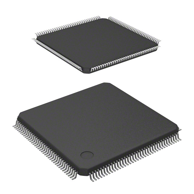


 工商网监
湘ICP备2023018690号
工商网监
湘ICP备2023018690号
