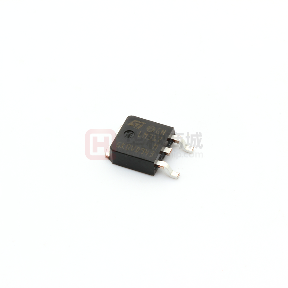
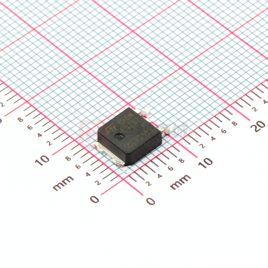
LM217M LM317M
Medium current 1.2 to 37 V adjustable voltage regulator
Features
■ ■ ■ ■ ■ ■ ■ ■
Output voltage range: 1.2 to 37 V Output current in excess of 500 mA Line regulation typ. 0.01 % Load regulation typ. 0.1 % Thermal overload protection Short circuit protection Output transition safe area compensation Floating operation for high voltage applications exceptionally easy to use and eliminating the stocking of many fixed regulators.
TO-220 DPAK
Description
The LM217M/LM317M are monolithic integrated circuits in TO-220 and DPAK packages intended for use as positive adjustable voltage regulators. They are designed to supply until 500 mA of load current with an output voltage adjustable over a 1.2 to 37 V range. The nominal output voltage is selected by means of only a resistive divider, making the device
Table 1.
Device summary
Order codes TO-220 DPAK (tape and reel) LM217MDT-TR LM317MT LM317MDT-TR
February 2008
Rev 7
1/21
www.st.com 21
�Contents
LM217M - LM317M
Contents
1 2 3 4 5 6 Diagram . . . . . . . . . . . . . . . . . . . . . . . . . . . . . . . . . . . . . . . . . . . . . . . . . . . 3 Pin configuration . . . . . . . . . . . . . . . . . . . . . . . . . . . . . . . . . . . . . . . . . . . 4 Maximum ratings . . . . . . . . . . . . . . . . . . . . . . . . . . . . . . . . . . . . . . . . . . . . 5 Electrical characteristics . . . . . . . . . . . . . . . . . . . . . . . . . . . . . . . . . . . . . 6 Typical performance . . . . . . . . . . . . . . . . . . . . . . . . . . . . . . . . . . . . . . . . . 8 Application information . . . . . . . . . . . . . . . . . . . . . . . . . . . . . . . . . . . . . . 9
6.1 6.2 6.3 External capacitors (Figure 8) . . . . . . . . . . . . . . . . . . . . . . . . . . . . . . . . . . 9 Protection diodes (Figure 8) . . . . . . . . . . . . . . . . . . . . . . . . . . . . . . . . . . . . 9 Start-up block . . . . . . . . . . . . . . . . . . . . . . . . . . . . . . . . . . . . . . . . . . . . . . . 9
7 8 9
Application circuits . . . . . . . . . . . . . . . . . . . . . . . . . . . . . . . . . . . . . . . . . 10 Package mechanical data . . . . . . . . . . . . . . . . . . . . . . . . . . . . . . . . . . . . 12 Revision history . . . . . . . . . . . . . . . . . . . . . . . . . . . . . . . . . . . . . . . . . . . 20
2/21
�LM217M - LM317M
Diagram
1
Figure 1.
Diagram
Schematic diagram
3/21
�Pin configuration
LM217M - LM317M
2
Figure 2.
Pin configuration
Pin connections (top view)
TO-220
DPAK
4/21
�LM217M - LM317M
Maximum ratings
3
Table 2.
Symbol VI-VO PD TOP TSTG
Maximum ratings
Absolute maximum ratings
Parameter Input-output differential voltage Power dissipation Operating junction temperature range (1) Storage temperature range for LM217M for LM317M Value 40 Internally limited -40 to 125 °C 0 to 125 -55 to 150 °C Unit V mW
1. Re-Boot is not guaranteed for TJ ≥ 85°C.
Table 3.
Symbol RthJC RthJA
Thermal data
Parameter Thermal resistance junction-case Thermal resistance junction-ambient TO-220 3 50 DPAK 8 100 Unit °C/W °C/W
Figure 3.
Test circuit
5/21
�Electrical characteristics
LM217M - LM317M
4
Table 4.
Symbol ΔVO
Electrical characteristics
Electrical characteristics of LM217M (refer to the test circuits, TJ = - 40 to 125 °C, VI - VO = 5 V, IO = 100 mA, PD ≤ 7.5 W, unless otherwise specified)
Parameter Line regulation Test conditions VI - VO = 3 to 40 V VO ≤5 V IO = 10 to 500mA Load regulation VO ≥ 5 V IO = 10 to 500mA Adjustment pin current Adjustment pin current Reference voltage Output voltage temperature stability Minimum load current Maximum output current Output noise voltage (percentage of VO) Supply voltage rejection (1) VI - VO = 40 V VI - VO ≤15 V VI - VO = 40 V, Pd < PDMAX, TJ = 25°C B = 10 Hz to 100 kHz, TJ = 25°C TJ = 25°C f = 120 Hz CADJ = 0 CADJ = 10 µF 66 500 VI - VO = 3 to 40 V, IO = 10 to 500 mA VI - VO = 3 to 40 V, IO = 10 to 500 mA 1.2 TJ = 25°C 0.1 0.3 50 0.2 1.25 0.7 3.5 1000 mA 200 0.003 65 dB 80 % 5 0.3 1 100 5 1.3 %/VO µA µA V % mA TJ = 25°C Min. Typ. 0.01 0.02 TJ = 25°C 5 20 Max. 0.02 %/V 0.05 15 mV 50 Unit
ΔVO
IADJ ΔIADJ VREF ΔVO/VO IO(min) IO(max) eN
SVR
1. CADJ is connected between Adjust pin and Ground.
6/21
�LM217M - LM317M Table 5.
Symbol ΔVO
Electrical characteristics
Electrical characteristics of LM317M (refer to the test circuits, TJ = 0 to 125 °C, VI - VO = 5 V, IO = 100 mA, PD ≤ 7.5 W, unless otherwise specified)
Parameter Line regulation Test conditions VI - VO = 3 to 40 V VO ≤5 V IO = 10 to 500mA Load regulation VO ≥ 5 V IO = 10 to 500mA Adjustment pin current Adjustment pin current Reference voltage Output voltage temperature stability Minimum load current Maximum output current Output noise voltage (percentage of VO) Supply voltage rejection (1) VI - VO = 40 V VI - VO ≤15 V VI - VO = 40 V, Pd < PDMAX, TJ = 25°C B = 10 Hz to 100 kHz, TJ = 25°C TJ = 25°C f = 120 Hz CADJ = 0 CADJ = 10 µF 66 500 VI - VO = 3 to 40 V, IO = 10 to 500 mA VI - VO = 3 to 40 V, IO = 10 to 500 mA 1.2 TJ = 25°C 0.1 0.3 50 0.2 1.25 0.7 3.5 1000 mA 200 0.003 65 dB 80 % 10 0.5 1.5 100 5 1.3 %/VO µA µA V % mA TJ = 25°C Min. Typ. 0.01 0.02 TJ = 25°C 5 20 Max. 0.04 %/V 0.07 25 mV 70 Unit
ΔVO
IADJ ΔIADJ VREF ΔVO/VO IO(min) IO(max) eN
SVR
1. CADJ is connected between Adjust pin and Ground.
7/21
�Typical performance
LM217M - LM317M
5
Figure 4.
Typical performance
Current limit Figure 5. Minimum operating current
Figure 6.
Basic adjustable regulator
Figure 7.
Thermal resistance & maximum power dissipation vs P.C.B. copper length for DPAK
Note:
8/21
Pdmax calculated for Ta = 50°C.
�LM217M - LM317M
Application information
6
Application information
The LM217M/LM317M provide an internal reference voltage of 1.25 V between the output and adjustment terminals. These devices are used to set a constant current flow across an external resistor divider (see Figure 6), giving an output voltage VO of: VO = VREF (1 + R2 / R1) + IADJ R2. The devices were designed to minimize the term IADJ (100 µA max) and to maintain it very constant in line and load changes. Usually, the error term IADJ × R2 can be neglected. To obtain the previous requirement, all the regulator quiescent current is returned to the output terminal, imposing a minimum load current condition. If the load is insufficient, the output voltage will rise. Since the LM217M/LM317M devices are floating regulators and "see" only the input-tooutput differential voltage, supplies of very high voltage with respect to ground can be regulated as long as the maximum input-to-output differential is not exceeded. Furthermore, programmable regulators are easily obtained and, by connecting a fixed resistor between the adjustment and output, the devices can be used as a precision current regulator. In order to optimize the load regulation, the current set resistor R1 (see Figure 6) should be tied as close as possible to the regulator, while the ground terminal of R2 should be near the ground of the load to provide remote ground sensing.
6.1
External capacitors (Figure 8)
Normally no capacitors are needed unless the devices are situated far from the input filter capacitors; in which case an input bypass is needed. A 0.1 µF disc or 1 µF tantalum input bypass capacitor (CI) is recommended to reduce the sensitivity to input line impedance. The adjustment terminal may be bypassed to ground to improve ripple rejection. This capacitor (CADJ) prevents ripple from being amplified as the output voltage is increased. A 10 µF capacitor should improve ripple rejection of about 80 dB at 120 Hz in a 10 V application. Although the LM217M/LM317M devices are stable with no output capacitance like any feedback circuit, certain values of external capacitance can cause excessive ringing. An output capacitance (CO) in the form of a 1 µF tantalum or 25 µF aluminium electrolytic capacitor on the output swamps this effect and insures stability.
6.2
Protection diodes (Figure 8)
When external capacitors are used with any IC regulator it is sometimes necessary to add protection diodes to prevent the capacitors from discharging through low current points into the regulator. Figure 6 shows the LM217M/LM317M with the recommended protection diodes for output voltages in excess of 25 V or high capacitance values (C3 > 25 µF, C2 > 10 µF). Diode D1 prevents C3 from discharging through the IC during an input short-circuit. The combination of diodes D1 and D2 prevents C2 from discharging through the regulator during an input or output short-circuit.
6.3
Start-up block
It’s not guaranteed the Re-Boot of the device when the junction temperature is over 85 °C.
9/21
�Application circuits
LM217M - LM317M
7
Figure 8.
Application circuits
Voltage regulator with protection diodes
Figure 9.
Slow turn-on 15 V regulator
Figure 10. Current regulator
IO=VREF/R1 + IADJ = 1.25V/R1
10/21
�LM217M - LM317M
Application circuits
Figure 11. 5 V electronic shut-down regulator
Figure 12. Digitally selected outputs
(R2 = sets maximum VO)
11/21
�Package mechanical data
LM217M - LM317M
8
Package mechanical data
In order to meet environmental requirements, ST offers these devices in ECOPACK® packages. These packages have a lead-free second level interconnect. The category of second Level Interconnect is marked on the package and on the inner box label, in compliance with JEDEC Standard JESD97. The maximum ratings related to soldering conditions are also marked on the inner box label. ECOPACK is an ST trademark. ECOPACK specifications are available at: www.st.com.
12/21
�LM217M - LM317M
Package mechanical data
TO-220 mechanical data
Dim. A C D D1 E F F1 F2 G G1 H2 L2 L4 L5 L6 L7 L9 DIA. 13.0 2.65 15.25 6.2 3.5 3.75 0.49 0.61 1.14 1.14 4.95 2.4 10.0 16.4 14.0 2.95 15.75 6.6 3.93 3.85 0.511 0.104 0.600 0.244 0.137 0.147 mm. Min. 4.40 1.23 2.40 1.27 0.70 0.88 1.70 1.70 5.15 2.7 10.40 0.019 0.024 0.044 0.044 0.194 0.094 0.393 0.645 0.551 0.116 0.620 0.260 0.154 0.151 Typ. Max. 4.60 1.32 2.72 Min. 0.173 0.048 0.094 0.050 0.027 0.034 0.067 0.067 0.203 0.106 0.409 inch. Typ. Max. 0.181 0.051 0.107
P011C
13/21
�Package mechanical data
LM217M - LM317M
Figure 13. Drawing dimension DPAK (type STD-ST)
0068772/G
14/21
�LM217M - LM317M
Package mechanical data
Figure 14. Drawing dimension DPAK (type FUJITSU-Subcon.)
0068772/G
15/21
�Package mechanical data
LM217M - LM317M
Figure 15. Drawing dimension DPAK (type IDS-Subcon.)
0068772/G
16/21
�LM217M - LM317M
Package mechanical data
Table 6.
DPAK mechanical data
type STD-ST type FUJITSU-Subcon. mm. Max. 2.40 1.10 0.23 0.90 5.40 0.60 0.60 6.20 5.10 6.40 4.70 2.28 4.40 9.35 1.00 2.80 0.80 0.60 0.20 0° 8° 0° 1.00 1.03 0.70 0.40 8° 0° 1.13 0.90 4.60 10.10 9.90 1.40 10.30 1.60 2.23 6.60 Min. 2.25 0.96 0 0.76 5.28 0.46 0.46 6.05 5.27 6.55 6.60 4.77 2.28 2.33 4.51 9.40 0.90 2.50 0.89 0.64 0.20 8° 2.65 1.27 1.02 Typ. 2.30 Max. 2.35 1.06 0.10 0.86 5.38 0.56 0.56 6.15 5.47 6.65 6.35 4.70 2.28 4.61 10.42 Min. 2.19 0.89 0.03 0.64 5.21 0.46 0.46 5.97 5.20 6.73 type IDS-Subcon mm. Typ. Max. 2.38 1.14 0.23 0.88 5.46 0.58 0.58 6.22
Dim. Min. A A1 A2 b b4 c c2 D D1 E E1 e e1 H L L1 L2 L4 R V2 2.20 0.90 0.03 0.64 5.20 0.45 0.48 6.00
mm. Typ.
Note:
The DPAK package coming from the two subcontractors (Fujitsu and IDS) are fully compatible with the ST's package suggested footprint.
17/21
�Package mechanical data
LM217M - LM317M
Figure 16. DPAK footprint recommended data
Table 7.
Footprint data
Values Dim. A B C D E F G mm. 6.70 6.70 1.8 3.0 1.60 2.30 2.30 inch. 0.264 0.64 0.070 0.118 0.063 0.091 0.091
18/21
�LM217M - LM317M
Package mechanical data
Tape & reel DPAK-PPAK mechanical data
mm. Dim. Min. A C D N T Ao Bo Ko Po P 6.80 10.40 2.55 3.9 7.9 6.90 10.50 2.65 4.0 8.0 12.8 20.2 60 22.4 7.00 10.60 2.75 4.1 8.1 0.268 0.409 0.100 0.153 0.311 0.272 0.413 0.104 0.157 0.315 13.0 Typ. Max. 330 13.2 0.504 0.795 2.362 0.882 0.2.76 0.417 0.105 0.161 0.319 0.512 Min. Typ. Max. 12.992 0.519 inch.
19/21
�Revision history
LM217M - LM317M
9
Table 8.
Date
Revision history
Document revision history
Revision 5 6 7 Changes The document has been reformatted. DPAK mechanical data updated, added footprint data. Added: Table 1 on page 1.
21-Jun-2004 06-Dec-2006 11-Feb-2008
20/21
�LM217M - LM317M
Please Read Carefully:
Information in this document is provided solely in connection with ST products. STMicroelectronics NV and its subsidiaries (“ST”) reserve the right to make changes, corrections, modifications or improvements, to this document, and the products and services described herein at any time, without notice. All ST products are sold pursuant to ST’s terms and conditions of sale. Purchasers are solely responsible for the choice, selection and use of the ST products and services described herein, and ST assumes no liability whatsoever relating to the choice, selection or use of the ST products and services described herein. No license, express or implied, by estoppel or otherwise, to any intellectual property rights is granted under this document. If any part of this document refers to any third party products or services it shall not be deemed a license grant by ST for the use of such third party products or services, or any intellectual property contained therein or considered as a warranty covering the use in any manner whatsoever of such third party products or services or any intellectual property contained therein.
UNLESS OTHERWISE SET FORTH IN ST’S TERMS AND CONDITIONS OF SALE ST DISCLAIMS ANY EXPRESS OR IMPLIED WARRANTY WITH RESPECT TO THE USE AND/OR SALE OF ST PRODUCTS INCLUDING WITHOUT LIMITATION IMPLIED WARRANTIES OF MERCHANTABILITY, FITNESS FOR A PARTICULAR PURPOSE (AND THEIR EQUIVALENTS UNDER THE LAWS OF ANY JURISDICTION), OR INFRINGEMENT OF ANY PATENT, COPYRIGHT OR OTHER INTELLECTUAL PROPERTY RIGHT. UNLESS EXPRESSLY APPROVED IN WRITING BY AN AUTHORIZED ST REPRESENTATIVE, ST PRODUCTS ARE NOT RECOMMENDED, AUTHORIZED OR WARRANTED FOR USE IN MILITARY, AIR CRAFT, SPACE, LIFE SAVING, OR LIFE SUSTAINING APPLICATIONS, NOR IN PRODUCTS OR SYSTEMS WHERE FAILURE OR MALFUNCTION MAY RESULT IN PERSONAL INJURY, DEATH, OR SEVERE PROPERTY OR ENVIRONMENTAL DAMAGE. ST PRODUCTS WHICH ARE NOT SPECIFIED AS "AUTOMOTIVE GRADE" MAY ONLY BE USED IN AUTOMOTIVE APPLICATIONS AT USER’S OWN RISK.
Resale of ST products with provisions different from the statements and/or technical features set forth in this document shall immediately void any warranty granted by ST for the ST product or service described herein and shall not create or extend in any manner whatsoever, any liability of ST.
ST and the ST logo are trademarks or registered trademarks of ST in various countries. Information in this document supersedes and replaces all information previously supplied. The ST logo is a registered trademark of STMicroelectronics. All other names are the property of their respective owners.
© 2008 STMicroelectronics - All rights reserved STMicroelectronics group of companies Australia - Belgium - Brazil - Canada - China - Czech Republic - Finland - France - Germany - Hong Kong - India - Israel - Italy - Japan Malaysia - Malta - Morocco - Singapore - Spain - Sweden - Switzerland - United Kingdom - United States of America www.st.com
21/21
�


 工商网监
湘ICP备2023018690号
工商网监
湘ICP备2023018690号
