PD54003L-E
RF Power Transistors The LdmoST Plastic FAMILY
Features
■ ■ ■ ■ ■ ■ ■
EXCELLENT THERMAL STABILITY COMMON SOURCE CONFIGURATION POUT = 3W WITH 20 dB GAIN @ 500MHz NEW RF PLASTIC PACKAGE EDS PROTECTION SUPPLIED IN TAPE & REEL OF 3K UNITS IN COMPLIANCE WITH THE 2002/93/EC EUROPEAN DIRECTIVE
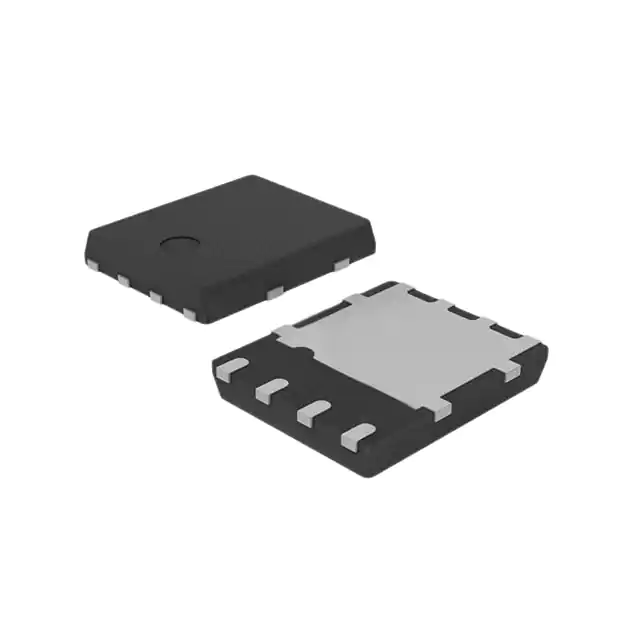
PowerFLAT™ (5x5)
Description
The PD54003L-E is a common source N-Channel, enhancement-mode lateral FieldEffect RF power transistor. It is designed for high gain, broad band commercial and industrial applications. It operates at 7 V in common source mode at frequencies of up to 1 GHz. PD54003L-E boasts the excellent gain, linearity and reliability of STH1LV latest LDMOS technology mounted in the innovative leadless SMD plastic package, PowerFLAT™. PD54003L-E’s superior linearity performance makes it an ideal solution for portable radio.
Pin Connection
TOP VIEW
Order Codes
Part Number PD54003L-E Marking 54003 Package PowerFLAT (5x5) Packaging Tape & Reel
January 2006
Rev 1 1/13
www.st.com 13
�PD54003L-E
Contents
1 Electrical Data . . . . . . . . . . . . . . . . . . . . . . . . . . . . . . . . . . . . . . . . . . . . . . . . 3
1.1 1.2 1.3 Maximum Ratings . . . . . . . . . . . . . . . . . . . . . . . . . . . . . . . . . . . . . . . . . . . . . . 3 Thermal Data . . . . . . . . . . . . . . . . . . . . . . . . . . . . . . . . . . . . . . . . . . . . . . . . . 3 Electrical Characteristics . . . . . . . . . . . . . . . . . . . . . . . . . . . . . . . . . . . . . . . . . 4
2
Typical Performance . . . . . . . . . . . . . . . . . . . . . . . . . . . . . . . . . . . . . . . . . . . 5
2.1 Typical Performance (Broadband) . . . . . . . . . . . . . . . . . . . . . . . . . . . . . . . . . 7
3 4
Package Mechanical Data . . . . . . . . . . . . . . . . . . . . . . . . . . . . . . . . . . . . . . . 8 Revision History . . . . . . . . . . . . . . . . . . . . . . . . . . . . . . . . . . . . . . . . . . . . . 12
2/13
�PD54003L-E
1 Electrical Data
1
1.1
Table 1.
Electrical Data
Maximum Ratings
Absolute Maximum Ratings (TCASE = 25°C)
Symbol V(BR)DSS VGS ID PDISS TJ TSTG Drain Source Voltage Gate-Source Voltage Drain Current
Parameter
Value 25 -0.5 to +15 4 19.5 150 -65 to +150
Unit V V A W °C °C
Power Dissipation (tcase=70°C) Max. Operating Junction Temperature Storage Temperature
1.2
Table 2.
Thermal Data
Thermal data
Parameter Junction to Case thermal resistance Value 4.1 Unit °C/W
Symbol RthJC
3/13
�1 Electrical Data
PD54003L-E
1.3
Electrical Characteristics
(TCASE = 25°C)
Table 3.
Symbol IDSS IGSS VGS(Q) VDS(ON) gFS CISS COSS CRSS
Static
Test Conditions VGS = 0 V VGS = 20 V VDS = 10 V VGS = 10 V VDS = 10 V VGS = 0 V VGS = 0 V VGS = 0 V VDS = 25 V VDS = 0 V ID = 50 mA ID = 0.5 A ID = 3.2 A VDS = 7.5 V VDS = 7.5 V VDS = 7.5 V f = 1 MHz f = 1 MHz f = 1 MHz 2.0 0.13 TBD 54 43 4.0 Min. Typ. Max. 1 1 3.3 0.16 Unit μA μA V V mho pF pF pF
Table 4.
Symbol POUT G PS ηD Load Mismatch
Dynamic
Test Conditions VDD = 7.5 V VDD = 7.5 V VDD = 7.5 V VDD = 9.5 V IDQ = 50 mA f = 500MHz f = 500MHz f = 500MHz f = 500MHz Min. 3 16 50 20:1 20 55 Typ. Max. Unit W dB % VSWR
IDQ = 50 mA POUT = 3 W IDQ = 50 mA POUT = 3 W
IDQ = 50 mA POUT = 3W All Phase Angles
Table 5.
ESD Protection Characteristics
Test Conditions Human Body Model Machine Model Class 2 M3
Table 6.
Moisture Sensitivy Level
Test Methodology J-STD-020B Rating MSL 3
4/13
�PD54003L-E
2 Typical Performance
2
Typical Performance
Capacitance vs. Supply Voltage Figure 2. Output Power vs. Input Power
Figure 1.
1000
5
4
100 C (pF) Ciss
f = 500 MHz
Coss
Pout (W)
Crss
3
2
10
1 Vds = 7.5 V Idq= 50 mA
1 0 2 4 6 8 Vds (V) 10 12 14 16
0 0 5 10 15 20 25 30 35 40 45 50 55 60 Pin (mW)
Figure 3.
Power Gain vs. Output Power
Figure 4.
Efficiency vs Output Power
5
26 24 22 20 18 16 Gp (dB) 14 12 10 8 6 4 2 0 0 1 2 Pout (W) 3 4 5 Vds = 7.5 V Idq = 50 mA
4
f = 500 MHz
Pout (W)
f = 500 MHz
3
2
1 Vds = 7.5 V Idq= 50 mA 0 0 5 10 15 20 25 30 35 40 45 50 55 60 Pin (mW)
Figure 5.
Output Power vs Bias Current
4
3 Pout (W)
f = 500 MHz
2
1 Vds = 7.5 V Pin= 15 dBm 0 0 50 100 150 200 250 Idq (mA) 300 350 400 450 500
5/13
�2 Typical Performance
PD54003L-E
Figure 7. Output Power vs Supply Voltage
Figure 6.
Efficiency vs Bias Current
70
8 7 6
60
Nd (%)
50
f = 500 MHz
40
Pout (W)
5 4 3 2
30
20 Vds = 7.5 V P in= 15 dBm 10 0 50 100 150 200 250 Idq (mA) 300 350 400 450 500
1 0 5 6 7 Vds (V) 8
Idq = 50 mA Pin = 15 dBm f = 500 MHz
9
10
Figure 8.
Output Power vs Gate-Source Volt
4 Pin = 15 dBm Vdd = 7.5 V f = 500 MHz 3
Pout (W)
2
1
0 0.0 0.5 1.0 1.5 Vgs (V) 2.0 2.5 3.0
6/13
�PD54003L-E
2 Typical Performance
2.1
Typical Performance (Broadband)
Power Gain vs Frequency Figure 10. Efficiency vs Frequency
Figure 9.
20 18
70
60
16 14 Gp (dB)
Nd (%) 50
12 10 8 6 4 2 0 460 Vds = 7.5 V Idq = 50 mA Pout= 3 W 470 480 490 500 f (MHz) 510 520 530 540
40
30
20 Vds = 7.5 V Iqd = 50 mA Pout = 3 W 470 480 490 500 f (MHz) 510 520 530 540
10
0 460
Figure 11. Return Loss vs Frequency
0
-5
RL (dB)
-10
-15
-20 Vds = 7.5 V Idq = 50 mA Pout = 3 W -25 460 470 480 490 500 f (MHz) 510 520 530 540
7/13
�3 Package Mechanical Data
PD54003L-E
3
Package Mechanical Data
In order to meet environmental requirements, ST offers these devices in ECOPACK® packages. These packages have a Lead-free second level interconnect . The category of second level interconnect is marked on the package and on the inner box label, in compliance with JEDEC Standard JESD97. The maximum ratings related to soldering conditions are also marked on the inner box label. ECOPACK is an ST trademark. ECOPACK specifications are available at: www.st.com
8/13
�PD54003L-E
Table 7.
Dim. MIN. A A1 A3 AA b c D d E E2 e f g h 2.49 0.15 0.43 0.64 TYP. 0.90 0.02 0.24 0.25 0.51 0.71 5.00 0.30 5.00 2.57 1.27 3.37 0.74 0.21 2.64 0.098 0.35 0.58 0.79 0.006 0.017 0.025 MAX. 1.00 0.05 MIN. TYP. 0.035 0.001 0.009 0.01 0.020 0.028 0.197 0.011 0.197 0.101 0.050 0.132 0.03 0.008
3 Package Mechanical Data
PowerFLAT™ Mechanical Data
mm inch MAX. 0.039 0.002
0.014 0.023 0.031
0.104
Figure 12. PowerFLAT™ Package Dimensions
9/13
�3 Package Mechanical Data
PD54003L-E
Table 8.
DIM.
PowerFLAT™ Tape & Reel Dimensions
mm. MIN. TYP 5.25 5.25 1.1 MAX. 5.35 5.35 1.2
Ao Bo Ko
5.15 5.15 1.0
Figure 13. PowerFLAT™ Tape & Reel
10/13
�PD54003L-E
Table 9. Recommended FOOTPRINT
3 Package Mechanical Data
11/13
�4 Revision History
PD54003L-E
4
Revision History
Date 04-Jan-2006 Revision 1 First Issue. Description of Changes
12/13
�PD54003L-E
4 Revision History
Information furnished is believed to be accurate and reliable. However, STMicroelectronics assumes no responsibility for the consequences of use of such information nor for any infringement of patents or other rights of third parties which may result from its use. No license is granted by implication or otherwise under any patent or patent rights of STMicroelectronics. Specifications mentioned in this publication are subject to change without notice. This publication supersedes and replaces all information previously supplied. STMicroelectronics products are not authorized for use as critical components in life support devices or systems without express written approval of STMicroelectronics. The ST logo is a registered trademark of STMicroelectronics. All other names are the property of their respective owners © 2006 STMicroelectronics - All rights reserved STMicroelectronics group of companies Australia - Belgium - Brazil - Canada - China - Czech Republic - Finland - France - Germany - Hong Kong - India - Israel - Italy - Japan Malaysia - Malta - Morocco - Singapore - Spain - Sweden - Switzerland - United Kingdom - United States of America www.st.com
13/13
�
很抱歉,暂时无法提供与“PD54003L-E”相匹配的价格&库存,您可以联系我们找货
免费人工找货