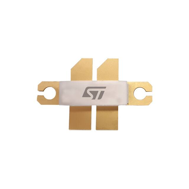
RF2L16180CB4
Datasheet
180 W, 28 V, 1.3 to 1.6 GHz RF power LDMOS transistor
Features
1
2
5
4
3
B4E
Pin connection
Pin
Connection
1
Drain A
2
Drain B
3
Source (bottom side)
4
Gate B
5
Gate A
•
•
•
•
•
•
Order code
f (MHz)
VDD
POUT
Gain
Efficiency
RF2L16180CB4
1450
28 V
180 W
14 dB
60%
High efficiency and linear gain operations
Integrated ESD protection
Internally matched for ease of use
Optimized for Doherty applications
Large positive and negative gate-source voltage range for improved class C
operation
In compliance with the European Directive 2002/95/EC
Applications
•
•
Multicarrier base station
Industrial, scientific and medical
Description
The RF2L16180CB4 is 180 W, 28 V internally matched LDMOS transistor designed
for multicarrier WCDMA/PCS/DCS/LTE base station and ISM applications with
frequencies from 1300 to 1600 MHz. Four leads can be configured as single ended,
180 degree push-pull or 90 degree hybrid or Doherty with proper external matching
network.
Product status link
RF2L16180CB4
Product summary
Order code
RF2L16180CB4
Marking
2L16180
Package
B4E
Packing
Tape and reel 13”
Base/bulk
Quantity
120/120
DS13287 - Rev 2 - April 2021
For further information contact your local STMicroelectronics sales office.
www.st.com
�RF2L16180CB4
Electrical ratings
1
Electrical ratings
Table 1. Absolute maximum ratings (TC= 25 °C)
Symbol
Parameter
Value
Unit
V(BR)DSS
Drain-source voltage
65
V
VGS
Gate-source voltage
-6 to 10
V
VDD
Maximum operating voltage
32
V
TSTG
Storage temperature range
-65 to 150
°C
200
°C
Value
Unit
0.38
°C/W
TJ
Maximum junction temperature
Table 2. Thermal data
Symbol
RthJC(1)
Parameter
Thermal resistance, junction-to-case
1. TC = 85 °C , TJ = 200 °C, DC test.
Table 3. ESD protection
Symbol
DS13287 - Rev 2
Test methodology
Class
HBM
Human body model (according to ANSI/ESDA/JEDEC JS001-2017)
1C
CDM
Charge device model (according to ANSI/ESDA/JEDEC JS-002-2014)
C3
page 2/12
�RF2L16180CB4
Electrical characteristics
2
Electrical characteristics
TC = 25 °C unless otherwise specified.
Table 4. Static (per side)
Symbol
V(BR)DSS
Parameter
Drain-source breakdown voltage
Test conditions
VGS = 0 V, IDS = 100 μA
Min.
Typ.
Max.
65
Unit
V
VGS = 0 V, VDS = 28 V
IDSS
Zero-gate voltage drain current
IGSS
Gate-body leakage current
VGS=-6/10 V, VDS=0 V
VGS(th)
Gate threshold voltage
VDS = 28 V, IDS = 600 μA
1.5
2.5
VGS(Q)
Gate quiescent voltage
VDS= 28 V, IDS = 100 mA
1.5
4
VDS(on)
Static drain-source on-voltage
VGS = 10 V, IDS = 3 A
RDS(on)
Drain-source on-state resistance
IDS(on)
Static drain-source on-current
VGS = 0 V, VDS = 50 V
1
μA
±100
nA
V
0.5
VGS= 10 V, VDS=100 mV
1
Ω
2.5
A
Max.
Unit
1.6
GHz
Table 5. Dynamic
Symbol
f
DS13287 - Rev 2
Test conditions
Frequency
POUT
Output power
GPS
Power gain
ƞD
Note:
Parameter
Drain efficiency
Min.
Typ.
1.3
f = 1450 MHz at 1dB compression
point in Doherty amplifier test
circuit, pulsed CW
180
W
14
dB
60
%
VDD = 28 V, IDQMain = 600 mA, VGpeak = 0.9 V, pulse width = 10 µs, duty cycle = 12%.
page 3/12
�RF2L16180CB4
Typical performance
3
Typical performance
Table 6. Output power, power gain and drain efficiency vs input power (f = 1450 MHz)
PIN (dBm)
POUT (dBm)
POUT (W)
IDS (A)
GPS (dB)
ηD(%)
24.6
39.8
9.5
1.3
15.2
25.7
25.6
40.8
12.1
1.5
15.2
29.2
26.6
41.9
15.4
1.7
15.3
33.0
27.6
43.0
19.9
1.9
15.4
36.9
28.6
44.1
25.6
2.2
15.5
40.8
29.6
45.2
33.0
2.7
15.6
44.2
30.6
46.3
42.6
3.2
15.7
47.3
31.6
47.3
53.9
3.9
15.7
49.9
32.6
48.3
67.2
4.6
15.7
51.9
33.5
49.2
82.3
5.5
15.6
53.6
34.5
49.9
96.6
6.2
15.3
55.3
35.5
50.7
116.5
7.3
15.2
57.0
36.5
51.3
135.6
8.3
14.8
58.2
37.4
51.9
154.8
9.2
14.5
60.2
38.4
52.4
172.9
10.1
14.0
61.4
39.3
52.8
188.9
10.8
13.4
62.5
40.2
53.0
200.6
11.4
12.9
63.1
41.1
53.3
213.1
12.0
12.2
63.7
16
70
15
60
14
50
13
40
12
30
11
20
40
41
42
43
Power gain
44
45
46
47
48
49
50
51
DS13287 - Rev 2
52
53
54
POUT (dbm)
Efficiency
Note:
Drain efficiency, ηD (%)
Power gain, GPS (dB)
Figure 1. Power Gain and drain efficiency vs output power at 1450 MHz (on Doherty test fixture)
GADG110620201522MT
VDD = 28 V, IDQMain = 600 mA, pulsed CW, pulse width = 10 μs, duty cycle = 12%
page 4/12
�RF2L16180CB4
Test circuits
4
Test circuits
Figure 2. Test circuit layout
DS13287 - Rev 2
page 5/12
�RF2L16180CB4
Test circuits
Figure 3. Test circuit photo
2L16180
Table 7. Component list
Component
Value
Size
Reference
C2, C8, C13, C18
Ceramic capacitor, 28 pF
0805
ATC600F
C3, C16
Ceramic capacitor, 3.3 pF
0805
ATC600F
C4, C7, C11, C19
Ceramic capacitor, 5.6 pF
0805
ATC600F
C5
Ceramic capacitor, 0.7 pF
0805
ATC600F
C6, C14, C15, C17
Ceramic capacitor, 2.7 pF
0805
ATC600F
C12
Ceramic capacitor, 1.0 pF
0805
ATC600F
C1, C9, C10, C20
10 μF
1210
100 V ceramic multilayer
capacitor
C21, C22
220 μF
63 V electrolytic capacitor
D1
R1
50 Ω
0805
4 W chip resistor
R2, R3
10 Ω
0805
Chip resistor
PCB
DS13287 - Rev 2
Spliter
0.508 mm [0.020''] thick, ԑr = 3.48, Rogers RO4350B, 1 oz. copper
page 6/12
�RF2L16180CB4
Package information
5
Package information
In order to meet environmental requirements, ST offers these devices in different grades of ECOPACK packages,
depending on their level of environmental compliance. ECOPACK specifications, grade definitions and product
status are available at: www.st.com. ECOPACK is an ST trademark.
5.1
B4E package information
Figure 4. B4E package outline
DM00418520_2
DS13287 - Rev 2
page 7/12
�RF2L16180CB4
B4E package information
Table 8. B4E package mechanical data
Dim.
DS13287 - Rev 2
mm
Min.
Typ.
Max.
A
27.81
27.94
28.07
B
18.93
19.43
19.93
C
33.91
34.04
34.17
D
9.65
9.78
9.91
E
19.56
19.81
20.06
F
3.23
3.61
3.99
G
1.40
1.53
1.66
H
0.07
L
9.20
9.40
9.60
M
4.67
4.80
4.93
N
0.89
1.02
1.15
O
4.70
4.83
4.96
P
3.13
3.26
3.39
Q
7.77
7.90
8.03
0.15
R
0.50
R1
1.52
R2
1.63
CH1
2.72
page 8/12
�RF2L16180CB4
Marking information
6
Marking information
Figure 5. Marking composition
PACKAGE FACE : TOP
LEGEND
Unmarkable Surface
Marking Composition Field
A - STANDARD ST LOGO
B - ECO level
(e4)
A
C - MARKING AREA
D - ADDITIONAL
INFORMATION
B
(MAX CHAR ALLOWED = 7)
E - COUNTRY OF ORIGIN
C
(MAX CHAR ALLOWED = 3)
F - Assy Plant
D
E
F
G
H
(PP)
G - Assy Year
(Y)
H - Assy Week
(WW)
GADG040220211644GT
DS13287 - Rev 2
page 9/12
�RF2L16180CB4
Revision history
Table 9. Document revision history
Date
Version
02-Jul-2020
1
Changes
First release.
Modified marking on cover page.
Modified Table 1. Absolute maximum ratings (TC= 25 °C), Table 2. Thermal
data, Table 3. ESD protection.
21-Apr-2021
2
Modified Table 4. Static (per side).
Modified Figure 1. Power Gain and drain efficiency vs output power at 1450
MHz (on Doherty test fixture).
Added Section 6 Marking information.
Minor text changes.
DS13287 - Rev 2
page 10/12
�RF2L16180CB4
Contents
Contents
1
Electrical ratings . . . . . . . . . . . . . . . . . . . . . . . . . . . . . . . . . . . . . . . . . . . . . . . . . . . . . . . . . . . . . . . . . .2
2
Electrical characteristics. . . . . . . . . . . . . . . . . . . . . . . . . . . . . . . . . . . . . . . . . . . . . . . . . . . . . . . . . . . 3
3
Typical performance . . . . . . . . . . . . . . . . . . . . . . . . . . . . . . . . . . . . . . . . . . . . . . . . . . . . . . . . . . . . . . . 4
4
Test circuits . . . . . . . . . . . . . . . . . . . . . . . . . . . . . . . . . . . . . . . . . . . . . . . . . . . . . . . . . . . . . . . . . . . . . . .5
5
Package information. . . . . . . . . . . . . . . . . . . . . . . . . . . . . . . . . . . . . . . . . . . . . . . . . . . . . . . . . . . . . . .7
5.1
6
B4E package information . . . . . . . . . . . . . . . . . . . . . . . . . . . . . . . . . . . . . . . . . . . . . . . . . . . . . . . . 7
Marking information . . . . . . . . . . . . . . . . . . . . . . . . . . . . . . . . . . . . . . . . . . . . . . . . . . . . . . . . . . . . . . . 9
Revision history . . . . . . . . . . . . . . . . . . . . . . . . . . . . . . . . . . . . . . . . . . . . . . . . . . . . . . . . . . . . . . . . . . . . . . .10
DS13287 - Rev 2
page 11/12
�RF2L16180CB4
IMPORTANT NOTICE – PLEASE READ CAREFULLY
STMicroelectronics NV and its subsidiaries (“ST”) reserve the right to make changes, corrections, enhancements, modifications, and improvements to ST
products and/or to this document at any time without notice. Purchasers should obtain the latest relevant information on ST products before placing orders. ST
products are sold pursuant to ST’s terms and conditions of sale in place at the time of order acknowledgement.
Purchasers are solely responsible for the choice, selection, and use of ST products and ST assumes no liability for application assistance or the design of
Purchasers’ products.
No license, express or implied, to any intellectual property right is granted by ST herein.
Resale of ST products with provisions different from the information set forth herein shall void any warranty granted by ST for such product.
ST and the ST logo are trademarks of ST. For additional information about ST trademarks, please refer to www.st.com/trademarks. All other product or service
names are the property of their respective owners.
Information in this document supersedes and replaces information previously supplied in any prior versions of this document.
© 2021 STMicroelectronics – All rights reserved
DS13287 - Rev 2
page 12/12
�