STB85NS04Z
STB85NS04Z-1
N-channel 11mΩ - 80A - D2PAK - I2PAK
SAFeFET™ Power MOSFET
General features
Type
VDSS
RDS(on)
ID
STB85NS04Z
Clamped
< 0.015Ω 80A(1)
STB85NS04Z-1
Clamped
< 0.015Ω 80A(1)
)
s
(
t
c
u
d
o
)
r
s
(
P
t
c
e
t
Description
u
e
d
l
o
o
r
s
P
b
Internal
schematic
diagram
e
O
t
e
l
)
o
s
(
s
t
b
c
u
O
d
o
)
r
s
P
(
t
Applications
c
e
t
u
e
l
d
o
o
r
s
P
b
OOrder codes
e
t
e
l
o
s
b
O
1. Current limited by wire bonding
3
12
■
100% avalanche tested
■
Low capacitance and gate charge
■
175°C maximum junction temperature
3
1
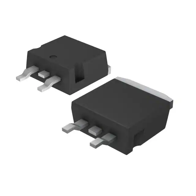
I²PAK
D²PAK
This fully clamped Power MOSFET is produced
by using the latest advanced Company’s Mesh
Overlay™ process which is based on a novel strip
layout. The inherent benefits of the new
technology coupled with the extra clamping
capabilities make this product particularly suitble
for the harshest operation conditions such as
those encountered inthe automotive environment.
Any other application requiring extra ruggedness
is also recommended.
■
Switching application
– Automotive
Part number
Marking
Package
Packaging
STB85NS04ZT4
B85NS04Z
D²PAK
Tape &reel
STB85NS04Z-1
B85NS04Z-1
I²PAK
Tube
September 2006
Rev 1
1/15
www.st.com
15
�Contents
STB85NS04Z - STB85NS04Z-1
Contents
1
Electrical ratings . . . . . . . . . . . . . . . . . . . . . . . . . . . . . . . . . . . . . . . . . . . . 3
2
Electrical characteristics . . . . . . . . . . . . . . . . . . . . . . . . . . . . . . . . . . . . . 5
2.1
3
Electrical characteristics (curves)
Test circuit
............................. 7
................................................ 9
)
s
(
t
c
u
d
o
)
r
s
(
P
t
c
e
t
u
e
d
l
o
o
r
s
P
b
e
O
t
e
l
)
o
s
(
s
t
b
c
u
O
d
o
)
r
s
P
(
t
c
e
t
u
e
l
d
o
o
r
s
P
b
O
e
t
e
l
o
s
b
O
4
Package mechanical data . . . . . . . . . . . . . . . . . . . . . . . . . . . . . . . . . . . . 10
5
Packaging mechanical data . . . . . . . . . . . . . . . . . . . . . . . . . . . . . . . . . . 13
6
Revision history . . . . . . . . . . . . . . . . . . . . . . . . . . . . . . . . . . . . . . . . . . . 14
2/15
�STB85NS04Z - STB85NS04Z-1
1
Electrical ratings
Electrical ratings
Table 1.
Absolute maximum ratings
Symbol
Parameter
Value
Unit
VDS
Drain-source voltage (VGS=0)
33 (1)
V
VGS
Gate-source voltage
± 18
V
ID
Drain current (continuous) at TC = 25°C
80 (2)
A
ID
Drain current (continuous) at TC = 100°C
60
A
)
s
(
t
c
u
d
o
)
r
s
(
P
t
c
e
t
u
e
d
l
o
o
r
s
P
b
e
O
t
e
l
)
o
s
(
s
t
b
c
u
O
d
o
)
r
s
P
(
t
c
e
t
u
e
l
d
o
o
r
s
P
b
O
e
t
e
l
o
s
b
O
IDG
Drain gate current (continuous)
± 50
mA
IGS
Gate source current (continuous)
± 50
mA
Drain current (pulsed)
320
A
Derating factor
1.43
W/°C
Total dissipation at TC = 25°C
215
W
IDM (3)
PTOT
VESD(G-S)
Gate-source ESD (HBM-C=100pF, R=1.5kΩ)
2
kV
VESD(G-D)
Gate-drain ESD (HBM-C=100pF, R=1.5kΩ)
4
kV
VESD(D-S)
Drain-source ESD (HBM-C=100pF, R=1.5kΩ)
4
kV
-55 to 175
°C
Tj
Tstg
Operating junction temperature
Storage temperature
1. Voltage is limited by zener diodes
2. Current limited by wire bonding
3. Pulse width limited by safe operating area
Table 2.
Thermal data
Value
Symbol
Parameter
Unit
D²PAK
Rthj-case
Thermal resistance junction-case max
Rthj-pcb (1) Thermal resistance junction-pcb max
Rthj-amb
Tl
I²PAK
0.7
35
°C/W
--
°C/W
Thermal resistance junction-amb max
62.5
°C/W
Maximum lead temperature for soldering
purpose
300
°C
1. When mounted on 1inch² FR-4 board, 2 oz Cu
3/15
�Electrical ratings
Table 3.
STB85NS04Z - STB85NS04Z-1
Avalanche characteristics
Symbol
Parameter
Max value
Unit
IAS
Avalanche current, repetitive or notrepetitive (pulse width limited by Tj max)
60
A
EAS
Single pulse avalanche energy
(starting Tj=25°C, ID=IAS, VDD= 30V)
550
mJ
)
s
(
t
c
u
d
o
)
r
s
(
P
t
c
e
t
u
e
d
l
o
o
r
s
P
b
e
O
t
e
l
)
o
s
(
s
t
b
c
u
O
d
o
)
r
s
P
(
t
c
e
t
u
e
l
d
o
o
r
s
P
b
O
e
t
e
l
o
s
b
O
4/15
�STB85NS04Z - STB85NS04Z-1
2
Electrical characteristics
Electrical characteristics
(TCASE=25°C unless otherwise specified)
Table 4.
Symbol
V(BR)DSS
On/off states
Parameter
Drain-source breakdown
voltage
Test conditions
ID = 1mA, VGS= 0
Min.
Typ.
Max.
33
Unit
V
VDS = 16V,
VDS = 16V, Tc=125°C
10
100
µA
µA
Gate body leakage current
(VDS = 0)
VGS = ±10V
10
µA
Gate-source breakdown
voltage
IGS = 100µA
25
V
IDSS
Zero gate voltage drain
current (VGS = 0)
IGSS
VGSS
)
s
(
t
c
u
d
o
)
r
s
(
P
t
c
e
t
u
e
d
l
o
o
r
s
P
b
e
O
t
e
l
)
o
s
(
s
t
b
c
u
O
d
o
)
r
s
P
(
t
c
e
t
u
e
l
d
o
o
r
s
P
b
O
e
t
e
l
o
s
b
O
RG
Series gate resistance
VGS(th)
Gate threshold voltage
VDS= VGS, ID = 1mA
RDS(on)
Static drain-source on
resistance
VGS= 10V, ID= 30A
Table 5.
Symbol
Parameter
Forward transconductance
Ciss
Input capacitance
Output capacitance
Reverse transfer
capacitance
Crss
Qg
Qgs
Qgd
Ω
14
2
3
4
V
11
15
mΩ
Typ.
Max.
Unit
Dynamic
gfs
Coss
18
Total gate charge
Gate-source charge
Gate-drain charge
Test conditions
VDS = 25V, ID= 30A
VDS =25V, f=1MHz, VGS=0
VDD=16V, ID = 60A
VGS =10V
(see Figure 14)
Min.
50
S
2500
800
150
pF
pF
pF
68
15
19
100
nC
nC
nC
5/15
�Electrical characteristics
Table 6.
STB85NS04Z - STB85NS04Z-1
Switching times
Symbol
tr(Voff)
tf
tc
Table 7.
Parameter
Off-voltage rise time
Fall time
Cross-over time
ISDM
VSD(1)
trr
Qrr
IRRM
1.
Parameter
Test conditions
ISD=60A, VGS=0
Reverse recovery time
Reverse recovery charge
Reverse recovery current
ISD=60A,VDD=100V
s
(
t
c
u
d
o
r
P
e
s
b
O
6/15
Unit
ns
ns
ns
Min
Typ.
di/dt=25A/µs,Tj=150°C
(see Figure 18)
r
P
e
u
d
o
)
s
(
ct
Unit
let
e
t
le
80
320
A
A
1.5
V
t
c
u
d
o
r
P
e
o
s
b
O
-
Max
(s)
Forward on voltage
O
)
t
e
l
o
Max.
85
145
90
Source-drain current
Source-drain current (pulsed)
o
s
b
s
b
O
Typ.
Vclamp=30V, ID=60A
RG=4.7Ω, VGS=10V
(see Figure 15)
Pulsed: pulse duration = 300µs, duty cycle 1.5%
t
e
l
o
Min.
Source drain diode
Symbol
ISD
Test conditions
65
0.15
4.5
o
r
P
c
u
d
ns
µC
A
)
s
t(
�STB85NS04Z - STB85NS04Z-1
Electrical characteristics
2.1
Electrical characteristics (curves)
Figure 1.
Safe operating area
Figure 2.
Thermal impedance
)
s
(
t
c
u
d
o
)
r
s
(
P
t
c
e
t
u
e
d
l
o
o
r
s
P
b
e
O
t
e
l
)
o
s
(
s
t
b
c
u
O
d
o
)
r
s
P
(
t
c
e
t
u
e
l
d
o
o
r
s
P
b
O
e
t
e
l
o
s
b
O
Figure 3.
Output characteristics
Figure 4.
Transfer characteristics
Figure 5.
Transconductance
Figure 6.
Static drain-source on resistance
7/15
�Electrical characteristics
Figure 7.
STB85NS04Z - STB85NS04Z-1
Gate charge vs gate-source voltage Figure 8.
Capacitance variations
)
s
(
t
c
u
d
o
)
r
s
(
P
t
c
e
t
u
e
d
l
o
o
r
s
P
b
e
O
t
e
l
)
o
s
(
s
t
b
c
u
O
d
o
)
r
s
P
(
t
c
e
t
u
e
l
d
o
o
r
s
P
b
O
e
t
e
l
o
s
b
O
Figure 9.
Normalized gate threshold voltage
vs temperature
Figure 11. Zero gate voltage drain current vs
temperature
8/15
Figure 10. Normalized on resistance vs
temperature
Figure 12. Source-drain diode forward
characteristics
�STB85NS04Z - STB85NS04Z-1
3
Test circuit
Test circuit
Figure 13. Switching times test circuit for
resistive load
Figure 14. Gate charge test circuit
)
s
(
t
c
u
d
o
)
r
s
(
P
t
c
e
t
u
e
d
l
o
o
r
s
P
b
e
O
t
e
l
)
o
s
(
s
t
b
c
u
O
d
o
)
r
s
P
(
t
c
e
t
u
e
l
d
o
o
r
s
P
b
O
e
t
e
l
o
s
b
O
Figure 15. Test circuit for inductive load
Figure 16. Unclamped inductive load test
switching and diode recovery times
circuit
Figure 17. Unclamped inductive waveform
Figure 18. Switching time waveform
9/15
�Package mechanical data
4
STB85NS04Z - STB85NS04Z-1
Package mechanical data
In order to meet environmental requirements, ST offers these devices in ECOPACK®
packages. These packages have a Lead-free second level interconnect . The category of
second level interconnect is marked on the package and on the inner box label, in
compliance with JEDEC Standard JESD97. The maximum ratings related to soldering
conditions are also marked on the inner box label. ECOPACK is an ST trademark.
ECOPACK specifications are available at: www.st.com
)
s
(
t
c
u
d
o
)
r
s
(
P
t
c
e
t
u
e
d
l
o
o
r
s
P
b
e
O
t
e
l
)
o
s
(
s
t
b
c
u
O
d
o
)
r
s
P
(
t
c
e
t
u
e
l
d
o
o
r
s
P
b
O
e
t
e
l
o
s
b
O
10/15
�STB85NS04Z - STB85NS04Z-1
Package mechanical data
TO-262 (I2PAK) MECHANICAL DATA
mm.
inch
DIM.
MIN.
TYP
MAX.
MIN.
TYP.
MAX.
A
4.40
4.60
0.173
0.181
A1
2.40
2.72
0.094
0.107
b
0.61
0.88
0.024
0.034
b1
1.14
1.70
0.044
0.066
c
0.49
0.70
0.019
0.027
)
s
(
t
c
u
d
o
)
r
s
(
P
t
c
e
t
u
e
d
l
o
o
r
s
P
b
e
O
t
e
l
)
o
s
(
s
t
b
c
u
O
d
o
)
r
s
P
(
t
c
e
t
u
e
l
d
o
o
r
s
P
b
O
e
t
e
l
o
s
b
O
c2
1.23
1.32
0.048
0.052
D
8.95
9.35
0.352
0.368
e
2.40
2.70
0.094
0.106
e1
4.95
5.15
0.194
0.202
E
10
10.40
0.393
0.410
L
13
14
0.511
0.551
L1
3.50
3.93
0.137
0.154
L2
1.27
1.40
0.050
0.055
11/15
�Package mechanical data
STB85NS04Z - STB85NS04Z-1
D2PAK MECHANICAL DATA
TO-247 MECHANICAL DATA
mm.
inch
DIM.
MIN.
TYP
MAX.
MIN.
TYP.
MAX.
A
4.4
4.6
0.173
0.181
A1
2.49
2.69
0.098
0.106
A2
0.03
0.23
0.001
0.009
B
0.7
0.93
0.027
0.036
B2
1.14
1.7
0.044
0.067
C
0.45
0.6
0.017
0.023
C2
1.23
1.36
0.048
0.053
D
8.95
9.35
0.352
0.368
10.4
0.393
)
s
(
t
c
u
d
o
)
r
s
(
P
t
c
e
t
u
e
d
l
o
o
r
s
P
b
e
O
t
e
l
)
o
s
(
s
t
b
c
u
O
d
o
)
r
s
P
(
t
c
e
t
u
e
l
d
o
o
r
s
P
b
O
e
t
e
l
o
s
b
O
D1
E
8
10
E1
0.315
8.5
0.334
G
4.88
5.28
0.192
0.208
L
15
15.85
0.590
0.625
L2
1.27
1.4
0.050
0.055
L3
1.4
1.75
0.055
0.068
M
2.4
3.2
0.094
R
0º
0.126
0.015
4º
3
V2
0.4
1
12/15
�STB85NS04Z - STB85NS04Z-1
5
Packaging mechanical data
Packaging mechanical data
D2PAK FOOTPRINT
)
s
(
t
c
u
d
o
)
r
s
(
P
t
c
e
t
u
e
d
l
o
o
r
s
P
b
e
O
t
e
l
)
o
s
(
s
t
b
c
u
O
d
o
)
r
s
P
(
t
c
e
t
u
e
l
d
o
o
r
s
P
b
O
e
t
e
l
o
s
b
O
TAPE AND REEL SHIPMENT
REEL MECHANICAL DATA
DIM.
mm
MIN.
A
B
1.5
C
12.8
D
20.2
G
24.4
N
100
T
TAPE MECHANICAL DATA
DIM.
mm
inch
MIN.
MAX.
MIN.
A0
10.5
10.7
0.413 0.421
B0
15.7
15.9
0.618 0.626
D
1.5
1.6
0.059 0.063
D1
1.59
1.61
0.062 0.063
E
1.65
1.85
0.065 0.073
F
11.4
11.6
0.449 0.456
K0
4.8
5.0
0.189 0.197
P0
3.9
4.1
0.153 0.161
P1
11.9
12.1
0.468 0.476
P2
1.9
2.1
0.075 0.082
inch
MAX.
MIN.
MAX.
330
12.992
13.2
0.504 0.520
26.4
0.960 1.039
0.059
0795
3.937
30.4
1.197
BASE QTY
BULK QTY
1000
1000
MAX.
R
50
1.574
T
0.25
0.35 0.0098 0.0137
W
23.7
24.3
0.933 0.956
* on sales type
13/15
�Revision history
6
STB85NS04Z - STB85NS04Z-1
Revision history
Table 8.
Revision history
Date
Revision
25-Sep-2006
1
Changes
First release
)
s
(
t
c
u
d
o
)
r
s
(
P
t
c
e
t
u
e
d
l
o
o
r
s
P
b
e
O
t
e
l
)
o
s
(
s
t
b
c
u
O
d
o
)
r
s
P
(
t
c
e
t
u
e
l
d
o
o
r
s
P
b
O
e
t
e
l
o
s
b
O
14/15
�STB85NS04Z - STB85NS04Z-1
)
s
(
t
c
u
d
o
)
r
s
(
P
t
c
e
t
u
e
d
l
o
o
r
s
P
b
e
O
t
e
l
)
o
s
(
s
t
b
c
u
O
d
o
)
r
s
P
(
t
c
e
t
u
e
l
d
o
o
r
s
P
b
O
e
t
e
l
o
s
b
O
Please Read Carefully:
Information in this document is provided solely in connection with ST products. STMicroelectronics NV and its subsidiaries (“ST”) reserve the
right to make changes, corrections, modifications or improvements, to this document, and the products and services described herein at any
time, without notice.
All ST products are sold pursuant to ST’s terms and conditions of sale.
Purchasers are solely responsible for the choice, selection and use of the ST products and services described herein, and ST assumes no
liability whatsoever relating to the choice, selection or use of the ST products and services described herein.
No license, express or implied, by estoppel or otherwise, to any intellectual property rights is granted under this document. If any part of this
document refers to any third party products or services it shall not be deemed a license grant by ST for the use of such third party products
or services, or any intellectual property contained therein or considered as a warranty covering the use in any manner whatsoever of such
third party products or services or any intellectual property contained therein.
UNLESS OTHERWISE SET FORTH IN ST’S TERMS AND CONDITIONS OF SALE ST DISCLAIMS ANY EXPRESS OR IMPLIED
WARRANTY WITH RESPECT TO THE USE AND/OR SALE OF ST PRODUCTS INCLUDING WITHOUT LIMITATION IMPLIED
WARRANTIES OF MERCHANTABILITY, FITNESS FOR A PARTICULAR PURPOSE (AND THEIR EQUIVALENTS UNDER THE LAWS
OF ANY JURISDICTION), OR INFRINGEMENT OF ANY PATENT, COPYRIGHT OR OTHER INTELLECTUAL PROPERTY RIGHT.
UNLESS EXPRESSLY APPROVED IN WRITING BY AN AUTHORIZED ST REPRESENTATIVE, ST PRODUCTS ARE NOT
RECOMMENDED, AUTHORIZED OR WARRANTED FOR USE IN MILITARY, AIR CRAFT, SPACE, LIFE SAVING, OR LIFE SUSTAINING
APPLICATIONS, NOR IN PRODUCTS OR SYSTEMS WHERE FAILURE OR MALFUNCTION MAY RESULT IN PERSONAL INJURY,
DEATH, OR SEVERE PROPERTY OR ENVIRONMENTAL DAMAGE. ST PRODUCTS WHICH ARE NOT SPECIFIED AS "AUTOMOTIVE
GRADE" MAY ONLY BE USED IN AUTOMOTIVE APPLICATIONS AT USER’S OWN RISK.
Resale of ST products with provisions different from the statements and/or technical features set forth in this document shall immediately void
any warranty granted by ST for the ST product or service described herein and shall not create or extend in any manner whatsoever, any
liability of ST.
ST and the ST logo are trademarks or registered trademarks of ST in various countries.
Information in this document supersedes and replaces all information previously supplied.
The ST logo is a registered trademark of STMicroelectronics. All other names are the property of their respective owners.
© 2006 STMicroelectronics - All rights reserved
STMicroelectronics group of companies
Australia - Belgium - Brazil - Canada - China - Czech Republic - Finland - France - Germany - Hong Kong - India - Israel - Italy - Japan Malaysia - Malta - Morocco - Singapore - Spain - Sweden - Switzerland - United Kingdom - United States of America
www.st.com
15/15
�