STCCP27A
1.8V/2.8V High speed dual differential line receivers,
Compact camera port decoder, I2C control line
Feature summary
■
SUB-Low voltage differential signaling inputs:
VID = 100mV with RT = 100Ω, CL =10pF
)
s
(
t
c
u
d
o
)
Description Pr
s
(
t
c
e
t
u
e
d
l
o
o
r
s
P
b
e
O
t
e
l
)
o
s
(
s
t
b
c
u
O
d
o
)
r
s
P
(
t
c
e
t
u
e
l
d
o
o
r
s
P
b
O
e
t
e
l
o
s
b
O
■
High signaling rate:
fIN = 416MHz max (D+,D-, CLK+, CLK-)
fOUT = 52MHz max (D1-D8, CLK)
■
Very high speed:
tpLH~tpHL=3.5ns (typ) at VDD=2.8V; VL=1.8V
■
Operating voltage range:
VDD(OPR) = 2.65V to 3.6V
VL(OPR) =1.65V to 1.95V
■
Symmetrical output impedance
(D1-D8, H-SYNC, V-SYNC, CLK):
IIOHI=IOL=8mA (min) at VDD=2.65V;VL=1.8V
■
Low power dissipation
(Disabled: EN=Gnd):
ISOFF = IDD + IL = 10µA (max)
■
CMOS logic input threshold
(EN, SYNC_SEL):
VIL = 0.3xVDD; VDD =2.65V to 3.6V
VIH = 0.7xVDD; VDD =2.65V to 3.6V
■
Bidirectional level translator line
(I/OVDD, I/OVL) for I2C communications:
400kHz max frequency
IIOHI= 20µA (min.) at VDD=2.8V;VL=1.8V
IOL = 1 mA (min.) at VDD=2.8V;VL=1.8V
■
3.6V Tolerant on inputs (EN, SYNC_SEL)
■
Leadfree µTFBGA package
(RoHS restriction of hazardous substances)
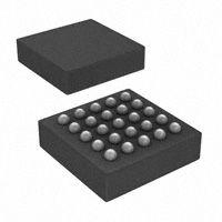
µTFBGA25
.
The STCCP27A receiver converts the subLVDS
clock/datastream (up to 416 Mbps throughput
bandwidth) back into parallel 8 bits of CMOS/
LVTTL. The device recognizes the CCP 32bit
start of frame (SOF), end of frame (EOF), start of
line (SOL) and end of line (EOL) sequences to
generate the H-SYNC and V-SYNC signals.
Output LVTTL clock (up to 52 MHz) is transmitted
in parallel with data. Input and Output data are
rising edge strobe. This chipset is an ideal means
to link mobile camera modules to baseband
processors. In order to minimize static current
consumption, it is possible to shut down the
device when the interface is not being used by a
power-down (EN) pin that reduces to 10µA the
Maximum Current Consumption making this
device ideal for portable applications like Mobile
Phone, Portable Battery Equipment. Two
dedicated I2C lines are provided to translate
bidirectional controls from camera and µC
devices. The STCCP27A is offered in a µTFBGA
package to optimize PCB space. All inputs and
outputs are equipped with protection circuits
against static discharge, giving them ESD
immunity from transient excess voltage. The
STCCP27A is characterized for operation over
the commercial temperature range -40°C to 85°C.
Order code
Part number
Temperature
Range
Package
Comments
STCCP27ATBR
-40 to 85 °C
µTFBGA25 3x3mm (Tape & Reel)
3000 parts per reel
April 2006
Rev. 1
1/19
www.st.com
19
�STCCP27A
Contents
1
Schematic diagram
......................................... 3
2
Pin configuration . . . . . . . . . . . . . . . . . . . . . . . . . . . . . . . . . . . . . . . . . . . 5
3
Maximum ratings . . . . . . . . . . . . . . . . . . . . . . . . . . . . . . . . . . . . . . . . . . . . 7
4
Electrical characteristics . . . . . . . . . . . . . . . . . . . . . . . . . . . . . . . . . . . . . 8
)
s
(
t
c
u
d
o
)
r
s
(
P
t
c
e
t
u
e
d
l
o
o
r
s
P
b
e
O
t
e
l
)
o
s
(
s
t
b
c
u
O
d
o
)
r
s
P
(
t
c
e
t
u
e
l
d
o
o
r
s
P
b
O
e
t
e
l
o
s
b
O
5
Timing diagram . . . . . . . . . . . . . . . . . . . . . . . . . . . . . . . . . . . . . . . . . . . . 10
6
Package mechanical data . . . . . . . . . . . . . . . . . . . . . . . . . . . . . . . . . . . . 15
7
Revision history . . . . . . . . . . . . . . . . . . . . . . . . . . . . . . . . . . . . . . . . . . . 18
2/19
�STCCP27A
Schematic diagram
1
Schematic diagram
Figure 1.
Simplified application block diagram
)
s
(
t
c
u
d
o
)
r
s
(
P
t
c
e
t
u
e
d
l
o
o
r
s
P
b
e
O
t
e
l
)
o
s
(
s
t
b
c
u
O
d
o
)
r
s
P
(
t
c
e
t
u
e
l
d
o
o
r
s
P
b
O
e
t
e
l
o
s
b
O
Figure 2.
Block diagram
3/19
�Schematic diagram
Figure 3.
STCCP27A
Simplified I2C line block diagram
)
s
(
t
c
u
d
o
)
r
s
(
P
t
c
e
t
u
e
d
l
o
o
r
s
P
b
e
O
t
e
l
)
o
s
(
s
t
b
c
u
O
d
o
)
r
s
P
(
t
c
e
t
u
e
l
d
o
o
r
s
P
b
O
e
t
e
l
o
s
b
O
4/19
�STCCP27A
Pin configuration
2
Pin configuration
Figure 4.
Pin configuration (top through view - bumps are on the other side)
)
s
(
t
c
u
d
o
)
r
s
(
P
t
c
e
t
u
e
d
l
o
o
r
s
P
b
e
O
t
e
l
)
o
s
(
s
t
b
c
u
O
d
o
)
r
s
P
(
t
c
e
t
u
e
l
d
o
o
r
s
P
b
O
e
t
e
l
o
s
b
O
Table 1.
Pin description
Pin n°
Symbol
D5
E5
D4
E4
D2
E2
D1
E1
A2, A1
A5, A4
B3
D3
C3
B2
A3, E3
C5
B4
C1
B1, C2
B5, C4
D1
D2
D3
D4
D5
D6
D7
D8
D+, DCLK+, CLKEN
CLK
H-SYNC
V-SYNC
GND
VDD
SYNC SEL
VL
I/OVL1, I/OVL2
I/OVDD1, I/OVDD2
Name and function
Decoder Output (LSB)
Decoder Output
Decoder Output
Decoder Output
Decoder Output
Decoder Output
Decoder Output
Decoder Output (MSB)
Differential Data Receiver Inputs
Differential CLK Receiver Inputs
Receivers Enable Input
Clock Output
Horizontal Sync Output
Vertical Sync Output
Ground
Main Supply Voltage
Select Sync Input
Secondary Supply Voltage
I2C Line (VL Referred)
I2C Line (VDD Referred)
5/19
�Pin configuration
STCCP27A
Table 2.
Main function table
Input
Enable SYNC_SEL
L
H
H
H
H
X
H
H
H
H
H
L
D+
Output
D-
CLK+ CLK-
X
X
X
X
SOF (FFH 00H 00H 02H)
EOF(FFH 00H 00H 03H)
SOL(FFH 00H 00H 00H)
EOL(FFH 00H 00H 01H)
X
X
X
V-SYNC
H-SYNC
D1-D8
CLK
L
H
L
No change
No change
L
H
L
H
L
L
L
L
L
X
Function
CCP disabled
Start of frame
End of frame
See detailed
timing diagram
Start of line
End of line
See
Disabled sync
detailed (D1-D8 will get out
D+, Dtiming
data, including
diagram
sync code)
)
s
(
t
c
u
d
o
)
r
s
(
P
t
c
e
t
u
e
d
l
o
o
r
s
P
b
e
O
t
e
l
)
o
s
(
s
t
b
c
u
O
d
o
)
r
s
P
(
t
c
e
t
u
e
l
d
o
o
r
s
P
b
O
e
t
e
l
o
s
b
O
Z = High Impedance, L = Low Voltage Level, H = High Voltage Level, X = Don’t care
Table 3.
Enable
X
X
X
X
I2C
Bus function table
I/O Input
I/OVDD
I/OVL
L
VDD
Open
VDD
L
VL
VL
Open
Function
I2C Comm.
I2C Comm.
I2C Comm.
I2C Comm.
Open: If I/OVDD is not driven then the I/OVL will go in high level VL by embedded 10kΩ pull-up resistor; If I/OVL
is not driven then the I/OVCC will go in high level VDD by embedded 10KΩ pull-up resistor
Figure 5.
6/19
Frame structure In VGA case (allowed synchronization codes sequence)
�STCCP27A
3
Maximum ratings
Maximum ratings
Table 4.
Symbol
VDD
VL
VD
VCLK
VI
VO
VI/OVL
TSTG
Absolute maximum ratings
Parameter
Main supply voltage
Secondary supply voltage
SubLVDS data bus input voltage (D+, D-)
SubLVDS clock bus input voltage (CLK+, CLK-)
DC input voltage (SYNC_SEL, EN)
DC output voltage (D1-D8, H-SYNC, V-SYNC, CLK, I/OVDD)
DC output voltage (I/OVL)
Storage temperature range
Electrostatic discharge protection
HBM Human body model (all pins)
Value
Unit
-0.5 to 4.6
-0.5 to 4.6
-0.5 to 4.6
-0.5 to 4.6
-0.5 to 4.6
-0.5 to (VDD + 0.5)
-0.5 to (VL + 0.5)
-65 to +150
V
V
V
V
V
V
V
°C
±2
kV
)
s
(
t
c
u
d
o
)
r
s
(
P
t
c
e
t
u
e
d
l
o
o
r
s
P
b
e
O
t
e
l
)
o
s
(
s
t
b
c
u
O
d
o
)
r
s
P
(
t
c
e
t
u
e
l
d
o
o
r
s
P
b
O
e
t
e
l
o
s
b
O
ESD
Note:
Absolute Maximum Ratings are those values beyond which damage to the device may
occur. Functional operation under these condition is not implied.
Table 5.
Symbol
Recommended operating conditions
Parameter
Main supply voltage
Secondary supply voltage
Differential level input voltage (D+, D-, CLK1+, CLK1-)
Common level input voltage (D+, D-, CLK1+, CLK1-)
Level input voltage (SYNC_SEL, EN)
VI/OVDD Level input voltage (I/OVDD)
VI/OVL Level input voltage (I/OVL)
RT
Termination resistance (per pair differential input line)
CL
Termination capacitance (per line vs gnd pin)
TA
Operating ambient temperature range
TJ
Operating junction temperature range
tR, tF Rise and fall time (I/OVDD, I/OVL; 10% to 90%; 90% to 10%)
VDD
VL
VID
VCM
VIC
Min.
Typ.
Max.
Unit
2.65
1.65
0.1
0.5
2.8
1.8
80
100
10
3.6
1.95
0.4
1.3
3.6
VDD
VL
120
V
V
V
V
V
V
V
Ω
pF
°C
°C
ns
-40
-40
0.9
85
125
600
7/19
�Electrical characteristics
4
STCCP27A
Electrical characteristics
Table 6.
Symbol
VCM
II
Electrical characteristics (Over recommended operating conditions unless
otherwise noted. All typical values are at TA = 25°C, and VDD = 2.8V, VL = 1.8V)
Parameter
Common mode input
voltage (see fig.1)
Input leakage current
(D+, D-, CLK1+, CLK1-)
Test conditions
RT = 100Ω ± 1%
VI = 0.4V
VI = 1.4V
EN=VDD,
I/OVL = VL, I/OVDD = VDD,
D+, CLK+ = Gnd or VDD,
D+, CLK+ = VDD or Gnd
EN=Gnd, VDD=2.65V to 3.6V
VL=1.65V to 1.95V
VDD = 2.65V to 3.6V
VL = 1.65V to 1.95V
VDD = 2.65V to 3.6V
VL = 1.65V to 1.95V
Min.
Typ.
Max.
Unit
0.5
0.9
1.3
V
±10
±10
µA
µA
)
s
(
t
c
u
d
o
)
r
s
(
P
t
c
e
t
u
e
d
l
o
o
r
s
P
b
e
O
t
e
l
)
o
s
(
s
t
b
c
u
O
d
o
)
r
s
P
(
t
c
e
t
u
e
l
d
o
o
r
s
P
b
O
e
t
e
l
o
s
b
O
IS
ISOFF
VIH
VIL
IIH
IIL
VOH
VOL
VIH2
VIL2
VOH2
VOL2
8/19
Supply current (IL + IDD)
Shutdown supply current
(IL+ IDD)
HIGH Level input voltage
(SYNC_SEL, EN)
LOW Level input voltage
(SYNC_SEL, EN)
HIGH Level input current
(SYNC_SEL, EN)
LOW Level input current
(SYNC_SEL, EN)
HIGH Level output voltage
(D1-D8, H-SYNC, V-SYNC,
CLK)
LOW Level output voltage
(D1-D8, H-SYNC, V-SYNC,
CLK)
HIGH Level input voltage
(I/OVL1, I/OVL2)
HIGH Level input voltage
(I/OVDD1, I/OVDD2)
LOW Level input voltage
(I/OVL1, I/OVL2)
LOW Level input voltage
(I/OVDD1, I/OVDD2)
HIGH Level output voltage
(I/OVL1, I/OVL2)
HIGH Level output voltage
(I/OVDD1, I/OVDD2)
LOW Level output voltage
(I/OVL1, I/OVL2, I/OVDD1,
I/OVDD2)
3.6
7.0
mA
10
µA
0.7xVDD
3.6
V
0
0.3xVDD
V
VIH = 0.7xVDD
±10
µA
VIL= 0.3xVDD
±10
µA
IOH = -8mA
2.0
V
IOH = -4mA
2.4
V
IOL = +8mA
VDD = 2.65V to 3.6V
VL = 1.65V to 1.95V
VDD = 2.65V to 3.6V
VL = 1.65V to 1.95V
VDD = 2.65V to 3.6V
VL = 1.65V to 1.95V
VDD = 2.65V to 3.6V
VL = 1.65V to 1.95V
IOH = -20µA
VI/OVDD = VDD
IOH = -20µA
VI/OVL = VL
IOL= +1mA,
VI/OVLor VI/OVDD = Gnd
0.60
V
0.7xVL
V
0.7xVDD
V
0
0.25
V
0
0.25
V
VL-0.4
V
VDD-0.4
V
0.35
V
�STCCP27A
Electrical characteristics
Table 7.
Symbol
Switching characteristics (RT = 100Ω ± 1%, CL = 10pF, over recommended
operating conditions unless otherwise noted. Typical values are referred to TA =
25°C and VDD = 2.8V, VL = 1.8V)
Parameter
Test conditions
Rise time LVTTL Output voltage
(10% to 90%)
Fall time LVTTL output voltage
(90% to 10%)
Rise time I2C input/output voltage
(20% to 80%)
Fall time I2C input/output voltage
(80% to 20%)
Propagation delay time (CLK to VSYNC, H-SYNC) (low to high)
Propagation delay time (CLK to VSYNC, H-SYNC) (high to low)
Propagation delay time (CLK to
D1-D8) (low to high)
Propagation delay time (CLK to
D1-D8) (high to low)
Propagation delay time I2C
input/output voltage (50% to 50%)
(Low to High)
Propagation delay time I2C
input/output voltage (50% to 50%)
(High to Low)
Enable delay time (EN to
V-SYNC, H-SYNC: tPZL, tPZH)
Disable delay time (EN to VSYNC, H-SYNC: tPLZ, tPHZ)
tr
tf
tr I/O
tf I/O
tpLH
tpHL
tpLH
tpHL
tpLH
tpHL
tEN
u
d
o
Operating frequency
fOPR
TCLK
r
P
e
s
b
O
s
b
O
1
Symbol
CIN
Unit
3.1
4.0
ns
2.0
4.0
ns
320
ns
20
ns
o
s
b
O
)
e
t
le
trEN = 2.0ns (10% to 90%)
tfEN = 2.0ns (90% to 10%)
trEN = 2.0ns (10% to 90%)
tfEN = 2.0ns (90% to 10%)
trD,CLK = 400ps (10% to 90%)
tfD,CLK = 400ps (90% to 10%)
VCM D,CLK = 0.9V, VDD,CLK =
150mV
o
s
b
O
-
)
s
(
ct
u
d
o
ns
6.5
t
c
u
8.5
ns
6.5
8.5
ns
100
ns
10
ns
20
µs
1000
ns
1
416
MHz
2.4
1000
ns
Pr
e
t
e
l
8.5
(s)
8.5
od
r
P
e
t
e
l
o
Note:
Max.
6.5
Clock Period
Setup time (D to CLK) (low to high
tSUD-CLK or high to low vs positive CLK
edge) (note 1) (see fig. 6)
Hold time (CLK to D) (positive CLK
tHCLK-D
edge to D) (note 1) (see fig. 6)
t
e
l
o
Typ.
6.5
s
(
t
c
tDIS
Min.
c
u
d
o
r
P
ns
)
s
t(
0.6
ns
1.0
ns
50% VDIN to 50% VDOUT
Table 8.
Capacitive characteristics
Test condition
Parameter
Input Capacitance
(SYNC_SEL, EN)
TA = 25°C
VDD (V)
2.65 to 3.6
Value
Min.
VL = 1.65V to 1.95V,
VI = GND or VDD
Typ.
3.5
Unit
Max.
pF
9/19
�Timing diagram
5
STCCP27A
Timing diagram
(unless otherwise specified TA = 25°C)
Figure 6.
tSUD-CLK , tHCLK-D (Differential input signals D+,D- and CLK+,CLK-)
)
s
(
t
c
u
d
o
)
r
s
(
P
t
c
e
t
u
e
d
l
o
o
r
s
P
b
e
O
t
e
l
)
o
s
(
s
t
b
c
u
O
d
o
)
r
s
P
(
t
c
e
t
u
e
l
d
o
o
r
s
P
b
O
e
t
e
l
o
s
b
O
Figure 7.
Bit order in synchronization codes and data, LSB first (example start of frame), image
frame structure
Note:
LSB (bytewise Least Significant Bit first)
10/19
�STCCP27A
Figure 8.
Timing diagram
Disabled sync mode free running clock IN (SYNC_SEL=GND) (D1-D8 will get out input
data DIN, including sync code)
)
s
(
t
c
u
d
o
)
r
s
(
P
t
c
e
t
u
e
d
l
o
o
r
s
P
b
e
O
t
e
l
)
o
s
(
s
t
b
c
u
O
d
o
)
r
s
P
(
t
c
e
t
u
e
l
d
o
o
r
s
P
b
O
e
t
e
l
o
s
b
O
11/19
�Timing diagram
Figure 9.
STCCP27A
Enabled sync mode free running clock IN (SYNC_SEL=VDD) (D1-D8 will get out input
data DIN only, excluding sync code)
)
s
(
t
c
u
d
o
)
r
s
(
P
t
c
e
t
u
e
d
l
o
o
r
s
P
b
e
O
t
e
l
)
o
s
(
s
t
b
c
u
O
d
o
)
r
s
P
(
t
c
e
t
u
e
l
d
o
o
r
s
P
b
O
e
t
e
l
o
s
b
O
12/19
�STCCP27A
Timing diagram
Figure 10. Enabled sync mode gated clock IN (SYNC_SEL=VDD) (D1-D8 will get out input data
DIN only, excluding sync code)
)
s
(
t
c
u
d
o
)
r
s
(
P
t
c
e
t
u
e
d
l
o
o
r
s
P
b
e
O
t
e
l
)
o
s
(
s
t
b
c
u
O
d
o
)
r
s
P
(
t
c
e
t
u
e
l
d
o
o
r
s
P
b
O
e
t
e
l
o
s
b
O
13/19
�Timing diagram
STCCP27A
Figure 11. Enabled sync mode free running clock IN (SYNC_SEL=VDD) (D1-D8 will get out input
data DIN only, excluding sync code
)
s
(
t
c
u
d
o
)
r
s
(
P
t
c
e
t
u
e
d
l
o
o
r
s
P
b
e
O
t
e
l
)
o
s
(
s
t
b
c
u
O
d
o
)
r
s
P
(
t
c
e
t
u
e
l
d
o
o
r
s
P
b
O
e
t
e
l
o
s
b
O
Figure 12. Disabled sync mode free running clock IN (SYNC_SEL=Gnd) (D1-D8 will get out input
data DIN only, excluding sync code)
14/19
�STCCP27A
6
Package mechanical data
Package mechanical data
In order to meet environmental requirements, ST offers these devices in ECOPACK®
packages. These packages have a Lead-free second level interconnect. The category of
second Level Interconnect is marked on the package and on the inner box label, in
compliance with JEDEC Standard JESD97. The maximum ratings related to soldering
conditions are also marked on the inner box label. ECOPACK is an ST trademark.
ECOPACK specifications are available at: www.st.com.
)
s
(
t
c
u
d
o
)
r
s
(
P
t
c
e
t
u
e
d
l
o
o
r
s
P
b
e
O
t
e
l
)
o
s
(
s
t
b
c
u
O
d
o
)
r
s
P
(
t
c
e
t
u
e
l
d
o
o
r
s
P
b
O
e
t
e
l
o
s
b
O
15/19
�Package mechanical data
STCCP27A
µTFBGA25 MECHANICAL DATA
mm.
mils
DIM.
A
MIN.
TYP
MAX.
MIN.
TYP.
MAX.
1.0
1.1
1.16
39.4
43.3
45.7
A1
0.25
A2
0.78
b
0.25
D
2.9
9.8
0.86
30.7
33.9
0.30
0.35
9.8
11.8
13.8
3.0
3.1
114.2
118.1
122.0
)
s
(
t
c
u
d
o
)
r
s
(
P
t
c
e
t
u
e
d
l
o
o
r
s
P
b
e
O
t
e
l
)
o
s
(
s
t
b
c
u
O
d
o
)
r
s
P
(
t
c
e
t
u
e
l
d
o
o
r
s
P
b
O
e
t
e
l
o
s
b
O
D1
E
2
2.9
3.0
78.8
3.1
114.2
118.1
E1
2
78.8
e
0.5
19.7
SE
0.25
9.8
122.0
7539979/A
16/19
�STCCP27A
Package mechanical data
Tape & Reel TFBGA25 MECHANICAL DATA
mm.
inch
DIM.
MIN.
TYP
A
MAX.
MIN.
TYP.
330
13.2
MAX.
12.992
C
12.8
0.504
D
20.2
0.795
N
60
2.362
0.519
)
s
(
t
c
u
d
o
)
r
s
(
P
t
c
e
t
u
e
d
l
o
o
r
s
P
b
e
O
t
e
l
)
o
s
(
s
t
b
c
u
O
d
o
)
r
s
P
(
t
c
e
t
u
e
l
d
o
o
r
s
P
b
O
e
t
e
l
o
s
b
O
T
14.4
0.567
Ao
3.3
0.130
Bo
3.3
0.130
Ko
1.60
0.063
Po
3.9
4.1
0.153
0.161
P
7.9
8.1
0.311
0.319
17/19
�Revision history
STCCP27A
7
Revision history
Table 9.
Revision history
Date
Revision
12-Apr-2006
1
Changes
Initial release.
)
s
(
t
c
u
d
o
)
r
s
(
P
t
c
e
t
u
e
d
l
o
o
r
s
P
b
e
O
t
e
l
)
o
s
(
s
t
b
c
u
O
d
o
)
r
s
P
(
t
c
e
t
u
e
l
d
o
o
r
s
P
b
O
e
t
e
l
o
s
b
O
18/19
�STCCP27A
)
s
(
t
c
u
d
o
)
r
s
(
P
t
c
e
t
u
e
d
l
o
o
r
s
P
b
e
O
t
e
l
)
o
s
(
s
t
b
c
u
O
d
o
)
r
s
P
(
t
c
e
t
u
e
l
d
o
o
r
s
P
b
O
e
t
e
l
o
s
b
O
Please Read Carefully:
Information in this document is provided solely in connection with ST products. STMicroelectronics NV and its subsidiaries (“ST”) reserve the
right to make changes, corrections, modifications or improvements, to this document, and the products and services described herein at any
time, without notice.
All ST products are sold pursuant to ST’s terms and conditions of sale.
Purchasers are solely responsible for the choice, selection and use of the ST products and services described herein, and ST assumes no
liability whatsoever relating to the choice, selection or use of the ST products and services described herein.
No license, express or implied, by estoppel or otherwise, to any intellectual property rights is granted under this document. If any part of this
document refers to any third party products or services it shall not be deemed a license grant by ST for the use of such third party products
or services, or any intellectual property contained therein or considered as a warranty covering the use in any manner whatsoever of such
third party products or services or any intellectual property contained therein.
UNLESS OTHERWISE SET FORTH IN ST’S TERMS AND CONDITIONS OF SALE ST DISCLAIMS ANY EXPRESS OR IMPLIED
WARRANTY WITH RESPECT TO THE USE AND/OR SALE OF ST PRODUCTS INCLUDING WITHOUT LIMITATION IMPLIED
WARRANTIES OF MERCHANTABILITY, FITNESS FOR A PARTICULAR PURPOSE (AND THEIR EQUIVALENTS UNDER THE LAWS
OF ANY JURISDICTION), OR INFRINGEMENT OF ANY PATENT, COPYRIGHT OR OTHER INTELLECTUAL PROPERTY RIGHT.
UNLESS EXPRESSLY APPROVED IN WRITING BY AN AUTHORIZE REPRESENTATIVE OF ST, ST PRODUCTS ARE NOT DESIGNED,
AUTHORIZED OR WARRANTED FOR USE IN MILITARY, AIR CRAFT, SPACE, LIFE SAVING, OR LIFE SUSTAINING APPLICATIONS,
NOR IN PRODUCTS OR SYSTEMS, WHERE FAILURE OR MALFUNCTION MAY RESULT IN PERSONAL INJURY, DEATH, OR
SEVERE PROPERTY OR ENVIRONMENTAL DAMAGE.
Resale of ST products with provisions different from the statements and/or technical features set forth in this document shall immediately void
any warranty granted by ST for the ST product or service described herein and shall not create or extend in any manner whatsoever, any
liability of ST.
ST and the ST logo are trademarks or registered trademarks of ST in various countries.
Information in this document supersedes and replaces all information previously supplied.
The ST logo is a registered trademark of STMicroelectronics. All other names are the property of their respective owners.
© 2006 STMicroelectronics - All rights reserved
STMicroelectronics group of companies
Australia - Belgium - Brazil - Canada - China - Czech Republic - Finland - France - Germany - Hong Kong - India - Israel - Italy - Japan Malaysia - Malta - Morocco - Singapore - Spain - Sweden - Switzerland - United Kingdom - United States of America
www.st.com
19/19
�


 工商网监
湘ICP备2023018690号
工商网监
湘ICP备2023018690号
