STCF01
Step-up converter for cell phone camera flash LEDs
General features
■
Supply voltage range: 2.6V to 5.5V
■
17V Maximum output voltage
■
Two current levels up to 300mA set with
external resistors
■
Dedicated pin to select the required level of
current
■
Operating frequency: 1.5MHz: PWM Controller
■
Torch mode supported
■
Shutdown pin with true load disconnection
■
Efficiency: 90% at 100mA; 80% at 300mA
■
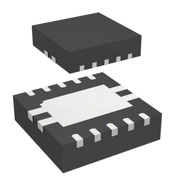
DFN10L (3mm x 3mm) Package
)
s
(
t
c
u
d
o
)
r
s
(
P
t
c
e
t
u
e
d
l
o
o
r
s
Description
P
b
e
O
t
e
l
)
o
s
(
s
t
b
c
u
O
d
o
)
r
s
P
(
t
c
e
t
u
e
l
d
o
o
r
s
P
b
O
e
t
e
l
o
s
b
O
DFN10L (3x3)
to set the required current for each level.
Compared to the linear current control technique,
this method allows designers to achieve the best
and most efficient performance possible with the
selected current, thereby avoiding linear element
losses.
The STCF01 is a dedicated IC designed to drive
two, three, or four white, cell phone camera flash
LEDs with constant current. The step-up (boost)
converter input is connected directly to the battery,
and its converter output voltage is automatically
determined using current feedback-based duty
cycle control.
The STCF01 has a dedicated pin for two levels of
LED current selection. An external resistor is used
The Shutdown (SHDN) pin saves power when the
camera flash is not used by consuming less than
0.1µA of current. When the SHDN pin is high
(logic '1'), the device is turned OFF and there is no
DC current path from the supply to the white LEDs
(Load Disconnect). If it is held to GND, the output
current continuously flows through the LEDs
(Torch mode). The SHDN pin, when it is set to low
(logic '0'), is also used to set the flash function
time duration.
Order code
Part number
Package
Packaging
STCF01PMR
DFN10L (3mm x 3mm)
4500 parts per reel
October 2006
Rev. 4
1/16
www.st.com
16
�STCF01
Contents
Contents
1
Diagram . . . . . . . . . . . . . . . . . . . . . . . . . . . . . . . . . . . . . . . . . . . . . . . . . . . . . 3
2
Pin configuration . . . . . . . . . . . . . . . . . . . . . . . . . . . . . . . . . . . . . . . . . . . . . 4
3
Application information . . . . . . . . . . . . . . . . . . . . . . . . . . . . . . . . . . . . . . . . 5
4
Maximum ratings . . . . . . . . . . . . . . . . . . . . . . . . . . . . . . . . . . . . . . . . . . . . . . 6
5
Electrical characteristics . . . . . . . . . . . . . . . . . . . . . . . . . . . . . . . . . . . . . . . 7
6
Detailed description . . . . . . . . . . . . . . . . . . . . . . . . . . . . . . . . . . . . . . . . . . . 8
7
Typical operating characteristics . . . . . . . . . . . . . . . . . . . . . . . . . . . . . . . . . 9
8
Package mechanical data . . . . . . . . . . . . . . . . . . . . . . . . . . . . . . . . . . . . . . 12
9
Revision history . . . . . . . . . . . . . . . . . . . . . . . . . . . . . . . . . . . . . . . . . . . . . 15
)
s
(
t
c
u
d
o
)
r
s
(
P
t
c
e
t
u
e
d
l
o
o
r
s
P
b
e
O
t
e
l
)
o
s
(
s
t
b
c
u
O
d
o
)
r
s
P
(
t
c
e
t
u
e
l
d
o
o
r
s
P
b
O
e
t
e
l
o
s
b
O
2/16
�STCF01
1
Figure 1.
Diagram
Diagram
Block diagram
)
s
(
t
c
u
d
o
)
r
s
(
P
t
c
e
t
u
e
d
l
o
o
r
s
P
b
e
O
t
e
l
)
o
s
(
s
t
b
c
u
O
d
o
)
r
s
P
(
t
c
e
t
u
e
l
d
o
o
r
s
P
b
O
e
t
e
l
o
s
b
O
3/16
�STCF01
Pin configuration
2
Pin configuration
Figure 2.
Pin connections (top view)
)
s
(
t
c
u
d
o
)
r
s
(
P
t
c
e
t
u
e
d
l
o
o
r
s
P
b
e
O
t
e
l
)
o
s
(
s
t
b
c
u
O
d
o
)
r
s
P
(
t
c
e
t
u
e
l
d
o
o
r
s
P
b
O
e
t
e
l
o
s
b
O
Table 1.
Pin description
Pln N°
Symbol
1
PWRGND
2
OVP
3
VI
4
HC
5
LC
6
SGLGND
7
FB
8
SEL
9
SHDN
10
SW
4/16
Note
This is the application power signal reference. Connect the input and output capacitors to
this pin.
This pin senses step-up output voltage, which provides overvoltage protection in the event
that the output voltage exceeds the OVP threshold
This pin supplies the input voltage for the step-up stage as well as the supply voltage for the
overall device.
This pin sets the high level current for the white LEDs with a resistor that is connected
between this pin and VI.
This pin sets the low level current for the white LEDs with a resistor that is connected
between this pin and VI.
This pin is the logic signal reference for the IC.
This pin senses the current flowing through the white LEDs and uses this feedback to
provide current regulation.
This pin is used to select the signal level of the white LEDs; a low level signal sets the low
level LED current, while the high level signal sets the high level LED current.
This pin enables or disables the Shutdown mode. A high level signal enables device
Shutdown mode, where most of the device internal logic is turned OFF. If this pin is held to
GND, the output current flows through the LEDs continuously (Torch mode).
This is the switch node pin, which is connected to the internal N-channel MOSFET drain.
�STCF01
3
Figure 3.
Application information
Application information
Application circuit
)
s
(
t
c
u
d
o
)
r
s
(
P
t
c
e
t
u
e
d
l
o
o
r
s
P
b
e
O
t
e
l
)
o
s
(
s
t
b
c
u
O
d
o
)
r
s
P
(
t
c
e
t
u
e
l
d
o
o
r
s
P
b
O
e
t
e
l
o
s
b
O
5/16
�STCF01
Maximum ratings
4
Maximum ratings
Table 2.
Absolute maximum ratings
Symbol
Parameter
VI
VSW
FB, SEL,
SHDN, LC, HC
OVP
ESD
PTOT
Value
Unit
DC Input Voltage to SGLGND
-0.3 to 6
V
Switch Voltage
-0.3 to 20
V
Voltage Range
-0.3 to VI + 0.3
V
Over Voltage Protection
Human Body Model
Continuous Power Dissipation (at TA = 70°C)
-0.3 to 20
±2
500
V
kV
mW
Operating Junction Temperature Range
-40 to 85
°C
Junction Temperature
-40 to 125
°C
Storage Temperature Range
-65 to 150
°C
)
s
(
t
c
u
d
o
)
r
s
(
P
t
c
e
t
u
e
d
l
o
o
r
s
P
b
e
O
t
e
l
)
o
s
(
s
t
b
c
u
O
d
o
)
r
s
P
(
t
c
e
t
u
e
l
d
o
o
r
s
P
b
O
e
t
e
l
o
s
b
O
TOP
TJ
TSTG
Note:
Table 3.
Symbol
Absolute Maximum Ratings are those values beyond which damage to the device may occur.
Functional Operation under these conditions is not implied.
Thermal data
Parameter
Value
Unit
RthJA
Thermal Resistance Junction-Ambient
30.9
°C/W
RthJC
Thermal Resistance Junction-Case
2.96
°C/W
6/16
�STCF01
5
Electrical characteristics
Electrical characteristics
Table 4.
DC Electrical characteristics
(TJ = -40°C to 85°C, VI = 3.6V, CI = 2.2µF, CO = 4.7µF, L = 10µH, RLC = 12kΩ, RHC = 4kΩ,
VOVP = 8V, Typ. values @ 25°C, unless otherwise specified)
Symbol
Parameter
Test Conditions
Min.
Typ.
Max.
Unit
5.5
V
General section
VI
Max Operation Supply Voltage
VUVLO
IQ
Under Voltage lockout threshold
Quiescent Current
fSW
VSEL= 0V, VSHDN = 0V,
Min. duty cycle
VSEL= 0V
Shutdown Mode
VSEL= 0V, VSHDN = 0V
Switching Frequency
VOVP
Over Voltage Threshold
IPKMax
Maximum Inductor Current
No Load
VSHDN = 0V
VHC
HC Pin Voltage
VSEL= 3V, VSHDN = 0V
VLC
LC Pin Voltage
VSEL= 0V, VSHDN = 0V
ILED/IHC
High Level Current Multiplier
ILED/ILC
Low Level Current Multiplier
Resistance ON Feedback
IFB = 100mA
IFB(LEAK)
e
t
e
l
RON
DMIN
e
t
e
ol
u
d
o
Control input section
s
b
O
r
P
e
VH(SEL) SEL and SHDN Input High
VH(SHDN) Threshold
t
e
l
o
VL(SEL)
VL(SHDN)
bs
SEL and SHDN Input Low
Threshold
V
c
u
d
)
s
t(
A
V
VI-0.55
V
VSEL= 3V, VSHDN = 0V (25°C)
1900
2100
2300
A/A
VSEL= 0V, VSHDN = 0V (25°C)
2200
2400
2600
A/A
1
µA
b
O
e
t
le
o
r
P
(s)
Ω
1.2
o
s
b
O
-
0.1
ISW = 1A Note: 1
ct
Minimum Duty Cycle
1.2
19
VI-0.55
Ω
0.3
ISW(LEAK) Internal Switch Leakage Current VSHDN = 3V, VSW= 16.5V
DMAX
IFB = 0mA
Maximum Duty Cycle
o
r
P
18
mA
µA
MHz
VI-0.6
)-
du
Pr
3
0.5
1.8
VI-0.65
VSHDN = 3V, VFB = VI
Internal Switch ON-Resistance
u
d
o
ct
V
VI-0.6
s
(
t
c
Switch section
1.2
2.3
0.1
1.5
(s)
2.6
VI-0.65
so
Current Feedback Leakage
2.45
17
Current control
RONFB
2.3
0.1
IFB = 200mA; VSEL = 0V
Pulse Skipping
VI = 2.6V
1.2
VI = 3.6V
1.4
VI = 5.5V
1.6
1
µA
90
%
0
%
V
VI = 2.6V
0.4
VI = 3.6V
0.5
VI = 5.5V
0.6
V
Thermal shutdown
O
TSD
Thermal Shutdown
145
°C
THS
Thermal Shutdown Hysteresis
15
°C
Note: 1 Typical value, not production tested
7/16
�Detailed description
6
STCF01
Detailed description
The STCF01 white Led boost converter drives from two up to four white LEDs with a constant
current. It needs few external components: two ceramic capacitors (CI=2.2µF CO=4.7µF), one
inductor L=10µH and one schottky diode. The device works with a minimum VI=2.6V, and it has
an Over Voltage Protection on the output guaranteed at minimum value equal to 17V. This
value ensures proper operation with a maximum of four White LEDs in series. In the worst case
of VI=2.6V at VOVP=8V (typical value of two LEDs) it is possible to obtain IO=270mA, while at
VOVP=11V (typical value of three LEDs) it is possible obtain IO=180mA (Figure 4). The
maximum IO current is limited by inductor peak current internally set at Typ 1.2A. This feature
allows for a longer battery life as it reduces intensive use of the flash. The SEL pin allows
selection of high and low current values flowing on the White LEDs.
)
s
(
t
c
u
d
o
)
r
s
(
P
t
c
e
t
u
e
d
l
o
o
r
s
P
b
e
O
t
e
l
)
o
s
(
s
t
b
c
u
O
d
o
)
r
s
P
(
t
c
e
t
u
e
l
d
o
o
r
s
P
b
O
e
t
e
l
o
s
b
O
The two current values are set through external resistors RHC and RLC according to the
following formula:
ILED(FLASH) = 2100 * (VI - VHC) / RHC
ILED(TORCH) = 2400 * (VI - VLC) / RLC
A High logic level on SHDN pin puts the device in shutdown mode; if it is held at LOW the flash
or torch mode is activated. When the SHDN pin is LOW the device provides the requested
current in less than 200µs (see TURN ON TIME plot). This fast turn-on time makes the device
suitable for single shoot and multiple shoot operation modes.
8/16
�STCF01
7
Typical operating characteristics
Typical operating characteristics
(TJ = -40°C to 85°C, VI = 3.6V, CI = 2.2µF, CO = 4.7µF, L = 10µH, RLC = 12kΩ, RHC = 4kΩ, VOVP
= 8V, Typ. values @ 25°C, unless otherwise specified).
Figure 4. Maximum output current vs input
Figure 5. Maximum output current vs input
voltage
voltage
)
s
(
t
c
u
d
o
)
r
s
(
P
t
c
e
t
u
e
d
l
o
o
r
s
P
b
e
O
t
e
l
)
o
s
(
s
t
b
c
u
O
d
o
)
r
s
P
(
t
c
e
t
u
e
l
d
o
o
r
s
P
b
O
e
t
e
l
o
s
b
O
Figure 6.
Efficiency vs temperature
Figure 7.
Efficiency vs temperature
Figure 8.
Efficiency vs temperature
Figure 9.
Quiescent current at full operation
vs. temperature
9/16
�STCF01
Typical operating characteristics
.
Figure 10. Feedback voltage vs temperature
Figure 11. Current feedback leakage vs
temperature
)
s
(
t
c
u
d
o
)
r
s
(
P
t
c
e
t
u
e
d
l
o
o
r
s
P
b
e
O
t
e
l
)
o
s
(
s
t
b
c
u
O
d
o
)
r
s
P
(
t
c
e
t
u
e
l
d
o
o
r
s
P
b
O
e
t
e
l
o
s
b
O
Figure 12. VI-VLC vs temperature
Figure 13. VI-VHC vs temperature
Figure 14. Peak inductor current vs
temperature
Figure 15. RONFB vs temperature
10/16
�STCF01
Typical operating characteristics
.
Figure 16. Maximum duty cycle vs temperature Figure 17. Turn on and off response
)
s
(
t
c
u
d
o
)
r
s
(
P
t
c
e
t
u
e
d
l
o
o
r
s
P
b
e
O
t
e
l
)
o
s
(
s
t
b
c
u
O
d
o
)
r
s
P
(
t
c
e
t
u
e
l
d
o
o
r
s
P
b
O
e
t
e
l
o
s
b
O
VSHDN=pulse, FREQ.=1Hz, Tr=Tf=10µs
Figure 18. Turn on time
Figure 19. Start up transient
VSHDN=pulse, FREQ.=1Hz, Tr=Tf=10µs
VI=0 to 3.6V, VSEL=GND, VSHDN=GND
Figure 20. Multi shoot mode
Figure 21. Torch mode behavior
VSEL=GND, VSHDN=pulse
VSEL=GND, VSHDN=GND
11/16
�Package mechanical data
8
STCF01
Package mechanical data
In order to meet environmental requirements, ST offers these devices in ECOPACK® packages.
These packages have a Lead-free second level interconnect. The category of second level
interconnect is marked on the package and on the inner box label, in compliance with JEDEC
Standard JESD97. The maximum ratings related to soldering conditions are also marked on
the inner box label. ECOPACK is an ST trademark. ECOPACK specifications are available at:
www.st.com.
)
s
(
t
c
u
d
o
)
r
s
(
P
t
c
e
t
u
e
d
l
o
o
r
s
P
b
e
O
t
e
l
)
o
s
(
s
t
b
c
u
O
d
o
)
r
s
P
(
t
c
e
t
u
e
l
d
o
o
r
s
P
b
O
e
t
e
l
o
s
b
O
12/16
�STCF01
Package mechanical data
DFN10 (3x3) MECHANICAL DATA
mm.
mils
DIM.
MIN.
TYP
MAX.
MIN.
TYP.
MAX.
0.80
0.90
1.00
31.5
35.4
39.4
A1
0.02
0.05
0.8
2.0
A2
0.70
25.6
A3
0.20
7.9
A
)
s
(
t
c
u
d
o
)
r
s
(
P
t
c
e
t
u
e
d
l
o
o
r
s
P
b
e
O
t
e
l
)
o
s
(
s
t
b
c
u
O
d
o
)
r
s
P
(
t
c
e
t
u
e
l
d
o
o
r
s
P
b
O
e
t
e
l
o
s
b
O
b
0.18
D
D2
2.21
7.1
2.26
1.29
1.34
2.31
87.0
0.55
11.8
89.0
91.0
118.1
1.39
50.8
0.50
0.45
9.1
118.1
3.00
e
L
0.30
3.00
E
E2
0.23
52.8
54.8
19.7
0.65
17.7
21.7
25.6
7426335A
13/16
�STCF01
Package mechanical data
Tape & Reel QFNxx/DFNxx (3x3) MECHANICAL DATA
mm.
inch
DIM.
MIN.
TYP
A
MAX.
MIN.
TYP.
330
13.2
MAX.
12.992
C
12.8
0.504
D
20.2
0.795
N
60
2.362
0.519
)
s
(
t
c
u
d
o
)
r
s
(
P
t
c
e
t
u
e
d
l
o
o
r
s
P
b
e
O
t
e
l
)
o
s
(
s
t
b
c
u
O
d
o
)
r
s
P
(
t
c
e
t
u
e
l
d
o
o
r
s
P
b
O
e
t
e
l
o
s
b
O
T
14/16
18.4
0.724
Ao
3.3
0.130
Bo
3.3
0.130
Ko
1.1
0.043
Po
4
0.157
P
8
0.315
�STCF01
9
Revision history
Revision history
Table 5.
Revision history
Date
Revision
Changes
10-Oct-2005
1
First release.
28-Apr-2006
2
Maturity code has been changed.
27-Jul-2006
3
Change value in table 2 PTOT.
18-Oct-2006
4
Text updates.
)
s
(
t
c
u
d
o
)
r
s
(
P
t
c
e
t
u
e
d
l
o
o
r
s
P
b
e
O
t
e
l
)
o
s
(
s
t
b
c
u
O
d
o
)
r
s
P
(
t
c
e
t
u
e
l
d
o
o
r
s
P
b
O
e
t
e
l
o
s
b
O
15/16
�STCF01
)
s
(
t
c
u
d
o
)
r
s
(
P
t
c
e
t
u
e
d
l
o
o
r
s
P
b
e
O
t
e
l
)
o
s
(
s
t
b
c
u
O
d
o
)
r
s
P
(
t
c
e
t
u
e
l
d
o
o
r
s
P
b
O
e
t
e
l
o
s
b
O
Please Read Carefully:
Information in this document is provided solely in connection with ST products. STMicroelectronics NV and its subsidiaries (“ST”) reserve the
right to make changes, corrections, modifications or improvements, to this document, and the products and services described herein at any
time, without notice.
All ST products are sold pursuant to ST’s terms and conditions of sale.
Purchasers are solely responsible for the choice, selection and use of the ST products and services described herein, and ST assumes no
liability whatsoever relating to the choice, selection or use of the ST products and services described herein.
No license, express or implied, by estoppel or otherwise, to any intellectual property rights is granted under this document. If any part of this
document refers to any third party products or services it shall not be deemed a license grant by ST for the use of such third party products
or services, or any intellectual property contained therein or considered as a warranty covering the use in any manner whatsoever of such
third party products or services or any intellectual property contained therein.
UNLESS OTHERWISE SET FORTH IN ST’S TERMS AND CONDITIONS OF SALE ST DISCLAIMS ANY EXPRESS OR IMPLIED
WARRANTY WITH RESPECT TO THE USE AND/OR SALE OF ST PRODUCTS INCLUDING WITHOUT LIMITATION IMPLIED
WARRANTIES OF MERCHANTABILITY, FITNESS FOR A PARTICULAR PURPOSE (AND THEIR EQUIVALENTS UNDER THE LAWS
OF ANY JURISDICTION), OR INFRINGEMENT OF ANY PATENT, COPYRIGHT OR OTHER INTELLECTUAL PROPERTY RIGHT.
UNLESS EXPRESSLY APPROVED IN WRITING BY AN AUTHORIZED ST REPRESENTATIVE, ST PRODUCTS ARE NOT
RECOMMENDED, AUTHORIZED OR WARRANTED FOR USE IN MILITARY, AIR CRAFT, SPACE, LIFE SAVING, OR LIFE SUSTAINING
APPLICATIONS, NOR IN PRODUCTS OR SYSTEMS WHERE FAILURE OR MALFUNCTION MAY RESULT IN PERSONAL INJURY,
DEATH, OR SEVERE PROPERTY OR ENVIRONMENTAL DAMAGE. ST PRODUCTS WHICH ARE NOT SPECIFIED AS "AUTOMOTIVE
GRADE" MAY ONLY BE USED IN AUTOMOTIVE APPLICATIONS AT USER’S OWN RISK.
Resale of ST products with provisions different from the statements and/or technical features set forth in this document shall immediately void
any warranty granted by ST for the ST product or service described herein and shall not create or extend in any manner whatsoever, any
liability of ST.
ST and the ST logo are trademarks or registered trademarks of ST in various countries.
Information in this document supersedes and replaces all information previously supplied.
The ST logo is a registered trademark of STMicroelectronics. All other names are the property of their respective owners.
© 2006 STMicroelectronics - All rights reserved
STMicroelectronics group of companies
Australia - Belgium - Brazil - Canada - China - Czech Republic - Finland - France - Germany - Hong Kong - India - Israel - Italy - Japan Malaysia - Malta - Morocco - Singapore - Spain - Sweden - Switzerland - United Kingdom - United States of America
www.st.com
16/16
�


 工商网监
湘ICP备2023018690号
工商网监
湘ICP备2023018690号
