STEVAL-LDO001V1
Quad high performance LDO evaluation board based on
LDBL20, LDLN025, LD39130S and STLQ020
Data brief
Applications
Wearable devices
IoT
Battery operated devices
Smart phones
Smart watches
Fit bands
Smart textile
Wireless sensor networks
Description
The STEVAL-LDO001V1 board features the
following high performance low dropout linear
voltage regulators in miniature packages:
- LDBL20 200 mA high PSSR low quiescent
current in ST STAMP™ bumpless chip-scale
package
Features
Multi LDO evaluation board based on four
high performance low dropout linear voltage
regulators in miniature packages
Key features:
Low operating input voltage (from 1.4 V
to 5.5 V)
Current capability from 200 mA to 300
mA
Low dropout (down to 160 mV typ.)
Ultra-low quiescent current (down to
500 nA typ.)
Low noise (down to 6.5 μVRMS typ.)
High PSSR (up to 80 dB)
Logic controlled electronic shutdown
(enable)
Tiny packages (DFN-6L, Flip-chip, ST
STAMP™)
RoHS compliant
March 2017
- LDLN025 250 mA low noise, low quiescent
current in Flip-Chip4
- LD39130S 300 mA ultra-low quiescent current
in DFN6L
- STLQ020 200 mA very-low quiescent current in
DFN6L
Using the quad LDO board with state-of-the-art
very low dropout voltage regulators, you can
easily evaluate performance levels in a single
set-up to choose the best design solution.
The four miniaturized LDOs are designed for
extend battery life in portable smart devices.
DocID030374 Rev 1
For further information contact your local STMicroelectronics sales
office
1/7
www.st.com
�Key parameters
1
STEVAL-LDO001V1
Key parameters
Summary table with key parameters:
Table 1: Table with key parameters
Part Number
Vout
version
Vout
Iout
Package
Key features
LDBL20D-25R
Fixed
2.5
200
STSTAMP™ 0.47
x 0.47 mm²
Tiny Package; High PSRR (80 dB @ 1
kHz, 50 db @ 100 kHz typ)
LDLN025J33R
Fixed
3.3
250
Flip-Chip4
Low Noise 6.5 μVRMS typ High PSRR 80
dB @ 1 kHz typ
LD39130SPUR
Adjustable
3.3
300
DFN6L 1.2 x 1.3
mm
Very low quiescent current: 1 μA in
automatic green mode; Output voltage
tolerance: ± 1.0 % at 25 °C
STLQ020PUR
Adjustable
3.3
200
DFN6L 2 x 2 mm
Ultra-low quiescent current: 400 nA at no
load
Key product features:
2/7
LDBL20
Input voltage from 1.5 to 5.5 V
Ultra-low dropout voltage (200 mV typ. at 200 mA load)
Very low quiescent current: 20 µA typ. at no-load, 0.03 µA typ. in off mode
Output voltage tolerance: ±1.5 % @ 25 °C
200 mA guaranteed output current
High PSRR (80 dB @ 1 kHz, 50 db @ 100 kHz)
Wide range of output voltages available on request: from 0.8 V up to 5.0 V in 50
mV step
Logic-controlled electronic shutdown
Internal soft-start
Optional output voltage discharge feature
Compatible with ceramic capacitor (COUT = 0.47 µF)
Internal constant current and thermal protections
Available in STSTAMP™ (0.47 x 0.47 mm²) package
Operating temperature range: -40 °C to 125 °C
LDLN025
Ultra-low output noise: 6.5 μVrms
Operating input voltage range: 1.5 V to 5.5 V
Output current up to 250 mA
Very low quiescent current: 12 μA at no-load
Controlled Iq in dropout condition
Very low-dropout voltage: 250 mV at 250 mA
Very high PSRR: 80 dB @ 100 Hz, 60 dB @ 100 kHz
Output voltage accuracy: 2% across line, load and temperature
Output voltage versions: from 1 V to 5 V, with 50 mV step
Logic-controlled electronic shutdown
Output discharge feature
Internal soft-start
Overcurrent and thermal protections
Temperature range: from -40 °C to +125 °C
DocID030374 Rev 1
�STEVAL-LDO001V1
Key parameters
LD39130S
Input voltage from 1.4 V to 5.5 V
Ultra-low dropout voltage (300 mV typ. at 300 mA load)
Automatic green mode
Very low quiescent current: 1 μA in green mode, 45 μA in normal mode and 0.1
μA typ. in off mode
Output voltage tolerance: ±1.0 % at 25 °C
300 mA guaranteed output current
Wide range of output voltages available on request: adjustable from 0.8 V, fixed
up to 4.0 V in 100 mV step
Logic-controlled electronic shutdown
Internal soft-start
Compatible with ceramic capacitor (COUT = 330 nF)
Internal current foldback and thermal protections
Available in DFN6L 1.2 x 1.3 mm and Flip-chip 4 bumps 0.69 x 0.69 mm. 0.4
pitch
Operating temperature range: -40 °C to 125 °C
STLQ020 (under development)
Operating input voltage range: 2 V to 5.5 V
Output current up to 200 mA
Ultra-low quiescent current: 400 nA at no load; 100 μA at 200 mA load
Controlled Iq in dropout condition
Very low dropout voltage: 160 mV at 200 mA
Output voltage accuracy: 2% at room temp.; 3% in full temp. range
Output voltage versions: from 0.8 V to 4.5 V, with 50 mV step and adjustable
Logic-controlled electronic shutdown
Output discharge feature (optional)
Internal overcurrent and thermal protections
Temperature range: from -40 °C to +125 °C
Packages: DFN6 - 2 x 2 mm, SOT323-5L, Flipchip4 0.8 x 0.8 mm, STSTAMP™
DocID030374 Rev 1
3/7
�GND
4/7
2
Vin
5
COUT_1
CN1
3
CN3
GND
DocID030374 Rev 1
EN
6
Vin
R2_1
CIN_2
GND
U3
LDBL 20
STSTAMP
EN
B1
CIN_3
COUT_3
A1
GND
4
3
R1_1
Vin_s
V in_f
NC
GND
GND
EN
Vout_f
V out_s
GND
EN
2
4
6
8
10
12
14
16
2
6
Vin
GND
Vout
1
3
5
7
9
11
13
15
Vin _s
Vin_f
GM
GND
GND
EN
V out_f
Vout_s
CIN_1
ADJ
B2
1
Vout
Vin_s
Vin_f
NC
GND
GND
EN
Vout_f
V out_s
2
4
6
8
10
12
14
16
GND
Vin
GND
1
3
5
7
9
11
13
15
4
GM
V in_s
Vin_f
NC
GND
GND
EN
V out_f
Vout_s
4
V in_s
Vin_f
GM
GND
GND
EN
V out_f
Vout_s
3
V in_s
Vin_f
NC
GN D
GND
EN
V out_f
Vout_s
U1
LD391303S
DFN6
2
4
6
8
10
12
14
16
2
4
6
8
10
12
14
16
1
1
3
5
7
9
11
13
15
1
3
5
7
9
11
13
15
2
V in_s
Vin_f
NC
GND
GN D
EN
Vout_f
Vout_s
V in_s
V in_f
NC
GND
GND
EN
V out_f
Vout_s
Schematic diagram
STEVAL-LDO001V1
Schematic diagram
Figure 1: STEVAL-LDO001V1 circuit schematic
U2
STLQ020
DFN6 2x2
Vout
1
ADJ
2
R1_2
COUT_2
R2_2
CN2
U4
LDL N025J33R
Flip- Chip 4
EN
Vout
A2
CIN_4
COUT_4
CN4
GSPG17 11161650SG
�STEVAL-LDO001V1
3
Pin and connector configuration
Pin and connector configuration
Table 2: Connector_1 pinout (CN1)
U1 Pin
4_Vin
4_Vin
1_GM
2_GND
2_GND
3_EN
6_Vout
6_Vout
CN1 upper
strip
2_Vin_s
4_Vin_f
6_GM
8_GND
10_GND
12_EN
14_Vout_f
16_Vout_s
CN1 down
strip
1_Vin_s
3_Vin_f
5_GM
7_GND
9_GND
11_EN
13_Vout_f
15_Vout_s
U2 Pin
6_Vin
6_Vin
CN2 upper
strip
2_Vin_s
4_Vin_f
CN2 down
strip
1_Vin_s
3_Vin_f
Table 3: Connector_2 pinout (CN2)
3_GND
3_GND
4_EN
1_Vout
1_Vout
6_NC
8_GND
10_GND
12_EN
14_Vout_f
16_Vout_s
5_NC
7_GND
9_GND
11_EN
13_Vout_f
15_Vout_s
Table 4: Connector_3 pinout (CN3)
U3 Pin
2_Vin
2_Vin
CN3 upper
strip
2_Vin_s
4_Vin_f
CN3 down
strip
1_Vin_s
3_Vin_f
4_GND
4_GND
1_EN
3_Vout
3_Vout
6_NC
8_GND
10_GND
12_EN
14_Vout_f
16_Vout_s
5_NC
7_GND
9_GND
11_EN
13_Vout_f
15_Vout_s
Table 5: Connector_4 pinout (CN4)
U4 Pin
A1_Vin
A1_Vin
CN4 upper
strip
2_Vin_s
4_Vin_f
CN4 down
strip
1_Vin_s
3_Vin_f
B2_GND
B2_GND
B1_EN
A2_Vout
A2_Vout
6_NC
8_GND
10_GND
12_EN
14_Vout_f
16_Vout_s
5_NC
7_GND
9_GND
11_EN
13_Vout_f
15_Vout_s
DocID030374 Rev 1
5/7
�Revision history
4
STEVAL-LDO001V1
Revision history
Table 6: Document revision history
6/7
Date
Version
01-Mar-2017
1
Changes
Initial release.
DocID030374 Rev 1
�STEVAL-LDO001V1
IMPORTANT NOTICE – PLEASE READ CAREFULLY
STMicroelectronics NV and its subsidiaries (“ST”) reserve the right to make changes, corrections, enhancements, modifications, and
improvements to ST products and/or to this document at any time without notice. Purchasers should obtain the latest relevant information on ST
products before placing orders. ST products are sold pursuant to ST’s terms and conditions of sale in place at the time of order
acknowledgement.
Purchasers are solely responsible for the choice, selection, and use of ST products and ST assumes no liability for application assistance or the
design of Purchasers’ products.
No license, express or implied, to any intellectual property right is granted by ST herein.
Resale of ST products with provisions different from the information set forth herein shall void any warranty granted by ST for such product.
ST and the ST logo are trademarks of ST. All other product or service names are the property of their respective owners.
Information in this document supersedes and replaces information previously supplied in any prior versions of this document.
© 2017 STMicroelectronics – All rights reserved
DocID030374 Rev 1
7/7
�
很抱歉,暂时无法提供与“STEVAL-LDO001V1”相匹配的价格&库存,您可以联系我们找货
免费人工找货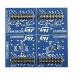


 工商网监
湘ICP备2023018690号
工商网监
湘ICP备2023018690号
