STL3NM60N
Datasheet
N-channel 600 V, 1.5 Ω typ., 2.2 A MDmesh II Power MOSFET
in a PowerFLAT 3.3x3.3 HV package
Features
12
87
6
3
4
56
5
7
•
•
•
8
Order code
VDS
RDS(on ) max.
ID
STL3NM60N
600 V
1.8 Ω
2.2 A
100% avalanche tested
Low input capacitance and gate charge
Low gate input resistance
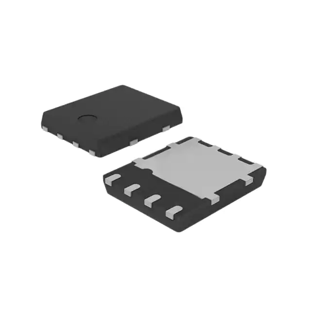
PowerFLAT 3.3x3.3 HV
Applications
•
Switching applications
D(5, 6, 7, 8)
Description
This device is an N-channel Power MOSFET developed using the second generation
of MDmesh technology. This revolutionary Power MOSFET associates a vertical
structure to the company’s strip layout to yield one of the world’s lowest on-resistance
and gate charge. It is therefore suitable for the most demanding high efficiency
converters.
G(4)
S(1, 2, 3)
AM15810v1
Product status link
STL3NM60N
Product summary
Order code
STL3NM60N
Marking
3NM60
Package
PowerFLAT 3.3x3.3 HV
Packing
Tape and reel
DS8889 - Rev 3 - May 2022
For further information contact your local STMicroelectronics sales office.
www.st.com
�STL3NM60N
Electrical ratings
1
Electrical ratings
Table 1. Absolute maximum ratings
Symbol
Parameter
Value
Unit
VDS
Drain-source voltage
600
V
VGS
Gate-source voltage
±25
V
Drain current (continuous) at TC = 25 °C
2.2
Drain current (continuous) at TC = 100 °C
1.7
Drain current (continuous) at TA = 25 °C
0.65
Drain current (continuous) at TA = 100 °C
0.5
Drain current pulsed
2.6
A
Total power dissipation at TA = 25 °C
2
W
Total power dissipation at TC = 25 °C
22
W
IAS
Avalanche current, repetitive or non-repetitive (pulse width limited by TJ max)
1
A
EAS
Single pulse avalanche energy (starting TJ = 25 °C, ID = IAS, VDD = 50 V)
119
mJ
Peak diode recovery voltage slope
15
V/ns
ID
IDM
(1)
PTOT
dv/dt(2)
TJ
Operating junction temperature range
Tstg
Storage temperature range
-55 to 150
A
°C
°C
1. Pulse width is limited by safe operating area.
2. ISD ≤ 2.2 A, di/dt ≤ 400 A/μs, VDS (peak) ≤ V(BR)DSS, VDD = 80% V(BR)DSS.
Table 2. Thermal data
Symbol
RthJC
(1)
RthJA
Parameter
Value
Unit
Thermal resistance, junction-to-case
5.6
°C/W
Thermal resistance, junction-to-ambient
62.5
°C/W
1. When mounted on an 1-inch² FR-4, 2 Oz copper board, t < 10 s .
DS8889 - Rev 3
page 2/13
�STL3NM60N
Electrical characteristics
2
Electrical characteristics
TC = 25 °C unless otherwise specified.
Table 3. On/off states
Symbol
V(BR)DSS
Parameter
Test conditions
Drain-source breakdown voltage
Min.
VGS = 0 V, ID = 1 mA
Typ.
600
Zero gate voltage drain current
IGSS
Gate-body leakage current
VDS = 0 V, VGS = ±25 V
VGS(th)
Gate threshold voltage
VDS = VGS, ID = 250 µA
RDS(on)
Static drain-source on-resistance
VGS = 10 V, ID = 1 A
VGS = 0 V, VDS = 600 V, TC = 125
Unit
V
VGS = 0 V, VDS = 600 V
IDSS
Max.
1
°C(1)
100
µA
±100
nA
3
4
V
1.5
1.8
Ω
Min.
Typ.
Max.
Unit
-
188
-
pF
-
13
-
pF
-
1.1
-
pF
2
1. Defined by design, not subject to production test.
Table 4. Dynamic
Symbol
Parameter
Ciss
Input capacitance
Coss
Output capacitance
Crss
Reverse transfer capacitance
Test conditions
VDS = 50 V, f = 1 MHz, VGS = 0 V
Equivalent capacitance energy
related
VDS = 0 to 480 V, VGS = 0 V
-
100
-
pF
RG
Intrinsic gate resistance
f = 1 MHz open drain
-
6
-
Ω
Qg
Total gate charge
VDD = 480 V, ID = 2.2 A
-
9.5
-
nC
Qgs
Gate-source charge
VGS = 0 to 10 V
-
1.6
-
nC
Qgd
Gate-drain charge
(see Figure 14. Test circuit for gate
charge behavior)
-
5.3
-
nC
Coss eq.(1)
1. Coss eq. is defined as a constant equivalent capacitance giving the same charging time as Coss when VDS increases from 0
to 80% VDSS.
Table 5. Switching times
Symbol
td(on)
tr
td(off)
tf
DS8889 - Rev 3
Parameter
Test conditions
Min.
Typ.
Max.
Unit
Turn-on delay time
VDD = 300 V, ID = 1.1 A,
-
8.6
-
ns
Rise time
RG = 4.7 Ω, VGS = 10 V
-
6.2
-
ns
Turn-off delay time
(see Figure 13. Test circuit for
resistive load switching times and
Figure 18. Switching time waveform)
-
20.8
-
ns
-
20
-
ns
Fall time
page 3/13
�STL3NM60N
Electrical characteristics
Table 6. Source-drain diode
Symbol
ISD
ISDM
(1)
VSD(2)
Parameter
Test conditions
Min.
Typ.
Max.
Unit
Source-drain current
-
2.2
A
Source-drain current (pulsed)
-
2.6
A
1.6
V
Forward on voltage
ISD = 2.2 A, VGS = 0 V
-
trr
Reverse recovery time
ISD = 2.2 A, di/dt = 100 A/µs,
-
168
ns
Qrr
Reverse recovery charge
VDD = 60 V
-
672
nC
IRRM
Reverse recovery current
(see Figure 15. Test circuit for inductive
load switching and diode recovery times)
-
8
A
trr
Reverse recovery time
ISD = 2.2 A, di/dt = 100 A/µs,
-
2.3
ns
Qrr
Reverse recovery charge
VDD = 60 V, TJ = 150 °C
-
913
nC
Reverse recovery current
(see Figure 15. Test circuit for inductive
load switching and diode recovery times)
-
9
A
IRRM
1. Pulse width is limited by safe operating area.
2. Pulsed: pulse duration = 300 µs, duty cycle 1.5%.
DS8889 - Rev 3
page 4/13
�STL3NM60N
Electrical characteristics (curves)
2.1
Electrical characteristics (curves)
Figure 1. Safe operating area
ID
(A) Operation in this area is
Figure 2. Normalized transient thermal impedance
AM11244v1
limited by RDS(on)
10 0
tp= 1ms
10
-1
tp= 10ms
tp= 100ms
10 -2
TJ ≤ 150 °C
TA= 25 °C
single pulse
10 0
10 1
VDS (V)
10 2
Figure 3. Typical output characteristics
AM11245v1
VGS =10V
5
Figure 4. Typical transfer characteristics
AM11246v1
ID
(A)
VDS =21V
5
4
4
6V
3
3
2
2
5V
1
0
RthJA
tp= 1s
10 -3
10 -1
ID
(A)
RthJA
5
0
10
15
20
25
30
1
VDS (V)
Figure 5. Typical gate charge characteristics
AM11247v1
VDS (V)
VGS
(V)
VDD=480V
ID=2.2A
12
500
VDS
10
400
2
0
4
6
8
10
VGS (V)
Figure 6. Typical drain-source on-resistance
AM11248v1
R DS (on)
(Ω)
1.58
VGS =10V
1.56
1.54
1.52
8
300
6
1.50
1.48
200
4
100
2
0
0
0
DS8889 - Rev 3
1.46
1.44
1.42
2
4
6
8
0
10 Q g (nC)
1.40
0
0.5
1
1.5
2
ID(A)
page 5/13
�STL3NM60N
Electrical characteristics (curves)
Figure 7. Typical capacitance characteristics
AM11249v1
C
(pF)
Figure 8. Typical output capacitance stored energy
AM11250v1
E os s
1000
Cis s
100
10
Cos s
1
0.1
1
100
10
Crs s
VDS (V)
Figure 9. Normalized gate threshold vs temperature
AM11252v1
VGS(th)
DS
Figure 10. Normalized on-resistance vs temperature
AM11253v1
R DS (on)
(norm)
(norm)
2.5
1.10
ID=250µA
VGS=10 V
2.1
1.00
1.7
0.90
1.3
0.80
0.70
-50
0.9
-25
0
25
50
75 100
TJ(°C)
Figure 11. Normalized breakdown voltage vs temperature
AM11251v1
V(BR)DSS
(norm)
0.5
-50 -25
0
25
50
75 100
TJ (°C)
Figure 12. Typical reverse diode forward characteristics
AM11254v1
VS D
1.4
1.07
ID=1mA
TJ =-50°C
1.05
J =25°C
1.03
1.01
TJ =150°C
0.99
0.97
0.95
0.93
-50 -25
DS8889 - Rev 3
0
25
50
75 100
TJ(°C)
0
1.0
IS D
page 6/13
�STL3NM60N
Test circuits
3
Test circuits
Figure 13. Test circuit for resistive load switching times
Figure 14. Test circuit for gate charge behavior
VDD
12 V
2200
+ μF
3.3
μF
VDD
VD
VGS
1 kΩ
100 nF
RL
IG= CONST
VGS
RG
47 kΩ
+
pulse width
D.U.T.
2.7 kΩ
2200
μF
pulse width
D.U.T.
100 Ω
VG
47 kΩ
1 kΩ
AM01469v1
AM01468v1
Figure 15. Test circuit for inductive load switching and
diode recovery times
D
G
A
D.U.T.
S
25 Ω
A
A
L
100 µH
fast
diode
B
B
B
G
RG
VD
3.3
µF
D
+
Figure 16. Unclamped inductive load test circuit
1000
+ µF
2200
+ µF
VDD
3.3
µF
VDD
ID
D.U.T.
S
_
D.U.T.
Vi
pulse width
AM01470v1
AM01471v1
Figure 17. Unclamped inductive waveform
Figure 18. Switching time waveform
ton
V(BR)DSS
td(on)
toff
td(off)
tr
tf
VD
90%
90%
IDM
VDD
VDD
VGS
0
AM01472v1
DS8889 - Rev 3
10%
0
ID
VDS
10%
90%
10%
AM01473v1
page 7/13
�STL3NM60N
Package information
4
Package information
In order to meet environmental requirements, ST offers these devices in different grades of ECOPACK packages,
depending on their level of environmental compliance. ECOPACK specifications, grade definitions and product
status are available at: www.st.com. ECOPACK is an ST trademark.
DS8889 - Rev 3
page 8/13
�STL3NM60N
PowerFLAT 3.3x3.3 HV package information
4.1
PowerFLAT 3.3x3.3 HV package information
Figure 19. PowerFLAT 3.3x3.3 HV package outline
.
8374983_Rev_2
DS8889 - Rev 3
page 9/13
�STL3NM60N
PowerFLAT 3.3x3.3 HV package information
Table 7. PowerFLAT 3.3x3.3 HV package mechanical data
Dim.
mm
Min.
Typ.
Max.
A
0.80
0.90
1.00
A1
0
0.02
0.05
b
0.25
0.30
0.40
D
D2
3.30
2.50
E
E2
2.75
3.30
1.15
e
L
2.65
1.30
1.40
0.65
0.20
0.30
aaa
0.10
bbb
0.10
ccc
0.10
ddd
0.05
eee
0.08
0.40
Figure 20. PowerFLAT 3.3x3.3 HV recommended footprint (dimensions are in mm)
8374983_footprint
DS8889 - Rev 3
page 10/13
�STL3NM60N
Revision history
Table 8. Document revision history
Date
Version
12-Mar-2012
1
Changes
First release.
Document status changed from preliminary to production data.
19-Nov-2014
2
Updated Figure 1.: Internal schematic diagram, Figure 2.: Safe operating area, Figure 3.:
Thermal impedance and Figure 12.: Normalized V(BR)DSS vs temperature.
Updated Table 5.: Dynamic and Table 7.: Source drain diode.
Minor text changes.
Modified marking on cover page
Updated Figure 1. Safe operating area
26-May-2022
3
Modified ISDM value in Table 6. Source-drain diode
Updated Section 4.1 PowerFLAT 3.3x3.3 HV package information
Minor text changes.
DS8889 - Rev 3
page 11/13
�STL3NM60N
Contents
Contents
1
Electrical ratings . . . . . . . . . . . . . . . . . . . . . . . . . . . . . . . . . . . . . . . . . . . . . . . . . . . . . . . . . . . . . . . . . .2
2
Electrical characteristics. . . . . . . . . . . . . . . . . . . . . . . . . . . . . . . . . . . . . . . . . . . . . . . . . . . . . . . . . . . 3
2.1
Electrical characteristics (curves) . . . . . . . . . . . . . . . . . . . . . . . . . . . . . . . . . . . . . . . . . . . . . . . . . 5
3
Test circuits . . . . . . . . . . . . . . . . . . . . . . . . . . . . . . . . . . . . . . . . . . . . . . . . . . . . . . . . . . . . . . . . . . . . . . .7
4
Package information. . . . . . . . . . . . . . . . . . . . . . . . . . . . . . . . . . . . . . . . . . . . . . . . . . . . . . . . . . . . . . .8
4.1
PowerFLAT 3.3x3.3 HV package information . . . . . . . . . . . . . . . . . . . . . . . . . . . . . . . . . . . . . . . 9
Revision history . . . . . . . . . . . . . . . . . . . . . . . . . . . . . . . . . . . . . . . . . . . . . . . . . . . . . . . . . . . . . . . . . . . . . . .11
DS8889 - Rev 3
page 12/13
�STL3NM60N
IMPORTANT NOTICE – READ CAREFULLY
STMicroelectronics NV and its subsidiaries (“ST”) reserve the right to make changes, corrections, enhancements, modifications, and improvements to ST
products and/or to this document at any time without notice. Purchasers should obtain the latest relevant information on ST products before placing orders. ST
products are sold pursuant to ST’s terms and conditions of sale in place at the time of order acknowledgment.
Purchasers are solely responsible for the choice, selection, and use of ST products and ST assumes no liability for application assistance or the design of
purchasers’ products.
No license, express or implied, to any intellectual property right is granted by ST herein.
Resale of ST products with provisions different from the information set forth herein shall void any warranty granted by ST for such product.
ST and the ST logo are trademarks of ST. For additional information about ST trademarks, refer to www.st.com/trademarks. All other product or service names
are the property of their respective owners.
Information in this document supersedes and replaces information previously supplied in any prior versions of this document.
© 2022 STMicroelectronics – All rights reserved
DS8889 - Rev 3
page 13/13
�


 工商网监
湘ICP备2023018690号
工商网监
湘ICP备2023018690号
