STM8T143
Single-channel capacitive sensor for touch and proximity detection
Datasheet - production data
Applications
• Ear-face proximity detection for smart phone
devices
SO8
(narrow)
• Companion device for navigation
joystick/optical track pad
UFDFPN8
(2 x 3 mm)
• User hand detection for Nomad equipment
(tablet PC)
• Ear-head detection for MP3/walkman ear buds
and Bluetooth headsets
Features
• Touch and short range proximity detection
• On/off touch sensing button such as GPS
system home button
• Internal sampling capacitor
• User hands detection for mouse/keyboards
• On-chip integrated voltage regulator
• Wall switch backlight activation on user
approach and light controls on user touch
• Automatic electrode tuning (AET)
• Electrode parasitic capacitance compensation
(EPCC)
• Dynamic calibration (DYCAL™)
• Environment control system (ECS)
• User programmable options include:
• Configurable output modes
• Configurable sensitivity levels
• Data streaming mode
• Low power management
• Operating supply voltage: 2.3 V to 5.5 V
• Supported interface:
– Individual key state output
– Single wire data interface
• Operating temperature: -40 to +85 °C
• ECOPACK®2 8-pin SO and 8-pin UFDFPN
packages
January 2014
This is information on a product in full production.
DocID18315 Rev 7
1/65
www.st.com
�Contents
STM8T143
Contents
1
Description . . . . . . . . . . . . . . . . . . . . . . . . . . . . . . . . . . . . . . . . . . . . . . . . . 7
2
Block diagram . . . . . . . . . . . . . . . . . . . . . . . . . . . . . . . . . . . . . . . . . . . . . . 8
3
Pin descriptions . . . . . . . . . . . . . . . . . . . . . . . . . . . . . . . . . . . . . . . . . . . . 9
4
STM8T ProxSense technology . . . . . . . . . . . . . . . . . . . . . . . . . . . . . . . . 11
5
4.1
Capacitive sensing overview . . . . . . . . . . . . . . . . . . . . . . . . . . . . . . . . . . .11
4.2
Charge-transfer acquisition principle . . . . . . . . . . . . . . . . . . . . . . . . . . . . .11
4.3
Internal sampling capacitor . . . . . . . . . . . . . . . . . . . . . . . . . . . . . . . . . . . 13
4.4
Electrode parasitic capacitance compensation (EPCC) . . . . . . . . . . . . . . 13
STM8T143 processing . . . . . . . . . . . . . . . . . . . . . . . . . . . . . . . . . . . . . . 14
5.1
Automatic electrode tuning (AET) . . . . . . . . . . . . . . . . . . . . . . . . . . . . . . 14
5.2
Signal calculation and reference calibration . . . . . . . . . . . . . . . . . . . . . . . 15
5.3
Detection and release thresholds . . . . . . . . . . . . . . . . . . . . . . . . . . . . . . . 16
5.4
Dynamic calibration (DYCAL) . . . . . . . . . . . . . . . . . . . . . . . . . . . . . . . . . . 18
5.5
Environment control system (ECS) . . . . . . . . . . . . . . . . . . . . . . . . . . . . . 21
5.6
6
2/65
5.5.1
ECS principle . . . . . . . . . . . . . . . . . . . . . . . . . . . . . . . . . . . . . . . . . . . . . 21
5.5.2
ECS halt . . . . . . . . . . . . . . . . . . . . . . . . . . . . . . . . . . . . . . . . . . . . . . . . . 22
5.5.3
Reference freeze and reference freeze timeout . . . . . . . . . . . . . . . . . . 23
5.5.4
ECS filter constant adjustment . . . . . . . . . . . . . . . . . . . . . . . . . . . . . . . 24
Debounce filter . . . . . . . . . . . . . . . . . . . . . . . . . . . . . . . . . . . . . . . . . . . . . 25
Device operation . . . . . . . . . . . . . . . . . . . . . . . . . . . . . . . . . . . . . . . . . . . 26
6.1
Option byte description . . . . . . . . . . . . . . . . . . . . . . . . . . . . . . . . . . . . . . . 26
6.2
Device operating modes . . . . . . . . . . . . . . . . . . . . . . . . . . . . . . . . . . . . . . 29
6.2.1
Dual output mode . . . . . . . . . . . . . . . . . . . . . . . . . . . . . . . . . . . . . . . . . 29
6.2.2
Control mode . . . . . . . . . . . . . . . . . . . . . . . . . . . . . . . . . . . . . . . . . . . . . 30
6.2.3
Data streaming mode . . . . . . . . . . . . . . . . . . . . . . . . . . . . . . . . . . . . . . 31
6.3
Output polarity . . . . . . . . . . . . . . . . . . . . . . . . . . . . . . . . . . . . . . . . . . . . . 32
6.4
Power modes . . . . . . . . . . . . . . . . . . . . . . . . . . . . . . . . . . . . . . . . . . . . . . 33
DocID18315 Rev 7
�STM8T143
Contents
7
Typical application diagram . . . . . . . . . . . . . . . . . . . . . . . . . . . . . . . . . . 34
8
Design guidelines . . . . . . . . . . . . . . . . . . . . . . . . . . . . . . . . . . . . . . . . . . 36
8.1
Sensitivity adjustment . . . . . . . . . . . . . . . . . . . . . . . . . . . . . . . . . . . . . . . . 36
8.1.1
9
Electrical characteristics . . . . . . . . . . . . . . . . . . . . . . . . . . . . . . . . . . . . 37
9.1
10
Parameter conditions . . . . . . . . . . . . . . . . . . . . . . . . . . . . . . . . . . . . . . . . 37
9.1.1
Minimum and maximum values . . . . . . . . . . . . . . . . . . . . . . . . . . . . . . . 37
9.1.2
Typical values . . . . . . . . . . . . . . . . . . . . . . . . . . . . . . . . . . . . . . . . . . . . 37
9.1.3
Typical curves . . . . . . . . . . . . . . . . . . . . . . . . . . . . . . . . . . . . . . . . . . . . 37
9.1.4
Loading capacitor . . . . . . . . . . . . . . . . . . . . . . . . . . . . . . . . . . . . . . . . . 37
9.2
Absolute maximum ratings . . . . . . . . . . . . . . . . . . . . . . . . . . . . . . . . . . . . 38
9.3
Operating conditions . . . . . . . . . . . . . . . . . . . . . . . . . . . . . . . . . . . . . . . . 38
9.3.1
General operating conditions and supply characteristics . . . . . . . . . . . 38
9.3.2
Average current consumption . . . . . . . . . . . . . . . . . . . . . . . . . . . . . . . . 39
9.3.3
I/O pin characteristics . . . . . . . . . . . . . . . . . . . . . . . . . . . . . . . . . . . . . . 39
9.4
Regulator and reference voltage . . . . . . . . . . . . . . . . . . . . . . . . . . . . . . . 41
9.5
Capacitive sensing characteristics . . . . . . . . . . . . . . . . . . . . . . . . . . . . . . 42
9.6
Streaming mode characteristics . . . . . . . . . . . . . . . . . . . . . . . . . . . . . . . . 44
9.7
EMC characteristics . . . . . . . . . . . . . . . . . . . . . . . . . . . . . . . . . . . . . . . . . 45
9.7.1
Functional EMS (electromagnetic susceptibility) . . . . . . . . . . . . . . . . . . 45
9.7.2
Prequalification trials . . . . . . . . . . . . . . . . . . . . . . . . . . . . . . . . . . . . . . . 45
9.7.3
Electromagnetic interference (EMI) . . . . . . . . . . . . . . . . . . . . . . . . . . . . 45
9.7.4
Absolute maximum ratings (electrical sensitivity) . . . . . . . . . . . . . . . . . 46
9.7.5
Electrostatic discharge (ESD) . . . . . . . . . . . . . . . . . . . . . . . . . . . . . . . . 46
9.7.6
Static latchup . . . . . . . . . . . . . . . . . . . . . . . . . . . . . . . . . . . . . . . . . . . . . 46
Package characteristics . . . . . . . . . . . . . . . . . . . . . . . . . . . . . . . . . . . . . 47
10.1
10.2
Package mechanical data . . . . . . . . . . . . . . . . . . . . . . . . . . . . . . . . . . . . 48
10.1.1
SO8 package mechanical data . . . . . . . . . . . . . . . . . . . . . . . . . . . . . . . 48
10.1.2
UFDFPN8 package mechanical data . . . . . . . . . . . . . . . . . . . . . . . . . . . 50
Package thermal characteristics . . . . . . . . . . . . . . . . . . . . . . . . . . . . . . . 52
10.2.1
11
PCB layout and construction . . . . . . . . . . . . . . . . . . . . . . . . . . . . . . . . . 36
Reference document . . . . . . . . . . . . . . . . . . . . . . . . . . . . . . . . . . . . . . . 52
Ordering information . . . . . . . . . . . . . . . . . . . . . . . . . . . . . . . . . . . . . . . 53
DocID18315 Rev 7
3/65
4
�Contents
STM8T143
11.1
STM8T143 ordering information scheme . . . . . . . . . . . . . . . . . . . . . . . . . 53
11.2
Orderable favorite device lists . . . . . . . . . . . . . . . . . . . . . . . . . . . . . . . . . 54
11.2.1
Part number option bytes . . . . . . . . . . . . . . . . . . . . . . . . . . . . . . . . . . . . 54
11.3
In-factory option byte programming service . . . . . . . . . . . . . . . . . . . . . . . 54
11.4
Revision code on device markings . . . . . . . . . . . . . . . . . . . . . . . . . . . . . . 55
12
STM8T143 programming tool . . . . . . . . . . . . . . . . . . . . . . . . . . . . . . . . . 59
13
Revision history . . . . . . . . . . . . . . . . . . . . . . . . . . . . . . . . . . . . . . . . . . . 60
4/65
DocID18315 Rev 7
�STM8T143
List of tables
List of tables
Table 1.
Table 2.
Table 3.
Table 4.
Table 5.
Table 6.
Table 7.
Table 8.
Table 9.
Table 10.
Table 11.
Table 12.
Table 13.
Table 14.
Table 15.
Table 16.
Table 17.
Table 18.
Table 19.
Table 20.
Table 21.
Table 22.
Table 23.
Table 24.
Table 25.
Table 26.
Table 27.
Table 28.
Table 29.
Table 30.
Table 31.
STM8T143 pin descriptions . . . . . . . . . . . . . . . . . . . . . . . . . . . . . . . . . . . . . . . . . . . . . . . . 10
Option bytes . . . . . . . . . . . . . . . . . . . . . . . . . . . . . . . . . . . . . . . . . . . . . . . . . . . . . . . . . . . . 26
Option byte description . . . . . . . . . . . . . . . . . . . . . . . . . . . . . . . . . . . . . . . . . . . . . . . . . . . . 27
Pin 1 configuration . . . . . . . . . . . . . . . . . . . . . . . . . . . . . . . . . . . . . . . . . . . . . . . . . . . . . . . 29
Pin 8 configuration . . . . . . . . . . . . . . . . . . . . . . . . . . . . . . . . . . . . . . . . . . . . . . . . . . . . . . . 29
Data streaming frame . . . . . . . . . . . . . . . . . . . . . . . . . . . . . . . . . . . . . . . . . . . . . . . . . . . . . 32
Voltage characteristics . . . . . . . . . . . . . . . . . . . . . . . . . . . . . . . . . . . . . . . . . . . . . . . . . . . . 38
Current characteristics . . . . . . . . . . . . . . . . . . . . . . . . . . . . . . . . . . . . . . . . . . . . . . . . . . . . 38
Thermal characteristics. . . . . . . . . . . . . . . . . . . . . . . . . . . . . . . . . . . . . . . . . . . . . . . . . . . . 38
Operating characteristics . . . . . . . . . . . . . . . . . . . . . . . . . . . . . . . . . . . . . . . . . . . . . . . . . . 38
Average current consumption . . . . . . . . . . . . . . . . . . . . . . . . . . . . . . . . . . . . . . . . . . . . . . . 39
OUT/TOUT/DATA streaming pin characteristics . . . . . . . . . . . . . . . . . . . . . . . . . . . . . . . . 39
POUT/TOUT pin characteristics . . . . . . . . . . . . . . . . . . . . . . . . . . . . . . . . . . . . . . . . . . . . . 40
CTRL pin characteristics. . . . . . . . . . . . . . . . . . . . . . . . . . . . . . . . . . . . . . . . . . . . . . . . . . . 40
Regulator and reference voltage . . . . . . . . . . . . . . . . . . . . . . . . . . . . . . . . . . . . . . . . . . . . 41
General capacitive sensing characteristics. . . . . . . . . . . . . . . . . . . . . . . . . . . . . . . . . . . . . 42
Internal CS value. . . . . . . . . . . . . . . . . . . . . . . . . . . . . . . . . . . . . . . . . . . . . . . . . . . . . . . . . 43
Implemented EPCC values (pF) . . . . . . . . . . . . . . . . . . . . . . . . . . . . . . . . . . . . . . . . . . . . . 44
External sensing component characteristics . . . . . . . . . . . . . . . . . . . . . . . . . . . . . . . . . . . 44
Data streaming timing characteristics . . . . . . . . . . . . . . . . . . . . . . . . . . . . . . . . . . . . . . . . . 44
EMS data . . . . . . . . . . . . . . . . . . . . . . . . . . . . . . . . . . . . . . . . . . . . . . . . . . . . . . . . . . . . . . 45
EMI data . . . . . . . . . . . . . . . . . . . . . . . . . . . . . . . . . . . . . . . . . . . . . . . . . . . . . . . . . . . . . . . 45
ESD absolute maximum ratings . . . . . . . . . . . . . . . . . . . . . . . . . . . . . . . . . . . . . . . . . . . . . 46
Electrical sensitivities . . . . . . . . . . . . . . . . . . . . . . . . . . . . . . . . . . . . . . . . . . . . . . . . . . . . . 46
SO8-lead plastic small outline - package mechanical data. . . . . . . . . . . . . . . . . . . . . . . . . 48
UFDFPN8-lead ultra thin fine pitch dual flat - package mechanical data . . . . . . . . . . . . . . 50
Thermal characteristics. . . . . . . . . . . . . . . . . . . . . . . . . . . . . . . . . . . . . . . . . . . . . . . . . . . . 52
Option byte values . . . . . . . . . . . . . . . . . . . . . . . . . . . . . . . . . . . . . . . . . . . . . . . . . . . . . . . 54
Device identification . . . . . . . . . . . . . . . . . . . . . . . . . . . . . . . . . . . . . . . . . . . . . . . . . . . . . . 55
Ordering information . . . . . . . . . . . . . . . . . . . . . . . . . . . . . . . . . . . . . . . . . . . . . . . . . . . . . . 59
Document revision history . . . . . . . . . . . . . . . . . . . . . . . . . . . . . . . . . . . . . . . . . . . . . . . . . 60
DocID18315 Rev 7
5/65
5
�List of figures
STM8T143
List of figures
Figure 1.
Figure 2.
Figure 3.
Figure 4.
Figure 5.
Figure 6.
Figure 7.
Figure 8.
Figure 9.
Figure 10.
Figure 11.
Figure 12.
Figure 13.
Figure 14.
Figure 15.
Figure 16.
Figure 17.
Figure 18.
Figure 19.
Figure 20.
Figure 21.
Figure 22.
Figure 23.
Figure 24.
Figure 25.
Figure 26.
Figure 27.
Figure 28.
Figure 29.
6/65
STM8T143 block diagram. . . . . . . . . . . . . . . . . . . . . . . . . . . . . . . . . . . . . . . . . . . . . . . . . . . 8
SO8 pinout . . . . . . . . . . . . . . . . . . . . . . . . . . . . . . . . . . . . . . . . . . . . . . . . . . . . . . . . . . . . . . 9
UFDFPN8 pinout . . . . . . . . . . . . . . . . . . . . . . . . . . . . . . . . . . . . . . . . . . . . . . . . . . . . . . . . . 9
Coupling with hand increases the capacitance of the sensing electrode . . . . . . . . . . . . . . 11
STM8T143 measuring circuitry . . . . . . . . . . . . . . . . . . . . . . . . . . . . . . . . . . . . . . . . . . . . . . 12
Signal monitored on CX pin. . . . . . . . . . . . . . . . . . . . . . . . . . . . . . . . . . . . . . . . . . . . . . . . . 12
Automatic electrode tuning (AET) . . . . . . . . . . . . . . . . . . . . . . . . . . . . . . . . . . . . . . . . . . . . 15
Signal reference and detection threshold (not detailed) . . . . . . . . . . . . . . . . . . . . . . . . . . . 17
DYCAL general operation . . . . . . . . . . . . . . . . . . . . . . . . . . . . . . . . . . . . . . . . . . . . . . . . . . 18
DYCAL operation with water residue . . . . . . . . . . . . . . . . . . . . . . . . . . . . . . . . . . . . . . . . . 19
No DYCAL . . . . . . . . . . . . . . . . . . . . . . . . . . . . . . . . . . . . . . . . . . . . . . . . . . . . . . . . . . . . . 20
IIR filter formula . . . . . . . . . . . . . . . . . . . . . . . . . . . . . . . . . . . . . . . . . . . . . . . . . . . . . . . . . 21
ECS halt . . . . . . . . . . . . . . . . . . . . . . . . . . . . . . . . . . . . . . . . . . . . . . . . . . . . . . . . . . . . . . . 22
Unwanted detection managed by the reference freeze timeout . . . . . . . . . . . . . . . . . . . . . 23
ECS filter K constant management. . . . . . . . . . . . . . . . . . . . . . . . . . . . . . . . . . . . . . . . . . . 24
Data streaming frame . . . . . . . . . . . . . . . . . . . . . . . . . . . . . . . . . . . . . . . . . . . . . . . . . . . . . 31
Typical application schematic for Control mode . . . . . . . . . . . . . . . . . . . . . . . . . . . . . . . . . 34
Typical application schematic for Dual output mode . . . . . . . . . . . . . . . . . . . . . . . . . . . . . 34
Typical application schematic for Data streaming mode. . . . . . . . . . . . . . . . . . . . . . . . . . . 35
Pin loading conditions . . . . . . . . . . . . . . . . . . . . . . . . . . . . . . . . . . . . . . . . . . . . . . . . . . . . . 37
Data streaming timing diagram . . . . . . . . . . . . . . . . . . . . . . . . . . . . . . . . . . . . . . . . . . . . . . 44
SO8-lead plastic small outline - package outline . . . . . . . . . . . . . . . . . . . . . . . . . . . . . . . . 48
SO8 narrow recommended footprint (dimensions in mm) . . . . . . . . . . . . . . . . . . . . . . . . . 49
UFDFPN8-lead ultra thin fine pitch dual flat package (MLP) package outline . . . . . . . . . . 50
UFDFPN 2 x 3 mm recommended footprint (dimensions in mm) . . . . . . . . . . . . . . . . . . . . 51
STM8T143 ordering information scheme . . . . . . . . . . . . . . . . . . . . . . . . . . . . . . . . . . . . . . 53
SO8 package marking . . . . . . . . . . . . . . . . . . . . . . . . . . . . . . . . . . . . . . . . . . . . . . . . . . . . 55
UFDFPN8 package marking . . . . . . . . . . . . . . . . . . . . . . . . . . . . . . . . . . . . . . . . . . . . . . . . 56
STM8T143 programming tool . . . . . . . . . . . . . . . . . . . . . . . . . . . . . . . . . . . . . . . . . . . . . . . 59
DocID18315 Rev 7
�STM8T143
1
Description
Description
The STM8T143 is a single channel, fully integrated, touch sensing capacitive sensor. It uses
a ProxSense™ charge transfer capacitive acquisition method that is capable of near range
proximity detection. The STM8T143 offers a state of the art capacitive sensing engine with
an embedded sampling capacitor and voltage regulator allowing the overall solution cost to
be reduced and improving system immunity in noisy environments. It can target a detection
range up to 20 cm thanks to the electrode parasitic capacitance compensation (EPCC)
feature. The EPCC automatically compensates ground parasitic capacitance sources (such
as ground planes, printed circuit board tacks, and large metal objects) which significantly
reduce the proximity detection range.
The application fields or typical functions with proximity features are various and include:
on/off switches, replacement/enhancement, home buttons, backlighting feature on proximity
for user interfaces, wakeup or control function on proximity, find-in-the-dark for lighting
equipment, and companion device for battery saving in portable equipment.
The device has been designed to be used in applications where proximity is required and
touch conditions can prevail for an extended period of time which may result in
uncompensated drift in conventional capacitive sensors. Therefore, a process called
DYCAL is implemented.
The STM8T143 is an ideal alternative, cost-effective, and extremely low power solution to
replace conventional infrared optical proximity sensors. Capacitive sensing technology is
not sensitive to sunlight or artificial light effects. The STM8T143 offers a much lower
consumption (12 µA range versus 100 µA range) and a small form factor (DFN8 2*3*0.65
mm). Lastly, there is no need for a clear opening on the bezel to let light pass through.
The STM8T143 is offered in 8-pin packages and features both touch and proximity sensing
outputs.
The STM8T143 touch pad can sense through almost any dielectric and thereby allows the
electronics to be contained in a sealed enclosure.
Note:
ProxSense™ is a trademark of Azoteq (Pty) Ltd.
DocID18315 Rev 7
7/65
64
�Block diagram
2
STM8T143
Block diagram
Figure 1. STM8T143 block diagram
9ROWDJH
UHJXODWRU
9''
95(*
&RPSDUDWRU
$QDORJ
VZLWFK
&XUUHQW
PLUURU
287�7287�'$7$
&75/�3287
0&8�V\VWHP
HQJLQH
5&
RVF
975,3
2SWLRQ
E\WH
&6
9DULDEOH
QHJDWLYH
FDSDFLWDQFH
&;
&(3&&
$GYDQFHG�3UR[6HQVH�HQJLQH����
DL�����F
RC oscillator
The 1-MHz RC oscillator is an internal fixed frequency oscillator used to supply the clock to
the MCU system engine.
Voltage regulator
The voltage regulator has an internal comparison and feedback circuit that ensures the
VREG voltage is kept stable and constant. The regulator requires an external smoothing
capacitor.
MCU system engine
The MCU system engine controls the capacitive sensing engine and processes touch and
proximity detection signals.
Advanced ProxSense engine
The advanced ProxSense engine circuitry uses a charge-transfer method to detect
capacitance changes. It features:
8/65
•
An analog voltage comparator
•
A programmable internal sampling capacitor
•
A system that allows the ground parasitic capacitance to be compensated to improve
the system sensitivity. This system is called electrode parasitic capacitance
compensation (EPCC).
DocID18315 Rev 7
�STM8T143
3
Pin descriptions
Pin descriptions
Figure 2. SO8 pinout
287����7287����'$7$���
�
�
&75/����3287���
966
�
�
95(*
1&
�
�
1&
&;
�
�
9''
DL�����H
Figure 3. UFDFPN8 pinout
287����7287����'$7$���
�
�
&75/����3287���
966
�
�
95(*
1&
�
�
1&
&;
�
�
9''
DL�����H
1. Control mode
2. Dual output mode
3. Data streaming mode
DocID18315 Rev 7
9/65
64
�Pin descriptions
STM8T143
Table 1. STM8T143 pin descriptions
Pin
no.
Mode
Pin type(1)
Pin name
Pin function(2)
Control mode
OD/PP
OUT
Touch or proximity output
Dual output mode
OD/PP
TOUT
Touch output
Data streaming mode
OD
DATA
Data streaming output
2
-
S
VSS
Ground
3
-
-
NC
Not connected
4
-
SNS
CX
Capacitive sensing channel pin to RX
5
-
S
VDD
Supply voltage
6
-
-
NC
Not connected
7
-
S
VREG
Internal voltage regulator output(3)
Control mode
I
CTRL
Control input
Dual output mode
PP
POUT
Proximity output
1
8
1. S: power supply, SNS: capacitive sensing, OD: output open drain, PP: output push-pull, and I: input
2. Pin function depends on option byte configuration (please refer to Section 6: Device operation)
3. Requires a low equivalent series resistance (ESR), 1µF capacitor to ground. This output must not be used
to power other devices.
10/65
DocID18315 Rev 7
�STM8T143
STM8T ProxSense technology
4
STM8T ProxSense technology
4.1
Capacitive sensing overview
A capacitance exists between any reference point and ground as long as they are
electrically isolated. If this reference point is a sensing electrode, it can help to think of it as
a capacitor. The positive electrode of the capacitor is the sensing electrode, and the
negative electrode is formed by the surrounding area (virtual ground reference in Figure 4).
Figure 4. Coupling with hand increases the capacitance of the sensing electrode
Sensing electrode
CT
CX
Lower capacitance
Higher capacitance
When a conductive object is brought into proximity of the sensing electrode, coupling
appears between them, and the capacitance of the sensing electrode relative to ground
increases. For example, a human hand raises the capacitance of the sensing electrode as it
approaches it. Touching the dielectric panel that protects the electrode increases its
capacitance significantly.
4.2
Charge-transfer acquisition principle
To measure changes in the electrode capacitance, STM8T devices employ bursts of
charge-transfer cycles.
The measuring circuitry is connected to the CX pin. It is composed of a serial resistor RX
plus the sensing electrode itself of equivalent capacitance CX (see Figure 5). The sensing
electrode can be made of any electrically conductive material, such as copper on PCBs, or
transparent conductive material like Indium Tin Oxide (ITO) deposited on glass or Plexiglas.
The dielectric panel usually provides a high degree of isolation to prevent electrostatic
discharge (ESD) from reaching the STM8T touch sensing controller. Connecting the serial
resistor (RX) to the CX pin improves ESD immunity even more.
DocID18315 Rev 7
11/65
64
�STM8T ProxSense technology
STM8T143
Figure 5. STM8T143 measuring circuitry
# 4�^�P&
3ERIALRESISTOR�28
8
��
%ARTH
#8
$EVICE
#8
�^��P&
AI�����C
1. RX must be placed as close as possible to the device.
The principle of charge transfer is to charge the electrode capacitance (CX) using a stable
power supply. When CX is fully charged, part of the accumulated charge is transferred from
CX to an internal sampling capacitance, referred to as CS. The transfer cycle is repeated
until the voltage across the sampling capacitor CS reaches the end of acquisition reference
voltage (VTRIP). The change in the electrode capacitance, caused by the presence or
absence of the human body, is detected by measuring the number of transfer cycles
composing a burst (see Figure 6).
Throughout this document the following naming conventions apply:
•
The charge transfer period (tTRANSFER) refers to the charging of CX and the
subsequent transfer of the charge to CS.
•
The burst cycle duration (tBURST) is the time required to charge CS to VTRIP. The burst
count is the number of charge transfer periods (tTRANSFER) during one tBURST cycle.
•
The sampling period (tSAMPLING) is the acquisition rate.
Figure 6. Signal monitored on CX pin
T
#
42!.3&%2
8
T
"5234
73&(
6
#8,
T
"5234
T
3!-0,).'
T
!I�����
12/65
DocID18315 Rev 7
�STM8T143
4.3
STM8T ProxSense technology
Internal sampling capacitor
To reduce the application cost and increase the device flexibility, the STM8T143 features
several internal sampling capacitors to fit a wide range of applications.
4.4
Electrode parasitic capacitance compensation (EPCC)
The implementation of an electrode pad in a system always induces parasitic capacitances
through tracks and surrounding components.The electrode parasitic capacitance is the
residual capacitance between electrode and ground when no finger is present.
The EPCC is an internal hardware circuitry that compensates part of the electrode parasitic
capacitance to improve the capacitive sensing channel sensitivity.
DocID18315 Rev 7
13/65
64
�STM8T143 processing
5
STM8T143
STM8T143 processing
The STM8T143 device is designed to ensure reliable operation whatever the environment
and operating conditions. To achieve this high level of robustness, dedicated processing
have been implemented:
5.1
•
Automatic electrode tuning (AET)
•
Signal and reference calibration
•
Detection and release thresholds
•
Dynamic calibration (DYCAL)
•
Environment control system (ECS)
•
Debounce filter
•
Host control input
Automatic electrode tuning (AET)
AET is a sophisticated technology implemented in the STM8T143 device. It optimizes the
performance of the device in a wide range of applications and environmental conditions.
AET algorithm automatically adjusts the internal CS capacitor and EPCC parameters to
optimize system performance. Please refer to:
•
Table 17: Internal CS value for possible resulting values of this internal sampling
capacitance
•
Table 18: Implemented EPCC values (pF) for possible values of the EPCC
capacitance.
The principle is to select an internal CS capacitor and EPCC to obtain a burst count in a
predefined range of AET target value ± 256 burst counts.
At device startup, CS is selected to reach the nearest signal burst count value to a “gain
target value”. Then, the EPCC hardware subtracts an increasing capacitance value until a
“AET target value” is reached. During normal device operation, the EPCC hardware
subtracts from the electrode capacitance (CX), the compensation capacitance value
determined during the calibration phase.
This automatic system adaptation allows the same burst count number to be reached
regardless of the application electrode and surrounding.
The AET gain can be adjusted by selecting the gain target value through the “Gain target”
option bits.
The AET algorithm is executed whenever the device starts-up and during device operation
when the reference exits burst count range.
During the AET processing (tAET), proximity and touch events cannot be detected (please
refer to Table 6: Data streaming frame). In Data streaming mode, the AET activity is
reported and the internal CS and EPCC values can be monitored (see Section 6.2.3: Data
streaming mode).
14/65
DocID18315 Rev 7
�STM8T143
STM8T143 processing
Figure 7. Automatic electrode tuning (AET)
5HIHUHQFH�
�EXUVW�FRXQW�
7KHQ��WKH�(3&&�YDOXH�LV�
VHOHFWHG�WKURXJK�D�GLFKRWRP\�
DOJRULWKP�XQWLO�WKH�EXUVW�FRXQW�
UHDFKHV�WKH�$(7�WDUJHW�YDOXH
$(7
)LUVW��WKH�&6�YDOXH�LV�LQFUHDVHG�XQWLO�
WKH�EXUVW�FRXQW�UHDFKHV�WKH�JDLQ�
WDUJHW�YDOXH�VHOHFWHG�E\�RSWLRQ�E\WHV
*DLQ
��ELWV�&6�VHOHFWLRQ�
�&(3&&�VHW�WR���
��ELWV�
&(3&&�
VHOHFWLRQ
W
DL�����E
1. For the AET and gain target values, please refer to Table 16: General capacitive sensing characteristics.
5.2
Signal calculation and reference calibration
The capacitance change, induced by the presence of a finger or a hand in the device
detection area, is sensed by the variation in the number of charge transfer pulses
composing the burst. The number of charge transfer pulses is called “burst count”. The burst
count is filtered against the noise and compared to a “reference” to determine if there is a
touch/proximity detection. Please refer to Section 5.5: Environment control system (ECS)
for more details about the filtering process.
The reference is calculated at device startup during the calibration phase by averaging the
first 44 measurements before normal device operation.
Then, the environment control system takes care of the reference slow evolution over time.
DocID18315 Rev 7
15/65
64
�STM8T143 processing
5.3
STM8T143
Detection and release thresholds
During the detection operation, after calibration is over, the STM8T143 switches between
three operating states: no detection, proximity detection, and touch detection. The switch
between these states is driven by the difference between the signal and the reference.
The system goes from no detection to proximity detection state when the (reference - signal)
is higher than the proximity threshold (PTh). In this state, the ECS is halted and the
reference is frozen.
The system goes from no detection or proximity detection state to touch detection state
when the (reference - signal) is higher than the touch threshold (TTh). When this happens,
the reference value is changed to reflect the touch state after the delay tDYCAL. This process
is called dynamic calibration (DYCAL).
The system goes from the touch detection to no detection state when the (signal reference) goes above the release threshold (RTh). At this point, another DYCAL occurs for
the reference to represent the untouched state again.
For higher flexibility, several proximity and touch detection thresholds are available and
independently selectable through option byte: one PTh and one TTh.
•
The touch thresholds allow the touch sensitivity to be adapted to the panel thickness
and the electrode sensitivity.
•
The proximity thresholds allow the STM8T143 device to adapt to various surroundings
and to tune the detection distance.
The release threshold is a ratio of the touch threshold noted (TTh). TTh is selected by the
“touch detection threshold” option bits. The ratio is selected by the “release threshold ratio”
option bits.
A time filtering, similar to the debouncing of the mechanical switches, is applied to avoid
noise induced detections.
Please refer to Section 5.6: Debounce filter for operation details.
Figure 8 simplifies the proximity and touch detection event according to the signal variation
“Δ (signal)”. The Δ (signal) is the absolute value of the reference minus the signal.
16/65
DocID18315 Rev 7
�STM8T143
STM8T143 processing
Figure 8. Signal reference and detection threshold (not detailed)
2EFERENCE
3IGNAL
04H
44H
24H
T
$9#!,
T
0ROXIMITY
$ETECTION
4OUCH
$�SIGNAL �
2EF
3IGNAL
!%4?(!,4
$ETECTION
04H�
$�SIGNAL
$ �SIGNAL �44H
24H� $ �SIGNAL
$�SIGNAL
�24H
04H�
$�SIGNAL
�44H
AI�����
1. tAET_HALT = AET halt period after end of detection.
DocID18315 Rev 7
17/65
64
�STM8T143 processing
5.4
STM8T143
Dynamic calibration (DYCAL)
The STM8T143 DYCAL process is based on a dynamic threshold and reference
management which allows tracking of slow environmental changes even when the sensor is
in touch state. A low threshold is used to detect the proximity of an object, with a higher
threshold for touch detection. DYCAL is performed when a touch condition is detected for
longer than a certain period (tDYCAL). When a release condition occurs, the DYCAL
operation is performed instantaneously. Figure 9 represents the DYCAL operation for the
touch event (DYCAL_T) and for the release event (DYCAL_R).
After the DYCAL_R event, the AET process is frozen for a tAET_HALT delay.
Figure 9. DYCAL general operation
$9#!,?4
$9#!,?2
2EFERENCE
3IGNAL
04H
44H
24H��
4&4H��
T $9#!,
0ROXIMITY
OUTPUT
T !%4?(!,4��
$ETECTION
4OUCH
OUTPUT
$ETECTION
AI�����C
1. tAET_HALT = AET halt period after end of detection.
2. The release threshold (RTh) is a ratio of the touch threshold (TTh). TTh is selected by the “touch detection
threshold” option bits (TTh). The ratio is selected by the “release threshold ratio” option bits.
3. TFTh = Touch freeze threshold. Please refer to Table 16: General capacitive sensing characteristics and
Figure 12: IIR filter formula for the TFTh description.
4. In touch condition, the ECS allows the reference to adapt a slow signal variation change.
18/65
DocID18315 Rev 7
�STM8T143
STM8T143 processing
Figure 10 is an example of how the system behaves with a water residue when it is
managed by DYCAL.
Figure 10. DYCAL operation with water residue
$9#!,?4
$9#!,?2
2EFERENCE
3IGNAL
04H
04H
44H
44H
24H
4&4H��
T $9#!,
0ROXIMITY
OUTPUT
4OUCH
OUTPUT
T !%4?(!,4��
$ETECTION
$ETECTION
AI�����C
1. tAET_HALT = AET halt period after end of detection.
2. TFTh = Touch freeze threshold. Please refer to Table 16: General capacitive sensing characteristics and
Figure 12: IIR filter formula for the TFTh description.
DocID18315 Rev 7
19/65
64
�STM8T143 processing
STM8T143
Figure 11 is an example of how the system behaves with a water residue if the system is not
managed by DYCAL.
Figure 11. No DYCAL
2EFERENCE
3IGNAL
04H
44H
0ROXIMITY
OUTPUT
4OUCH
OUTPUT
0ROXIMITYDETECTIONISLOCKED/.
�
$ETECTION
AI�����
20/65
DocID18315 Rev 7
�STM8T143
STM8T143 processing
5.5
Environment control system (ECS)
5.5.1
ECS principle
The acquired signal value of the capacitive sensing channel increases or decreases
according to environmental conditions such as temperature, power supply, moisture, and
surrounding conductive objects. The STM8T143 includes a built-in digital infinite impulse
response (IIR) filter capable of tracking slow changes in the environment. It is called the
environment control system (ECS). This is a low pass filter with a gain of one. The filter
makes the reference follow slow changes of the signal while fast changes are recognized as
a touch or proximity.
Figure 12. IIR filter formula
3IGNAL
8N
9N���
+ 9N
��+�8N
9N
2EFERENCE
$ELTA
�
AI�����
Note:
If a touch or proximity is detected, the ECS is disabled for the duration of the reference
freeze timeout. In this case, Yn = Yn_1. As soon as the reference freeze times out or the
detection ends, the filter is set as active again.
DocID18315 Rev 7
21/65
64
�STM8T143 processing
5.5.2
STM8T143
ECS halt
As soon as a proximity detection is triggered, the ECS should be halted otherwise the ECS
considers the signal variation due to the user action as an environment change. In such a
case, the ECS adapts to the new conditions until the reference reaches the current signal
level generated by the user. This leads to a detection loss as described in Figure 13.
Figure 13. ECS halt
2EFERENCE
04H
04H
3IGNAL
44H
/UTPUT
$ETECTION
.ODETECTION
Note:
22/65
1
0ROX
EVENT
$ETECTION
LOST
AI�����
The dashed lines in Figure 13 represent the reference and thresholds if ECS is not halted. In
this case, detection is lost before the user exits the electrode detection area. The plain lines
represent normal device processing with the ECS stop.
DocID18315 Rev 7
�STM8T143
5.5.3
STM8T143 processing
Reference freeze and reference freeze timeout
To prevent an object under detection from influencing the reference value, the ECS is halted
as soon as a proximity detection happens: PTh < Δ(signal) < TTh. Consequently, the
reference is frozen.
In order to recover from a sudden environment change, the reference freeze ends after a
maximum programmable delay called the “reference freeze timeout” (tRFT).
When a detection lasts longer than the tRFT, a recalibration process occurs. The recalibration
consists of setting the reference to the current burst count value minus 8. Then, ECS is reenabled and the reference moves along the signal. After a period of time that depends on
the signal variation speed, the difference between the signal and the reference becomes
smaller than the detection threshold and the device reports no detection. The process delay
after the timeout, to get the reference aligned with the current signal, is called the
recalibration time (tRECAL).
Figure 14 describes the situation where an unwanted detection is solved by the reference
freeze timeout. The left-hand side of the image (Reference freeze timeout enabled) shows
the reference freeze timeout configured to launch a calibration if water droplets are poured
onto the electrode. The droplet capacitance is not sufficient to make the device enter into
touch detection but it is enough to trigger a proximity detection. If the proximity detection
caused by the droplets lasts longer than the reference freeze timeout delay, the device
recalibrates to the new “wet” environment. Consequently, the detection output is cleared.
The right-hand side of the image (Infinite reference freeze timeout) shows the device
behavior when the reference freeze timeout is disabled. The device leaves proximity
detection only after the droplets are removed.
Figure 14. Unwanted detection managed by the reference freeze timeout
2EFERENCEFREEZETIMEOUTENABLED
2EFERENCE
)NFINITEREFERENCEFREEZETIMEOUT
2ECALIBRATION
TIMEOUT
EVENT
04H
44H
2EFERENCE
04H
04H
44H
04H
3IGNAL
3IGNAL
44H
44H
2EFERENCEFREEZE
TIMEOUTDELAY
/UTPUT
)NFINITEREFERENCE
FREEZE
/UTPUT
$ETECTION
$ETECTION
AI�����
DocID18315 Rev 7
23/65
64
�STM8T143 processing
5.5.4
STM8T143
ECS filter constant adjustment
To track the environmental changes more accurately and to manage the detection
occurrence more efficiently, different ECS filter K co-efficient values are set according to the
signal range and detection state. Figure 15: ECS filter K constant management provides the
filter K co-efficient value in different situations.
Figure 15. ECS filter K constant management
$9#!,?4
$9#!,?2
2EFERENCE
2&4H
3IGNAL
2&4H
04H
44H
24H
4&4H
$EVICESTATE
.ODETECTION
0ROX
DETECT
ION
3IGNALRANGE $�SIGNAL �
0ROX
��
ª �SIGNAL �
2&4H
$�SIGNAL DETECT
ION
2EF
3IGNAL
ª
+�c
%#&CONSTANT
+�����
+�����
2EFERENCE
!DAPTING
SLOWLY
!DAPTING &ROZEN
QUICKLY
4OUCHDETECTION
3IGNAL�2EF
�2EF
3IGNAL
�4 &4H
+�����
+������
!DAPTING
QUICKLY
!DAPTING
VERY
SLOWLY
.ODETECTION
4&4H�
�2EF
3IGNAL
�24H
ª
+�c
&ROZEN
2&4H�
$�SIGNAL
$�SIGNAL �
2&4H
+�����
+�����
!DAPTING
QUICKLY
!DAPTING
SLOWLY
AI�����
24/65
DocID18315 Rev 7
�STM8T143
5.6
STM8T143 processing
Debounce filter
The purpose of the debounce filter mechanism is to reduce the effects of noise on the touch
and proximity detection. Debouncing is applied to acquisition samples to filter undesired
abrupt changes. The principle is to wait for several consecutive acquisitions with the signal
on the same side of a threshold before reporting the change in detection state induced by
this threshold crossing.
The number of consecutive detection debounce counts (DDC) and end of detection
debounce counts (EDDC) needed to identify a proximity/touch detection are defined in
Section 9.5: Capacitive sensing characteristics on page 42.
DocID18315 Rev 7
25/65
64
�Device operation
6
STM8T143
Device operation
The STM8T143 can be configured through a set of user-selectable one-time programmable
(OTP) option bytes. These options can be used in their default (unconfigured) state or set
for specific applications. For large orders, preconfigured devices are available (please refer
to Section 11: Ordering information).
The available options include:
•
Dual output, Control, or Data streaming mode
•
Output polarity
•
Touch and proximity detection thresholds
•
Eight selectable detection thresholds for touch detection
–
Four selectable detection thresholds for proximity detection
Control type
•
6.1
–
–
Halt conversion control
–
Reference freeze control
Reference freeze timeout
Option byte description
A set of tools is supplied by STMicroelectronics to program the user OTP options for
prototyping purposes. Please refer to Section 12: STM8T143 programming tool for more
details.
Note:
Devices which are not yet programmed (also called blank devices) are delivered with all bits
set to ‘0’.
Table 2. Option bytes
Option
byte
no.
OPT2
OPT1
OPT0
Option bits
Bit 7
Bit 6
Reserved
Data
streaming
mode
Bit 5
Bit 4
Output
type(1)
Release
threshold
ratio
Low power
mode
Touch detection threshold
Bit 3
Bit 2
Gain target
Reference freeze
timeout
Proximity detection
threshold
1. Used only in Control mode.
26/65
Bit 1
DocID18315 Rev 7
Bit 0
Factory
default
setting
Reserved
0x00
Dynamic
Dual output/
calibration Reserved
Control mode
delay
Reserved
Output
polarity
Control type
0x00
0x00
�STM8T143
Device operation
Table 3. Option byte description
Option
byte no.
Description
Bits [7:6]: Reserved, must be cleared
Bit 5: Output type in Control mode (see Section 6.2.2: Control mode)
0: Proximity output
1: Touch output
Bit 4: Release threshold ratio
0: 75 %
1: 87.5 %
OPT2
Bits [3:1]: Gain target
000: 200
001: 250
010: 300
011: 350
100: 400
101: 550
110: 700
111: 850
Bit 0: Reserved, must be cleared
Bit 7: Data streaming mode (see Section 6.2.3: Data streaming mode)
0: Disabled
1: Enabled
Bits [6:5]: Low power mode (see Section 6.4: Power modes)
00: Normal power mode
01: Low power mode 1
10: Low power mode 2
11: Low power mode 3
OPT1
Bits [4:3]: Reference freeze timeout tRFT(see Section 5.6: Debounce filter)
00: Infinite
01: 18 s
10: 60 s
11: 3 s
Bit 2: Dynamic calibration delay (tDYCAL)
0: 250 ms
1: 1 s
Bit 1: Reserved, must be cleared
Bit 0: Dual output/Control mode (see Section 6.2.1: Dual output mode)
0: Pin 8 in Control input mode
1: Pin 8 in Proximity output mode
DocID18315 Rev 7
27/65
64
�Device operation
STM8T143
Table 3. Option byte description (continued)
Option
byte no.
Description
Bits [7:5]: Touch detection threshold (TTh)
000: 40
001: 60
010: 100
011: 200
100: 360
101: 500
110: 700
111: 900
OPT0
Bit [4:3]: Proximity detection threshold (PTh)
00: 4
01: 8
10: 16
11: 32
Bit 2: Reserved, must be cleared
Bit 1: Output polarity (see Section 6.3: Output polarity)(1)
0: Active low
1: Active high
Bit 0: Control type (see Section 6.2.2: Control mode)
0: Halt conversion control
1: Reference freeze control
1. Effective only when Data streaming mode is disabled
28/65
DocID18315 Rev 7
�STM8T143
6.2
Device operation
Device operating modes
The STM8T143 device provides three operating modes:
•
Dual output mode
•
Control mode
•
Data streaming mode
These modes are selected through the option bytes.
6.2.1
Dual output mode
The device is configured by default in Control mode. The Dual output/Control mode bit
allows the user to configure pin 8 of the device in Control input or Proximity output.
When Dual output mode is selected, pin 8 becomes the proximity output while pin1 is the
touch output.
Table 4. Pin 1 configuration
Data streaming
mode
Dual output/Control
mode
Output
type
Output
polarity
OPT1 bit 7
OPT1 bit 0
OPT2 bit 5
OPT0 bit 1
DATA pin
Open drain output
1
x
x
x
Proximity output
Open drain output, active low
0
0
0
0
Proximity output
Push-pull output, active high
0
0
0
1
Touch output
Open drain output, active low
0
0
1
0
Touch output
Push-pull output, active high
0
0
1
1
Proximity output
Open drain output, active low
0
1
x
0
Proximity output
Push-pull output, active high
0
1
x
1
Pin 1 configuration
Table 5. Pin 8 configuration
Dual output/Control mode
Control type
Output polarity
OPT1 bit 0
OPT0 bit 0
OPT0 bit 1
Halt control input
0
0
x
ECS control input
0
1
x
Proximity output
Push-pull output, active low
1
x
0
Touch output
Push-pull output, active high
1
x
1
Pin 8 configuration
DocID18315 Rev 7
29/65
64
�Device operation
6.2.2
STM8T143
Control mode
In Control mode, pin 8 can be used to halt the conversion or to freeze the reference (refer to
Section 5.4: Dynamic calibration (DYCAL)).
Halt conversion control mode
When the conversion is halted, the device is in low power consumption state (see device
electrical characteristics). In this state, the CTRL pin can be used to manage the power
consumption and/or control the acquisition to synchronize the sampling burst with external
events. This can be useful, for example, to halt acquisitions during noisy operations or to
synchronize an acquisition with the noise period.
When the CTRL pin is tied high for longer than tCTRL, the charge conversion cycle is halted,
once the current conversion has been completed. The device remains in this halt mode until
the CTRL line is tied low again. An automatic recalibration is performed directly after the
CTRL pin is released to compensate for any environmental changes which might have
occurred during the halt duration.
Reference freeze control mode
In this mode, the device reference evolution can be frozen according to the CTRL pin state.
The CTRL pin has precedence over the configuration bits selected for the reference freeze
timeout.
This function can be used to implement user-dedicated ECS management.
When the CTRL pin is tied high for longer than tCTRL, the filter is halted until this pin is tied
low.
If the host freezes the reference at device startup, the calibration starts after the reference
freeze is released.
Forced recalibration
Generating a pulse of trecal_control duration on the CTRL pin recalibrates the reference. The
ECS is reset, clearing the output state. Please refer to Table 16: General capacitive sensing
characteristics for trecal_control constraints.
If the signal value is outside its allowable range, the device forces an AET process event.
(refer to Section 5.1: Automatic electrode tuning (AET))
30/65
DocID18315 Rev 7
�STM8T143
6.2.3
Device operation
Data streaming mode
The STM8T143 can stream data to allow designers fine tune the application and device
settings. Data streaming may also be used by an MCU to control events or to further
process the results obtained from STM8T143 devices. Data streaming is performed using a
1-wire communication data protocol on the data streaming output pin. When Data streaming
mode is enabled, the OUT function is no longer accessible.
Data streaming protocol
The data streaming output is open drain. Figure 16 illustrates the communication protocol
for initializing and sending data using a 1-wire communication protocol.
1.
Communications is initiated by a START bit.
2.
Following the START bit, a synchronization byte (0xAA) is sent. This byte can be used
by the MCU for clock synchronization.
3.
Following the synchronization byte, the data bytes are sent with the MSB first.
4.
Each byte sent is preceded by a START bit; a STOP bit follows every byte.
5.
The STOP bit does not have a defined period.
Figure 16. Data streaming frame
$!4!
"YTE�
3TART
39.#
BYTE
$!4!
BYTE
"YTE�
"YTE�
"YTE�
"YTE�
"YTE�
"YTE�
"YTE�
3TOP n3TART
34/0
BIT
3TOP n3TART
AI�����
Data streaming is initiated by the STM8T143. When data streaming is enabled, a frame is
sent after each charge cycle. Therefore, the acquisition is not disturbed by the
communication itself.
DocID18315 Rev 7
31/65
64
�Device operation
STM8T143
Frame format
The content of the data frame is described in Table 6.
Table 6. Data streaming frame
6.3
Byte #
Bit
Description
0
[7:0]
Signal burst count (MSB)
1
[15:8]
Signal burst count (LSB)
2
[23:16]
Reference burst count (MSB)
3
[31:24]
Reference burst count (LSB)
4
39
38
37
36
35
34
33
32
AET processing
Proximity event detected
Touch event detected
OUT state indication
Reserved
Reserved
Reserved
Reserved
5
47
46
45
44
43
42
41
40
ICS bit 2
ICS bit 1
ICS bit 0
EPCC bit 4
EPCC bit 3
EPCC bit 2
EPCC bit 1
EPCC bit 0
6
[55:54]
53
52
51
50
49
48
Reserved
EPCC bit 5
Touch threshold bit 2
Touch threshold bit 1
Touch threshold bit 0
Proximity threshold bit 1
Proximity threshold bit 0
7
[63:56]
Frame counter
Output polarity
The polarity can be chosen to define POUT and TOUT active state during a detection event
such as high or low.
When the device is configured in output active low, pin 8 is in open drain configuration.
When the device is configured in output active high, pin 8 is in push-pull configuration.
32/65
DocID18315 Rev 7
�STM8T143
6.4
Device operation
Power modes
The STM8T143 device offers four power modes which are specifically designed for battery
applications:
•
Normal power mode
•
Low power mode 1
•
Low power mode 2
•
Low power mode 3
The difference between the four power modes is the tSAMPLING time (see Table 16: General
capacitive sensing characteristics). By selecting low power modes, extra delays are
interlaced between bursts resulting in a longer tSAMPLING period. This improves the device
current consumption at the expense of a longer response time.
DocID18315 Rev 7
33/65
64
�Typical application diagram
7
STM8T143
Typical application diagram
Figure 17. Typical application schematic for Control mode
s ��
^ƵƉƉůLJ
ŝŶƉƵƚ
�y
s��
� s ��
;ϰͿ
Z y ;ϭͿ
^ ĞŶƐĞ�ĞůĞĐƚƌŽĚĞ
� dZ >
;ϮͿ
s^ ^
K hd
sZ � '
s ��
ϭϬ�ŬŽŚŵ
� d Z > ŝŶƉƵƚ
;ϮͿ
KƵƚƉƵƚ
;ϯͿ
;ϯͿ
� sZ�'
ϭ�ђ&͕�ϭϬϬ�Ŷ&͕�ϭϬϬ�Ɖ&
ĂŝϭϴϳϯϱĐ
1. RX is optional for added ESD protection
2. Active low open drain output pin or push-pull active high
3. Keep track as short as possible
4. CVDD is optional for added IC stability
5. Please refer to Table 8: Current characteristics for the maximum output load drive current capability
Figure 18. Typical application schematic for Dual output mode
3UPPLY
INPUT
6$$
#8
6$$
#6 $$ ��
0/54
�� 4/54
633
62%'
28��
3ENSEELECTRODE
6$$
0/54
��KOHM
4/54
��
��
#62%'
�&����N&����P&
AI�����C
1. RX is optional for added ESD protection
2. Active low open drain output pin or push-pull active high.
3. Keep track as short as possible
4. CVDD is optional for added IC stability
5. Please refer to Table 8: Current characteristics for the maximum output load drive current capability
34/65
DocID18315 Rev 7
�STM8T143
Typical application diagram
Figure 19. Typical application schematic for Data streaming mode
6$$
3UPPLY
INPUT
#8
6$$
#6 $$ ��
#42,
�� $!4!
633
62%'
28 ��
3ENSEELECTRODE
6$$
#42,INPUT
��KOHM
$!4!STREAMINGOUTPUT
��
��
#62%'
�&����N&����P&
AI�����C
1. RX is optional for added ESD protection
2. Open drain output pin
3. Keep track as short as possible
4. CVDD is optional for added IC stability
5. Please refer to Table 8: Current characteristics for the maximum output load drive current capability
DocID18315 Rev 7
35/65
64
�Design guidelines
STM8T143
8
Design guidelines
8.1
Sensitivity adjustment
Several factors impact device sensitivity:
8.1.1
•
The sensing electrode material and size
•
The touch panel material and thickness
•
The board layout and in particular the sensing signal tracks
•
The ground coupling of the object (finger or hand) and sensor
•
The touch or proximity detection threshold selected
PCB layout and construction
The PCB traces, wiring, and components associated or in contact with CX pins become
touch sensitive and should be treated with caution to limit the touch area to the desired
location.
Even with AET it is important to limit the amount of stray capacitance on the CX pin. This can
be done by minimizing trace lengths and widths. To minimize cross-coupling, tracks from
adjacent sensing channel should not run close to each other for long distances. For detailed
information, refer to application note AN2869.
36/65
DocID18315 Rev 7
�STM8T143
Electrical characteristics
9
Electrical characteristics
9.1
Parameter conditions
Unless otherwise specified, all voltages are in reference to VSS.
9.1.1
Minimum and maximum values
Unless otherwise specified, the minimum and maximum values are guaranteed in the worst
conditions of ambient temperature and supply voltage by tests in production on 100% of the
devices with an ambient temperature at TA = 25 °C.
Data based on characterization results, design simulation and/or technology characteristics
are indicated in the table footnotes and are not tested in production.
9.1.2
Typical values
Unless otherwise specified, typical data are based on TA = 25 °C, and VDD = 5 V. They are
given only as design guidelines and are not tested.
9.1.3
Typical curves
Unless otherwise specified, all typical curves are given only as design guidelines and are
not tested.
9.1.4
Loading capacitor
The loading conditions used for pin parameter measurement are shown in Figure 20.
Figure 20. Pin loading conditions
Output pin
50 pF
DocID18315 Rev 7
37/65
64
�Electrical characteristics
9.2
STM8T143
Absolute maximum ratings
Stresses above those listed as “absolute maximum ratings” may cause permanent damage
to the device. This is a stress rating only and functional operation of the device under these
conditions is not implied. Exposure to maximum rating conditions for extended periods may
affect device reliability.
Table 7. Voltage characteristics
Symbol
Ratings
VDD −VSS
Maximum value
Unit
6.8(1)
V
Supply voltage
1. Care must be taken as option bit could be modified if this voltage is higher than 5.5 V.
Table 8. Current characteristics
Symbol
Ratings
Maximum value
IVDD
Total current into VDD power lines (source)(1)
2
IVSS
(sink)(1)
2
Total current out of VSS ground lines
IIO
Output current sunk by output pin
1
Output current sourced by output pin
1
Unit
mA
1. All power (VDD) and ground (VSS) lines must always be connected to the external supply.
Table 9. Thermal characteristics
Symbol
TSTG
Ratings
Storage temperature range
Value
Unit
− 65 to +150
°C
90
°C
Junction temperature range (SO8 narrow and UFDFPN8
package)
TJ
9.3
Operating conditions
9.3.1
General operating conditions and supply characteristics
Table 10. Operating characteristics
Symbol
VDD
TA
tVDD
Parameter
Min.
Max.
Unit
Supply voltage
2.3
5.5
V
Operating temperature
-40
+85
°C
0
10
Turn-on slope
(rise time rate)
Turn-off slope
(fall time rate)
mS/V
0
1. The supply voltage must reach 0 V when it drops below the minimum operating voltage.
38/65
DocID18315 Rev 7
10
(1)
�STM8T143
9.3.2
Electrical characteristics
Average current consumption
Test conditions: TA = 25 °C, CX = 20 pF, and RX = 2 kΩ
Table 11. Average current consumption
Symbol
Parameter
Conditions
Typ.
Max.
60
75
30
-
17
-
11
-
2
7
Normal power mode
45
60
Low power mode 1(2)
-
-
-
-
-
-
2
7
Normal power mode(1)
Low power mode
IDD
1(2)
Low power mode 2
(2)
Low power mode 3
(2)
3.05 ≤ VDD ≤ 5.5
Control halt mode(2)
(1)
Low power mode
2(2)
VDD = 2.3 V
Low power mode 3(2)
Control halt
mode(2)
Unit
µA
1. Tested in production.
2. Not applicable for Silicon revision 1, please refer to the STM8T143 errata sheet (STM8T143 device
limitations).
Note:
Consumption does not depend on detection thresholds.
9.3.3
I/O pin characteristics
Table 12. OUT/TOUT/DATA streaming pin characteristics
Symbol
VOH
Min(1)
Typ.
Max.(1)
VDD = 5 V
VDD-0.1
VDD-0.1
-
VDD = 3.3 V
VDD-0.1
VDD-0.1
-
VDD = 2.5 V
VDD-0.2
VDD-0.1
-
VDD-0.2
VDD-0.1
-
-
0.06
0.07
VDD = 3.3 V
-
0.06
0.08
VDD = 2.5 V
-
0.06
0.08
VDD = 2.3 V
-
0.07
0.09
Input leakage
current(2)
-1
-
1
Parameter
VDD = 2.3 V
VDD = 5 V
VOL
Ilkg
Conditions
ILOAD = 1 mA
TA = @ 25 °C
Unit
V
µA
1. Guaranteed by characterization, not tested in production.
2. The maximum value may be exceeded if negative current is injected on adjacent pins.
DocID18315 Rev 7
39/65
64
�Electrical characteristics
STM8T143
Table 13. POUT/TOUT pin characteristics
Symbol
VOH
Min(1)
Typ.
Max.(1)
VDD = 5 V
VDD-0.1
VDD-0.1
-
VDD = 3.3 V
VDD-0.1
VDD-0.1
-
VDD = 2.5 V
3.4
2.4
-
VDD-0.1
VDD-0.1
-
-
0.03
0.04
VDD = 3.3 V
-
0.03
0.05
VDD = 2.5 V
-
0.05
0.07
VDD = 2.3 V
-
0.05
0.07
-1
-
1
Parameter
Conditions
VDD = 2.3 V
ILOAD = 1 mA
TA = @ 25 °C
VDD = 5 V
VOL
Ilkg
Input leakage
current(2)
-
Unit
V
µA
1. Guaranteed by characterization, not tested in production.
2. The maximum value may be exceeded if negative current is injected on adjacent pins.
Table 14. CTRL pin characteristics
Symbol
VIL
Min(1)
Max.(1)
VDD = 5 V
-
0.5
VDD = 3.3 V
-
0.3
VDD = 2.5 V
-
0.25
-
0.2
4.5
-
VDD = 3.3 V
3.0
-
VDD = 2.5 V
2.25
-
VDD = 2.3 V
1.8
-
-1
1
Parameter
Conditions
VDD = 2.3 V
TA = @ 25 °C
VDD = 5 V
VIH
Ilkg
Input leakage current(2)
-
1. Guaranteed by characterization, not tested in production.
2. The maximum value may be exceeded if negative current is injected on adjacent pins.
40/65
DocID18315 Rev 7
Unit
V
µA
�STM8T143
9.4
Electrical characteristics
Regulator and reference voltage
Table 15. Regulator and reference voltage
Symbol
Parameter
Condition
Min.
Typ.
Max.
Unit
Cref
Voltage regulator decoupling
capacitance(1)
-
1
-
10
µF
Vreg
Regulated voltage during
acquisition(2)
3.05 ≤ VDD ≤ 5.5
2.35
2.5
2.75
2.3 ≤ VDD ≤ 2.65
-
VDD-0.15
-
V
1. Equivalent serial Rresistor ≤0.2 Ω at 1 MHz.
2. Operating above 3.05 V improves the device noise rejection. Between 2.65 V and 3.05 V the regulated voltage evolves
gradually between VDD - 0.15 V and the regulated voltage.
DocID18315 Rev 7
41/65
64
�Electrical characteristics
9.5
STM8T143
Capacitive sensing characteristics
The values in Table 16: General capacitive sensing characteristics are guaranteed by
design. They include the oscillator tolerance, the tSAMPLING period, and the debouncing
influence.
.
Table 16. General capacitive sensing characteristics
Symbol
fTRANSFER
tSAMPLING(2)
Parameter
Min
Typ
Max
Unit
200(1)
250
300(1)
kHz
Normal power mode
7
9
11
Low power mode 1
21
27
33
Low power mode 2
80
100
120
240
300
360
-
59
-
Charge-transfer frequency
Low power mode 3
time(3)
tAET
Automatic electrode tuning process
tCTRL
Acquisition halt or reference freeze control
40
-
-
CTRL pin pulse duration for recalibration
24
30
36
Normal power mode
-
60
-
Low power mode 1
-
125
-
Low power mode 2
-
315
-
Low power mode 3
-
850
-
AET HALT period after end of detection
-
3
-
RFTh
ECS filter freeze threshold in release state
-
Ref ±8
-
TFTh
ECS filter freeze threshold in touch state
-
Ref +16
-
1344
1600
1856
Gain target value A
-
200
-
Gain target value B
-
250
-
Gain target value C
-
300
-
Gain target value D
-
350
-
Gain target value E
-
400
-
Gain target value F
-
550
-
Gain target value G
-
700
-
Gain target value H
-
850
-
trecal_control
Response time(4)
tAET_HALT
AET target value AET target value
Gain
42/65
DocID18315 Rev 7
ms
s
Burst count
�STM8T143
Electrical characteristics
Table 16. General capacitive sensing characteristics (continued)
Symbol
Min
Typ
Max
Time after recalibration before optimal device
sensitivity (see Section 6: Device operation).
Note: this value depends on the signal variation
including noise level
-
354
-
Device startup time(5)
-
51
-
Detection debounce count (touch)
-
2
-
Detection debounce count (proximity)
-
6
-
End of detection debounce count (touch)
-
2
-
End of detection debounce count (proximity)
-
3
-
VCXL
Low state voltage value on CX during burst
-
0.6
-
Vtrip
Acquisition reference voltage
-
0.8
-
tRECAL
tSU
DDC
EDDC
Parameter
Unit
tSAMPLING
V
1. Min and max values for fTRANSFER are given for a 3 V to 5.5 V operating range.
2. If Data streaming mode is activated, tSAMPLING is increased by the data frame period. Please refer to Section 9.6:
Streaming mode characteristics.
3. tAET depends on the CX capacitance value. This typical value is given for an electrode of 18 pF
4. Response time for detection depends on the event occurrence time during the acquisition period, the threshold settings,
and the signal strength.
5. The device startup time is the time after power-up before any possible actuation.
Table 17. Internal CS value
Internal sampling capacitor selection bits (ICS)
CS capacitance value (nF)
ICS2(1)
ICS1
ICS0
Typ
0
0
0
1.5
0
0
1
2
0
1
0
3
0
1
1
5
1
0
0
4.5
1
0
1
6
1
1
0
11
1
1
1
17.5
1. This bit is also used for EPCC selection. Please refer to Table 18: Implemented EPCC values (pF).
DocID18315 Rev 7
43/65
64
�Electrical characteristics
STM8T143
Table 18. Implemented EPCC values (pF)
ICS bit 2
General name
EPCC name
0
1
EPCC 0
0.3
0.6
EPCC 1
0.6
1.2
EPCC 2
1.2
2.4
EPCC 3
2.4
4.8
EPCC 4
4.8
9.6
EPCC 5
9.6
19.2
Maximum PCC capacitance value
18.9
37.8
Implemented
capacitance values
Table 19. External sensing component characteristics
Symbol
9.6
Parameter
Min.
Typ.
Max.
CX
Equivalent electrode capacitance
1
-
60
CT
Equivalent touch capacitance
-
5
-
RX
Electrode serial resistance
-
2
22
Unit
pF
kOhm
Streaming mode characteristics
Table 20. Data streaming timing characteristics
Symbol
Parameter
Typ.
tSTART
DATA low time
17
tBIT
Data bit time
17
tSTOP
DATA high time
29
Unit
µs
Figure 21. Data streaming timing diagram
$!4!
�
T34!24
�
�
�
�
T")4
�
�
�
T34/0
AI�����
44/65
DocID18315 Rev 7
�STM8T143
9.7
Electrical characteristics
EMC characteristics
Susceptibility and emission tests are performed on a sample basis during product
characterization.
Both the sample and its applicative hardware environment are mounted on a dedicated
specific EMC board defined in the IEC61967-1 standard.
9.7.1
Functional EMS (electromagnetic susceptibility)
While running in the above described environment the product is stressed by two
electromagnetic events until a failure occurs.
•
ESD: Electrostatic discharge (positive and negative) is applied on all pins of the device
until a functional disturbance occurs. This test complies with the IEC 1000-4-2
standard.
•
FTB: A burst of fast transient voltage (positive and negative) is applied to VDD and VSS
through a 100 pF capacitor, until a functional disturbance occurs. This test complies
with the IEC 1000-4-4 standard.
A device reset allows normal operations to be resumed. The test results are given in
Table 21 based on the EMS levels and classes defined in application note AN1709.
9.7.2
Prequalification trials
Table 21. EMS data
Symbol
VEFTB
9.7.3
Parameter
Conditions
Level/class
Fast transient voltage burst limits to be
VDD= 5 V, TA=+25 °C,
applied through 100pF on VDD and VSS pins UFDFPN8 package, complies
to induce a functional disturbance
with IEC 1000-4-4
4A
Electromagnetic interference (EMI)
Emission tests conform to the IEC61967-2 standard for board layout and pin loading. Worse
case EMI measurements are performed during maximum device activity.
Table 22. EMI data
Symbol
SEMI
Parameter
Peak level
SAE EMI level
General conditions
VDD = 5 V, TA = +25 °C,
UFDFPN8 package,
Complies with SAE
J1752/3, No finger on
touch electrode
Monitored
frequency band
RCOSC =
1 MHz (1)
0.1 MHz to 30 MHz
-4
30 MHz to 130 MHz
-3
130 MHz to 1 GHz
-4
-
Unit
dBµV
1
1. Data based on characterization results, not tested in production.
DocID18315 Rev 7
45/65
64
�Electrical characteristics
9.7.4
STM8T143
Absolute maximum ratings (electrical sensitivity)
Based on two different tests (ESD and LU) using specific measurement methods, the
product is stressed in order to determine its performance in terms of electrical sensitivity.
For more details, refer to the application note AN1181.
9.7.5
Electrostatic discharge (ESD)
Electrostatic discharges (3 positive then 3 negative pulses separated by 1 second) are
applied to the pins of each sample according to each pin combination. The sample size
depends on the number of supply pins in the device (3 parts*(n+1) supply pin). This test
conforms to the JESD22-A114A/A115A standard. For more details, refer to the application
note AN1181.
M
Table 23. ESD absolute maximum ratings
Symbol
Ratings
Conditions
Class
Maximum
Unit
value(1)
VESD(HBM)
Electrostatic discharge voltage
(Human body model)
TA = +25°C, conforming
to JESD22-A114
3A
4
VESD(CDM)
Electrostatic discharge voltage
(Charge device model)
TA = +25°C, conforming
to JESD22-C101
IV
1
kV
1. Data based on characterization results, not tested in production
9.7.6
Static latchup
Two complementary static tests are required on 10 parts to assess the latchup performance.
•
A supply overvoltage (applied to each power supply pin) and
•
A current injection (applied to each input, output and configurable I/O pin) are
performed on each sample.
This test conforms to the EIA/JESD 78 IC latchup standard. For more details, refer to
application note AN1181.
Table 24. Electrical sensitivities
Symbol
LU
Parameter
Static latchup
Conditions
TA = +25 °C
TA = +85 °C
Class(1)
A
1. Class description: A class is an STMicroelectronics internal specification. All its limits are higher than the
JEDEC specifications, that means when a device belongs to class A it exceeds the JEDEC standard.
Class B strictly covers all the JEDEC criteria (international standard).
46/65
DocID18315 Rev 7
�STM8T143
10
Package characteristics
Package characteristics
In order to meet environmental requirements, ST offers these devices in different grades of
ECOPACK® packages, depending on their level of environmental compliance. ECOPACK®
specifications, grade definitions and product status are available at www.st.com.
ECOPACK® is an ST trademark.
DocID18315 Rev 7
47/65
64
�Package characteristics
STM8T143
10.1
Package mechanical data
10.1.1
SO8 package mechanical data
Figure 22. SO8-lead plastic small outline - package outline
h x 45˚
A2
A
c
ccc
b
e
0.25 mm
GAUGE PLANE
D
k
8
E1
E
1
L
A1
L1
SO-A
Table 25. SO8-lead plastic small outline - package mechanical data
inches (1)
millimeters
Symbol
Min
Typ
Max
Min
Typ
Max
A
-
-
1.750
-
-
0.0689
A1
0.100
-
0.250
0.0039
-
0.0098
A2
1.250
-
-
0.0492
-
-
b
0.280
-
0.480
0.0110
-
0.0189
c
0.170
-
0.230
0.0067
-
0.0091
ccc
-
-
0.100
-
-
0.0039
D(2)
4.800
4.900
5.000
0.1890
0.1929
0.1969
E
5.800
6.000
6.200
0.2283
0.2362
0.2441
3.800
3.900
4.000
0.1496
0.1535
0.1575
e
-
1.270
-
-
0.0500
-
h
0.250
-
0.500
0.0098
-
0.0197
k
0°
-
8°
0°
-
8°
L
0.400
-
1.270
0.0157
-
0.0500
L1
-
1.040
-
-
0.0409
-
(3)
E1
1. Values in inches are rounded to 4 decimal digits
2. Dimension D does not include mold flash, protrusions or gate burrs. Mold flash, protrusions or gate burrs
should not exceed 0.15mm in total (both side).
3. Dimension E1 does not include interlead flash or protrusions. Interlead flash or protrusions should not
exceed 0.25 mm per side.
48/65
DocID18315 Rev 7
�STM8T143
Package characteristics
Figure 23. SO8 narrow recommended footprint (dimensions in mm)
����
����
�
�
����
����
����
����
%�
%
����
�
�
����
����
E
-3�����6�
1. Drawing is not to scale.
DocID18315 Rev 7
49/65
64
�Package characteristics
10.1.2
STM8T143
UFDFPN8 package mechanical data
Figure 24. UFDFPN8-lead ultra thin fine pitch dual flat package (MLP) package outline
e
D
b
L1
L3
E
E2
L
A
D2
ddd
A1
UFDFPN-01
Table 26. UFDFPN8-lead ultra thin fine pitch dual flat - package mechanical data
inches (1)
millimeters
Symbol
Min
Typ
Max
Min
Typ
Max
A(2)
0.450
0.550
0.600
0.0177
0.0217
0.0236
A1
0.000
0.020
0.050
0.0000
0.0008
0.0020
b
0.200
0.250
0.300
0.0079
0.0098
0.0118
D
1.900
2.000
2.100
0.0748
0.0787
0.0827
D2
1.500
1.600
1.700
0.0591
0.0630
0.0669
E
2.900
3.000
3.100
0.1142
0.1181
0.1220
E2
0.100
0.200
0.300
0.0039
0.0079
0.0118
e
-
0.500
-
-
0.0197
-
L
0.400
0.450
0.500
0.0157
0.0177
0.0197
L1
-
-
0.150
-
-
0.0059
L3
0.300
-
-
0.0118
-
-
Tolerance
ddd (3)
millimeters
-
0.080
inches
-
-
0.0031
-
1. Values in inches are rounded to 4 decimal digits
2. In order to prevent undesired effects such as spurious detections or modified sensitivity the UFDFPN8
package should not be directly exposed to light sources (visible or invisible).
3. Applied for exposed die paddle and terminals. Exclude embedding part of exposed die paddle from
measuring.
50/65
DocID18315 Rev 7
�STM8T143
Package characteristics
Figure 25. UFDFPN 2 x 3 mm recommended footprint (dimensions in mm)
����
�
�
�
�
����
����
����
����
����
�
�
�
�
����
����
����
-3�����6�
1. Drawing is not to scale.
DocID18315 Rev 7
51/65
64
�Package characteristics
10.2
STM8T143
Package thermal characteristics
The maximum chip junction temperature (TJmax) must never exceed the values given in
Table 10: Operating characteristics on page 38.
The maximum chip-junction temperature, TJmax, in degrees Celsius, may be calculated
using the following equation:
TJmax = TAmax + (PDmax x ΘJA)
Where:
•
TAmax is the maximum ambient temperature in ° C
•
ΘJA is the package junction-to-ambient thermal resistance in ° C/W
•
PDmax is the sum of PINTmax and PI/Omax (PDmax = PINTmax + PI/Omax)
•
PINTmax is the product of IDD and VDD, expressed in Watts. This is the maximum chip
internal power.
•
PI/Omax represents the maximum power dissipation on output pins
Where:
PI/Omax = Σ (VOL*IOL) + Σ((VDD-VOH)*IOH),
taking into account the actual VOL/IOL and VOH/IOH of the I/Os at low and high level in the
application.
Table 27. Thermal characteristics
Symbol
Parameter
Value
Unit
ΘJA
Thermal resistance junction-ambient
SO8 (narrow)
130
°C/W
ΘJA
Thermal resistance junction-ambient
UFDFPN 8 (2 x 3 mm)
120
°C/W
Note:
Thermal resistances are based on JEDEC JESD51-2 with 4-layer PCB in a natural
convection environment.
10.2.1
Reference document
JESD51-2 integrated circuits thermal test method environment conditions - natural
convection (still air). Available from www.jedec.org.
52/65
DocID18315 Rev 7
�STM8T143
Ordering information
11
Ordering information
11.1
STM8T143 ordering information scheme
Figure 26. STM8T143 ordering information scheme
Example:
STM8T 143
A
U
XXXY TR
Device type
STM8T: ST touch sensing MCU
Device sub-family
143 = 1 proximity detection channel
Pin count
A: 8 pins
Package
M: SO8 (narrow outline)
U: UFDFPN8 (dual flat no lead)
Device configuration
XXXY: device with specific configuration(1)
61T: Revision 1/OTP blank device (all user bits set to 0)(2)
62T: Revision 2/OTP blank device (all user bits set to 0)(2)
Packing
No character: tray or tube
TR: tape and reel
1. See explanation below of “in factory option byte programming service”
2. The STM8T143 OTP devices are available for development and production. These parts are blank devices
with unconfigured option bytes (all option bits are set to ‘0’).
DocID18315 Rev 7
53/65
64
�Ordering information
11.2
STM8T143
Orderable favorite device lists
The STM8T143 OTP devices listed below are available for development and production.
These parts are blank devices or configured with a specific configuration. See Table 28.
Contact STMicroelectronics sales office for availability.
11.2.1
Part number option bytes
Table 28. Option byte values
Part number
11.3
OPT0
OPT1
OPT2
STM8T143AM61T
0x00
0x00
0x00
STM8T143AM62T
0x00
0x00
0x00
STM8T143AUTAB2TR
0xC8
0x00
0x10
STM8T143AUMEI2TR
0xF0
0x00
0x00
STM8T143AULET2TR
0xE0
0x01
0x10
In-factory option byte programming service
For specific configurations, in-factory option byte programming is available on customer
request and for large order quantities. Customers have to fill out the option list (see below)
and send it back to STMicroelectronics. Customers are then informed by
STMicroelectronics about the ordering part number corresponding to the customer
configuration. The XXXY digits of the final ordering part number (e.g. STM8T143AUXXXY)
depends on the device configuration and firmware revision number and is assigned by
STMicroelectronics.
54/65
DocID18315 Rev 7
�STM8T143
11.4
Ordering information
Revision code on device markings
Table 29, Figure 27 and Figure 28 show the part numbers and standard marking
composition for the UFDFPN8 and SO8 packages respectively.
Table 29. Device identification
Rev no.
Part no.
SO8 package
Part no.
UFDFPN8 package
Marking
SO8 package(1)
Marking
UFDFPN8 package(2)
1
STM8T143AM61T
STM8T143AU61T
8T143A61
T143
2
STM8T143AM62T
STM8T143AU62T
T143AM62
1432
3
N/A
STM8T143AUTAB2TR
N/A
TAB
4
N/A
STM8T143AUMEI2TR
N/A
MEI
5
N/A
STM8T143AULET2TR
N/A
LET
1. See Figure 27: SO8 package marking.
2. See Figure 28: UFDFPN8 package marking.
Figure 27. SO8 package marking
0!#+!'%4/03)$%
-ARKINGAREA
34LOGO
$ATACODE
0IN�IDENTIFICATIONCORNER
-3�����6�
DocID18315 Rev 7
55/65
64
�Ordering information
STM8T143
Figure 28. UFDFPN8 package marking
0!#+!'%4/03)$%
1JO���JEFOUJGJDBUJPO�BSFB
-ARKINGAREA
�
�
��
$ATECODE
AI�����B
56/65
DocID18315 Rev 7
�STM8T143
Ordering information
STM8T143 programming service option list Rev 7 (last update: January 2014)
Customer name:
Address:
Contact name:
Phone number
Customer settings (tick one box by option)
Package type:
□ DFN8: STM8T143AU
□ SO8: STM8T143AM(1)
Output type (used only in CTRL mode – see Section 6.2.2: Control mode)
□ Proximity output(2)
□ Touch output
Release threshold ratio (see Section 5.3: Detection and release thresholds)
□ 75 %(2)
□ 87.5 %
Gain target
□ Gain target value A (200)(2)
□ Gain target value B (250)
□ Gain target value C (300)
□ Gain target value D (350)
□ Gain target value E (400)
□ Gain target value F (550)
□ Gain target value G (700)
□ Gain target value H (850)
Data streaming mode (see Section 6.2.3: Data streaming mode)
□ Disabled(2)
□ Enabled
Low power mode (see Section 6.4: Power modes and Table 16: General capacitive sensing
characteristics)
□ Normal power mode(2)
□ Low power mode 1
□ Low power mode 2
□ Low power mode 3
Reference freeze timeout tRFT(see Section 5.5.3: Reference freeze and reference freeze timeout)
□ Infinite(2)
□ 18 s
□ 60 s
□3s
Dynamic calibration delay tDYCAL (see Section 5.4: Dynamic calibration (DYCAL))
□ 250 ms(2)
□1s
DocID18315 Rev 7
57/65
64
�Ordering information
STM8T143
STM8T143 programming service option list Rev 7 (last update: January 2014)
Customer name:
Address:
Contact name:
Phone number
Customer settings (tick one box by option)
Dual/Control mode (see Section 6.2.1: Dual output mode and Section 6.2.2: Control mode)
□ Pin 8 in control input(2)
□ Pin 8 in proximity output mode
Touch detection threshold (see Section 5.3: Detection and release thresholds)
□ Touch detection (TTh) threshold value 40(2)
□ Touch detection (TTh) threshold value 60
□ Touch detection (TTh) threshold value 100
□ Touch detection (TTh) threshold value 200
□ Touch detection (TTh) threshold value 340
□ Touch detection (TTh) threshold value 500
□ Touch detection (TTh) threshold value 700
□ Touch detection (TTh) threshold value 900
Proximity detection threshold (see Section 5.3: Detection and release thresholds)
□ Proximity detection (PTh) threshold value 4(2)
□ Proximity detection (PTh) threshold value 8
□ Proximity detection (PTh) threshold value 16
□ Proximity detection (PTh) threshold value 32
Output polarity (see Section 6.3: Output polarity)(3)
□ Active low(2)
□ Active high
Control type (see Section 6.2.2: Control mode)
□ Halts conversion control(2)
□ Reference freeze control
Packaging
□ Tape and reel
□ Tray or tube
(1) Fastrom is not available in SO8 device.
(2) Configuration by default in OTP devices.
(3) Effective only when data streaming mode is disabled
Comment:
Date:
58/65
Signature:
DocID18315 Rev 7
�STM8T143
12
STM8T143 programming tool
STM8T143 programming tool
Figure 29 shows the STM8T143 programming tool.
To program the device option bytes the following materials are available:
•
Programming socket board (STM8T14X-SB). When connected to the programming
dongle, this board allows the programming of SO8 or UFDFPN8 devices.
•
A programming dongle (ST-TSLINK) and its associated programming software, STVP.
Figure 29. STM8T143 programming tool
Programming socket board (STM8T14X-SB)
Programming dongle (ST-TSLINK)
Table 30. Ordering information
Part number
Order codes
ST-TSLINK
ST-TSLINK
STM8T14X-SB
STM8T14X-SB
Description
STM8T143 programming dongle
STM8T143 socket board
DocID18315 Rev 7
59/65
64
�Revision history
13
STM8T143
Revision history
Table 31. Document revision history
Date
Revision
17-May-2011
1
31-Aug-2011
60/65
2
Changes
Initial release
Features: updated bullet about low power management.
Block diagram: updated Figure 1: STM8T143 block diagram,
removed Power-on-reset (POR), and updated Advanced ProxSense
engine.
Section 4.3: Internal sampling capacitor: added ‘to fit a wide range
of applications’.
Section 5: STM8T143 processing: realigned bullet points according
to order of subsections.
Section 5.2: Signal calculation and reference calibration: updated
Section 5.3: Detection and release thresholds: updated
Figure 7: Automatic electrode tuning (AET): replaced
Figure 8: Signal reference and detection threshold (not detailed):
replaced.
Figure 9: DYCAL general operation: replaced
Figure 10: DYCAL operation with water residue: replaced
Figure 11: No DYCAL: updated
Added Figure 12: IIR filter formula
Section 5.5.2: ECS halt: in Figure 14: Unwanted detection managed
by the reference freeze timeout: replaced ‘reference - DTh’ with
‘Reference - PTh’; added note 5.5.4.
Section 5.4: Dynamic calibration (DYCAL): updated
Added Section 5.5.4: ECS filter constant adjustment and Figure 15:
ECS filter K constant management.
Removed Reference freeze timeout figure
Section 5.7: Host control input: updated
Table 3: Option byte description: updated OPT2 (bit 4), OPT0 (bits
[7:5] and [4:3]).
Table 6: Data streaming frame: updated description of bit 47 (byte 5).
Table 8: Current characteristics: updated IVDD, IVSS, and IIO max
values.
Table 11: Average current consumption: updated all typ and max
values; updated footnotes.
Table 12: OUT/TOUT/DATA streaming pin characteristics: replaced
all TBDs with values; added condition 25 °C; added footnote 1.
Table 13: POUT/TOUT pin characteristics: replaced all TBDs with
values; added condition 25 °C; added footnote 1.
Table 14: CTRL pin characteristics: replaced all TBDs with values;
added condition 25 °C; added footnote 1.
DocID18315 Rev 7
�STM8T143
Revision history
Table 31. Document revision history (continued)
Date
31-Aug-2011
15-Nov-2011
Revision
Changes
2
cont’d
Table 16: General capacitive sensing characteristics: updated
fTRANSFER, response time, and device startup time parameters;
added min and max values for tSAMPLING,and AET target value
parameter; added footnotes 1. and 5.; updated footnote 4.
Table 17: Internal CS value: added ICS bit values.
Table 18: Implemented EPCC values (pF): added EPCC6 and
capacitance bit 6 values.
Table 21: EMS data: removed VFESD parameter and added
level/class for VEFTB parameter.
Table 22: EMI data: added values for RCOSC = 1 MHz.
Table 23: ESD absolute maximum ratings: updated class, max value
and unit.
Table 24: Electrical sensitivities: added class value.
Table 26: UFDFPN8-lead ultra thin fine pitch dual flat - package
mechanical data: added footnote 2.
Updated programming service option list.
3
Added SO8 package and updated all information relating to this
package throughout document.
Figure 3: UFDFPN8 pinout: updated pins 1 and 8.
Table 1: STM8T143 pin descriptions: updated layout and content.
Figure 5: STM8T143 measuring circuitry: changed “STM8T143” to
“Device”.
Section 4.4: Electrode parasitic capacitance compensation (EPCC):
removed text concerning EPCC hardware and fixed compensation
capacitance.
Section 5: STM8T143 processing: updated title; updated second
bullet point to “signal and reference calibration”.
Section 5.1: Automatic electrode tuning (AET): text updated to
improve technical clarity and readability, values replaced; updated
and improved appearance of Figure 7: Automatic electrode tuning
(AET).
Section 5.2: Signal calculation and reference calibration: removed
bullet points regarding AET; small text changes.
Section 5.3: Detection and release thresholds: small text changes,
corrections and clarifications; updated title, improved appearance,
and removed ‘tDYCAL’ from Figure 8: Signal reference and detection
threshold (not detailed).
Section 5.4: Dynamic calibration (DYCAL): small text changes and
corrections; updated titles and content of Figure 9: DYCAL general
operation and Figure 10: DYCAL operation with water residue;
improved appearance of all figures in this section.
Section 5.5.2: ECS halt: updated appearance of Figure 13: ECS halt
and removed note 2 underneath it.
Section 5.5.3: Reference freeze and reference freeze timeout:
moved section to current location; updated title and improved
appearance of Figure 14: Unwanted detection managed by the
reference freeze timeout.
DocID18315 Rev 7
61/65
64
�Revision history
STM8T143
Table 31. Document revision history (continued)
Date
15-Nov-2011
62/65
Revision
Changes
3
cont’d
Section 5.5.4: ECS filter constant adjustment: updated title and
added reference to Figure 15: ECS filter K constant management.
Section 5.6: Debounce filter: removed last sentence of this section
which concerned the HALT function.
Section 5.7: Host control input and Section 5.7.1: CTRL pin
management: removed.
Section 6: Device operation: updated bullet points concerning
Control, Dual output, and Data streaming modes.
Table 2: Option bytes: updated abbreviations for touch and proximity
detection thresholds.
Table 3: Option byte description: small corrections to bit 5 (OPT2), bit
0 (OPT 1) and bit 0 (OPT 0); added gain target values (instead of A,
B, C etc.) for bits [3:1] of OPT 2.
Section 6.2.1: Dual output mode: renamed section; added Table 4:
Pin 1 configuration and Table 5: Pin 8 configuration.
Section 6.2.2: Control mode: small text changes and corrections;
added final explanatory sentence to Reference freeze control mode.
Section 6.2.3: Data streaming mode: small text changes and
corrections; updated bits 34, 47, 46, and 45 of Table 6: Data
streaming frame.
Section 6.4: Power modes: moved to the end of Section 6.
Section 7: Typical application diagram: moved after Section 6:
Device operation.
Figure 17: Typical application schematic for Control mode: renamed
figured and updated content and footnotes.
Figure 18: Typical application schematic for Dual output mode:
renamed figured and updated content and footnotes.
Figure 19: Typical application schematic for Data streaming mode:
renamed figured and updated content and footnotes.
Table 7: Voltage characteristics: updated max value of supply
voltage parameter and added footnote 1.
Table 11: Average current consumption: updated with new typ and
max values; updated first condition; replaced “Conversion” with
“Control”; updated footnote 2.
Table 12: OUT/TOUT/DATA streaming pin characteristics: removed
footnote 1. from “Typ” column.
Table 13: POUT/TOUT pin characteristics: added “TOUT” to table
title; removed footnote 1. from “Typ” column.
Table 15: Regulator and reference voltage: updated first condition.
Section 9.5: Capacitive sensing characteristics: removed “Test
conditions: TA = 25 °C”; placed note at the end of this table at the
beginning.
Table 16: General capacitive sensing characteristics: added typ
value for parameter “CTRL pin pulse duration for recalibration”;
added typ values for parameters “Low power modes 1, 2, and 3” and
removed footnote associated with them; replaced “release” with
“touch” in the parameter “ECS filter freeze threshold in touch state”;
small corrections to footnotes 3. and 4.
Table 17: Internal CS value: added typ value to “CS capacitance
value (nF) parameter; added footnote 1.
DocID18315 Rev 7
�STM8T143
Revision history
Table 31. Document revision history (continued)
Date
15-Nov-2011
12-Sep-2012
Revision
Changes
3
cont’d
Table 18: Implemented EPCC values (pF): updated title; replaced
name of bit; removed EPCC 6 data, updated “Maximum PCC
capacitance value”; added footnote 1.
Figure 23: SO8 narrow recommended footprint (dimensions in mm):
added.
Figure 25: UFDFPN 2 x 3 mm recommended footprint (dimensions in
mm): added.
Figure 26: STM8T143 ordering information scheme: updated
package and device configuration information; updated footnote 2.
Section 11.2: Orderable favorite device lists: updated rev 1
UFDFPN8 OTP device and added rev 2 UFDFPN8 OTP device.
Figure 27: SO8 package marking: added.
Figure 28: UFDFPN8 package marking: added.
Updated programming service option list.
Section 12: STM8T143 programming tool: updated first bullet point
and replaced Figure 29: STM8T143 programming tool.
4
Updated all information relating to Control mode.
Figure 2: SO8 pinout, Figure 3: UFDFPN8 pinout and Table 1:
STM8T143 pin descriptions:Updated Pin 1 name to “OUT”.
Table 10: Operating characteristics: Updated Min. value of VDD.
Table 11: Average current consumption: Updated VDD conditions.
Table 12: OUT/TOUT/DATA streaming pin characteristics and
Table 13: POUT/TOUT pin characteristics: Updated Min. and Typ.
values of VOH. Updated list of VDD parameter. Added Ilkg parameter.
Table 14: CTRL pin characteristics: Updated list of VDD parameter.
Added Ilkg parameter.
Table 15: Regulator and reference voltage: Added note 2. Updated
Vreg conditions, Min. and Max. values.
Table 16: General capacitive sensing characteristics: Updated Min.
and Max. values. Added Vtrip parameter.
Table 18: Implemented EPCC values (pF): Moved note 1. on ICS bit
2 definition.
Updated programming service option list.
Section 12: STM8T143 programming tool: updated part number of
Programming socket board.
DocID18315 Rev 7
63/65
64
�Revision history
STM8T143
Table 31. Document revision history (continued)
Date
Revision
Changes
5
Updated Table 7: Voltage characteristics.
Replaced any occurrence of tDYCAL_T by tDYCAL.
In Table 2: Option bytes, replaced:
– "tDYCAL" by "Dynamic calibration delay"
– "Touch detection threshold (TTh)" by "Touch detection threshold“
– “Proximity detection threshold (PTh)” by “Proximity detection
threshold”.
In Table 3: Option byte description
– replaced the release threshold ratio of 90% by 87.5%.
– renamed “Reference freeze timeout" by "Reference freeze timeout
(tRFT) "
– updated the value information for the Reference freeze timeout
– renamed "tDYCAL" by "Dynamic calibration delay (tDYCAL)"
– updated the value information for the Dynamic calibration delay
Removed tRFT and tDYCAL rows in Table 16: General capacitive
sensing characteristics
Updated the “programming service option list” form in Section 11.4:
Revision code on device markings
Changed “Touch output” signal rising edge position in Figure 9:
DYCAL general operation and Figure 10: DYCAL operation with
water residue
18-Oct-2013
6
Modified note 2 below Table 15: Regulator and reference voltage on
page 41.
Removed note 1 in Table 18: Implemented EPCC values (pF) on
page 44.
Updated Section 11.2: Orderable favorite device lists on page 54
Added Section 11.4: Revision code on device markings on page 55.
Moved Section 11.4: Revision code on device markings on page 55
to Section 11.2.1: Part number option bytes on page 54
Added last two rows in Table 29: Device identification on page 55.
Updated the “programming service option list” form in Section 11.4:
Revision code on device markings on page 55.
Added first row in Section : Customer settings (tick one box by
option) on page 57 and insert note.
Added note in Section : □ Proximity output(2) on page 57
Updated Disclaimer content to Rev5-4
Updated Section : (1) Fastrom is not available in SO8 device. on
page 58
Added new code Fastrom in Table 28: Option byte values on
page 54 and Table 29: Device identification on page 55
27-Jan-2014
7
Changed operating supply voltage range in Section : Features.
17-Apr-2013
64/65
DocID18315 Rev 7
�STM8T143
Please Read Carefully:
Information in this document is provided solely in connection with ST products. STMicroelectronics NV and its subsidiaries (“ST”) reserve the
right to make changes, corrections, modifications or improvements, to this document, and the products and services described herein at any
time, without notice.
All ST products are sold pursuant to ST’s terms and conditions of sale.
Purchasers are solely responsible for the choice, selection and use of the ST products and services described herein, and ST assumes no
liability whatsoever relating to the choice, selection or use of the ST products and services described herein.
No license, express or implied, by estoppel or otherwise, to any intellectual property rights is granted under this document. If any part of this
document refers to any third party products or services it shall not be deemed a license grant by ST for the use of such third party products
or services, or any intellectual property contained therein or considered as a warranty covering the use in any manner whatsoever of such
third party products or services or any intellectual property contained therein.
UNLESS OTHERWISE SET FORTH IN ST’S TERMS AND CONDITIONS OF SALE ST DISCLAIMS ANY EXPRESS OR IMPLIED
WARRANTY WITH RESPECT TO THE USE AND/OR SALE OF ST PRODUCTS INCLUDING WITHOUT LIMITATION IMPLIED
WARRANTIES OF MERCHANTABILITY, FITNESS FOR A PARTICULAR PURPOSE (AND THEIR EQUIVALENTS UNDER THE LAWS
OF ANY JURISDICTION), OR INFRINGEMENT OF ANY PATENT, COPYRIGHT OR OTHER INTELLECTUAL PROPERTY RIGHT.
ST PRODUCTS ARE NOT DESIGNED OR AUTHORIZED FOR USE IN: (A) SAFETY CRITICAL APPLICATIONS SUCH AS LIFE
SUPPORTING, ACTIVE IMPLANTED DEVICES OR SYSTEMS WITH PRODUCT FUNCTIONAL SAFETY REQUIREMENTS; (B)
AERONAUTIC APPLICATIONS; (C) AUTOMOTIVE APPLICATIONS OR ENVIRONMENTS, AND/OR (D) AEROSPACE APPLICATIONS
OR ENVIRONMENTS. WHERE ST PRODUCTS ARE NOT DESIGNED FOR SUCH USE, THE PURCHASER SHALL USE PRODUCTS AT
PURCHASER’S SOLE RISK, EVEN IF ST HAS BEEN INFORMED IN WRITING OF SUCH USAGE, UNLESS A PRODUCT IS
EXPRESSLY DESIGNATED BY ST AS BEING INTENDED FOR “AUTOMOTIVE, AUTOMOTIVE SAFETY OR MEDICAL” INDUSTRY
DOMAINS ACCORDING TO ST PRODUCT DESIGN SPECIFICATIONS. PRODUCTS FORMALLY ESCC, QML OR JAN QUALIFIED ARE
DEEMED SUITABLE FOR USE IN AEROSPACE BY THE CORRESPONDING GOVERNMENTAL AGENCY.
Resale of ST products with provisions different from the statements and/or technical features set forth in this document shall immediately void
any warranty granted by ST for the ST product or service described herein and shall not create or extend in any manner whatsoever, any
liability of ST.
ST and the ST logo are trademarks or registered trademarks of ST in various countries.
Information in this document supersedes and replaces all information previously supplied.
The ST logo is a registered trademark of STMicroelectronics. All other names are the property of their respective owners.
© 2014 STMicroelectronics - All rights reserved
STMicroelectronics group of companies
Australia - Belgium - Brazil - Canada - China - Czech Republic - Finland - France - Germany - Hong Kong - India - Israel - Italy - Japan Malaysia - Malta - Morocco - Philippines - Singapore - Spain - Sweden - Switzerland - United Kingdom - United States of America
www.st.com
DocID18315 Rev 7
65/65
65
�Mouser Electronics
Authorized Distributor
Click to View Pricing, Inventory, Delivery & Lifecycle Information:
STMicroelectronics:
STM8T143AU61TTR
�
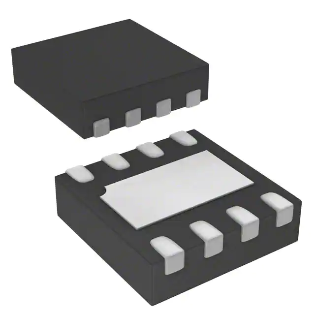


 工商网监
湘ICP备2023018690号
工商网监
湘ICP备2023018690号
