STP04CM05
4-bit constant current power-LED sink driver
Features
■ ■ ■ ■ ■ ■ ■ ■ ■ ■ ■ ■
4 constant current output channels Adjustable output current through one external resistor Can be driven by a 3.3 V microcontroller Serial data IN/parallel data OUT Output current: 80-400 mA 20 V of output driving capability 30 MHz clock frequency UVLO (under voltage lockout) and POR (power ON reset) TSD, thermal shutdown, output off when junction temperature exceeds limit Operating free-air temperature range -40 to 125 ºC ESD protection 2.5 kV HBM, 200 V MM Available in high thermal TSSOP exposed pad. The STP04CM05 guarantees 20 V output driving capability, allowing users to connect more LEDs in series. The high clock frequency, 30 MHz, also satisfies the system requirements which include high volume data transmission. The STP04CM05 is well suited for very high brightness displays and special lighting applications. The STP04CM05 is offered in DIP-14, SO-14 and TSSOP16 exposed pad packages.
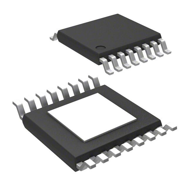
TSSOP16 (Exposed pad) Dip-14 SO-14
Description
The STP04CM05 is a high-power LED driver and 4-bit shift register designed for Power-LED applications. The STP04CM05 contains a 4-bit serial IN, parallel OUT shift register that feeds a 4-bit D-type storage register. In the output stage, four regulated current sources were designed to provide 80-400 mA constant current to drive high power LEDs. Table 1. Device summary
Order codes STP04CM05B1R STP04CM05MTR STP04CM05XTTR Package DIP-14
Packaging 25 parts per tube 2500 parts per reel 2500 parts per reel
SO-14 (tape and reel) TSSOP16 exposed-pad (tape and reel)
June 2008
Rev 4
1/24
www.st.com 24
�Contents
STP04CM05
Contents
1 2 Internal schematic . . . . . . . . . . . . . . . . . . . . . . . . . . . . . . . . . . . . . . . . . . . 3 Pin settings . . . . . . . . . . . . . . . . . . . . . . . . . . . . . . . . . . . . . . . . . . . . . . . . 4
2.1 2.2 Pin connection . . . . . . . . . . . . . . . . . . . . . . . . . . . . . . . . . . . . . . . . . . . . . . 4 Pin description . . . . . . . . . . . . . . . . . . . . . . . . . . . . . . . . . . . . . . . . . . . . . . 4
3
Maximum rating . . . . . . . . . . . . . . . . . . . . . . . . . . . . . . . . . . . . . . . . . . . . . 5
3.1 3.2 Thermal data . . . . . . . . . . . . . . . . . . . . . . . . . . . . . . . . . . . . . . . . . . . . . . . 5 Recommended operating conditions . . . . . . . . . . . . . . . . . . . . . . . . . . . . . 6
4 5 6 7 8 9 10
Electrical characteristics . . . . . . . . . . . . . . . . . . . . . . . . . . . . . . . . . . . . . 7 Equivalent circuit of inputs and outputs . . . . . . . . . . . . . . . . . . . . . . . . . 9 Timing diagrams . . . . . . . . . . . . . . . . . . . . . . . . . . . . . . . . . . . . . . . . . . . 11 Test circuit . . . . . . . . . . . . . . . . . . . . . . . . . . . . . . . . . . . . . . . . . . . . . . . . 14 Typical characteristics . . . . . . . . . . . . . . . . . . . . . . . . . . . . . . . . . . . . . . 15 Package mechanical data . . . . . . . . . . . . . . . . . . . . . . . . . . . . . . . . . . . . 17 Revision history . . . . . . . . . . . . . . . . . . . . . . . . . . . . . . . . . . . . . . . . . . . 23
2/24
�STP04CM05
Internal schematic
1
Internal schematic
Figure 1. Block diagram
3/24
�Pin settings
STP04CM05
2
2.1
Pin settings
Pin connection
Figure 2. Pin connection
DIP-14 / SO-14
TSSOP16 (exposed pad)
Note:
The Exposed-pad is electrically not connected
2.2
Pin description
Table 2. Pin description
TSSOP16 pin N° 1, 2 3 4 5 6 7 8, 9, 12 10 11 13 14 15 16 Symbol GND SDI CLK LE OUT 0 OUT 1 N.C. OUT 2 OUT 3 OE SDO R-EXT VDD Name and function Ground terminal Serial data input terminal Clock input terminal Latch input terminal Output terminal Output terminal Not connected Output terminal Output terminal Output enable input terminal (active low) Serial data out terminal Constant current programming 5 V supply voltage terminal DIP-14 and SO-14 pin N° 1 2 3 4 5 6 7, 8 9 10 11 12 13 14
4/24
�STP04CM05
Maximum rating
3
Maximum rating
Stressing the device above the rating listed in the “absolute maximum ratings” table may cause permanent damage to the device. These are stress ratings only and operation of the device at these or any other conditions above those indicated in the operating sections of this specification is not implied. Exposure to absolute maximum rating conditions for extended periods may affect device reliability. Refer also to the STMicroelectronics SURE Program and other relevant quality documents. Table 3.
Symbol VDD VO IO VI IGND fCLK TOPR TSTG Supply voltage Output voltage Output current Input voltage GND terminal current Clock frequency Operating temperature range Storage temperature range
Absolute maximum ratings
Parameter Value 0 to 7 -0.5 to 20 500 -0.4 to VDD+0.4 2000 50 -40 to +125 -55 to +150 Unit V V mA V mA MHz °C °C
3.1
Thermal data
Table 4.
Symbol
RthJA
Thermal data
Parameter Thermal resistance junction-ambient DIP-14 70 (1) SO-14 105 (2) TSSOP16 37.5 (3) Unit °C/W
1. 1 W of dissipated power, mounted on the board 2. 1 W of dissipated power, mounted on SM PCB1 SGS board 3. Using the PCB Multi-Layer JEDEC Standard test boards
5/24
�Maximum rating
STP04CM05
3.2
Recommended operating conditions
Table 5.
Symbol VDD VO IO IOH IOL VIH VIL
Recommended operating conditions
Parameter Supply voltage Output voltage Output current Output current Output current Input voltage Input voltage VDD = 5 V, IO = 350 mA VDD = 3.3 V, IO = 350 mA LE pulse width CLK pulse width Setup time for DATA Hold time for DATA Setup time for LATCH Hold time for ENABLE Clock frequency Operating temperature range Cascade operation
(1)
Test conditions
Min 3.3
Typ 5.0
Max 5.5 19
Unit V V mA mA mA V V
OUTn VDD = 5 V Serial-OUT Serial-OUT
80
400 +1 -1
0.7VDD -0.3 80 250 8 8.5 8.5 VDD = 3.0 to 3.6 V 8.5 8.5 8.5 50
VDD+0.3 0.3VDD
twEN
OE pulse width
ns 150 4 7.5 7.5 7.5 7.0 7.0 30 -40 +125 ns ns ns ns ns ns MHz °C
twLAT twCLK tSETUP(D) tHOLD(D) tSETUP(L) tHOLD(E) fCLK TOPR
1. If multiple devices are cascaded, it may not be possible achieve the maximum data transfer. Please consider the timing conditions carefully.
6/24
�STP04CM05
Electrical characteristics
4
Electrical characteristics
Table 6. Current accuracy
Current accuracy Output voltage Between bits ≥ 1.4 V Typ. ± 1 % Between ICs ±6% 80 to 400 mA Output current
Table 7.
Symbol VIH VIL IOH VOL VOH IOL1 IOL2 ∆IOL1 ∆IOL2 RSIN(up)
Electrical characteristics (VDD = 3.3 to 5 V, TA = 25°C, unless otherwise specified.)
Parameter Input voltage high level Input voltage low level Output leakage current Output voltage (Serial-OUT) Output voltage (Serial-OUT) Output current VOH = 19 V IOL = 1 mA IOH = -1 mA VO = 0.3 VREXT = 980 Ω VO = 1.2 VREXT = 190 Ω VO = 0.3 VREXT = 980 Ω IO = 80 mA VO = 1.2 VREXT = 190 Ω IO = 400 mA 150 100 REXT = OPEN OUT 0 to 3 = OFF REXT = 980 Ω OUT 0 to 3 = OFF REXT = 190 Ω OUT 0 to 3 = OFF REXT = 980 Ω OUT 0 to 3 = ON Supply current (ON) REXT = 190 Ω OUT 0 to 3 = ON VDD-0.4V 75.2 376 ‘ 80 400 1 1 300 200 1 3.8 14 4.0 14.5 84.8 424 1.5 1.5 600 400 1.5 6 18.5 6.0 19 mA Test conditions Min 0.7 VDD GND Typ Max VDD 0.3 VDD 10 0.4 Unit V V µA V V mA mA % % KΩ KΩ
Output current error between bit (All Output ON) Pull-up resistor
RSIN(down) Pull-down resistor IDD(OFF1) IDD(OFF2) Supply current (OFF) IDD(OFF3) IDD(ON1) IDD(ON2)
7/24
�Electrical characteristics Table 8.
Symbol tPLH1
STP04CM05
Switching characteristics (VDD = 3.3 to 5 V, T = 25 °C, unless otherwise specified.)
Parameter Propagation delay time, CLK-OUTn, LE = H, /OE = L Propagation delay time, LE-OUTn, /OE = L Propagation delay time, /OE-OUTn, LE = H Propagation delay time, CLK-SDO Propagation delay time, CLK-OUTn, LE = H, /OE = L Propagation delay time, LE-OUTn, /OE = L Propagation delay time, /OE-OUTn, LE = H Propagation delay time, CLK-SDO Output rise time 10~90% of voltage waveform Output fall time 90~10% of voltage waveform CLK rise time (1) CLK fall time
(1)
Test conditions VDD = 3.3 V VDD = 5 V VDD = 3.3 V VDD = 5 V VDD = 3.3 V VDD = 5 V VDD = 3.3 V VDD = 5 V RL = 5.0 Ω CL = 10 pF IO = 350 mA Rext = 224 Ω VL = 3.0 V VDD = 3.3 V VDD = 5 V VDD = 3.3 V VDD = 5 V VDD = 3.3 V VDD = 5 V VDD = 3.3 V VDD = 5 V VDD = 3.3 V VDD = 5 V VDD = 3.3 V VDD = 5 V VO = 5.0 V Rext = 224 Ω
Min
Typ 82 45 81 43 147 50 8 6 29 23 33 31 16 12 9 6.5 85 50 6.5 5
Max 130
Unit ns
61 135 ns 62 250 ns 76 12 ns 8 42 ns 32 60 ns 47 22 ns 16 13 ns 9 135 ns 76 9 ns 7 5000 5000 ns ns
tPLH2
tPLH3
tPLH
tPHL1
tPHL2
tPHL3
tPHL
tON
tOFF tr tf
1. In order to achieve high cascade data transfer, please consider tr/tf timings carefully.
8/24
�STP04CM05
Equivalent circuit of inputs and outputs
5
Equivalent circuit of inputs and outputs
Figure 3. OE terminal
Figure 4.
LE terminal
Figure 5.
CLK, SDI terminal
9/24
�Equivalent circuit of inputs and outputs Figure 6. SDO terminal
STP04CM05
10/24
�STP04CM05
Timing diagrams
6
Timing diagrams
Figure 7. Timing diagram
OFF ON OFF ON OFF ON OFF ON
Note: 1 2 3
The latches circuit holds data when the LE terminal is low. When the LE terminal is at a high level, the latch circuit holds the data it passes from the input to the output. When the OE terminal is at a low level, the output terminals OUT0 to OUT3 respond to the data, either ON or OFF. When the OE terminal is at a high level, it switches off all the data on the output terminal.
11/24
�Timing diagrams Figure 8. Clock, serial-in, serial-out
STP04CM05
12/24
�STP04CM05 Figure 9. Clock, serial-in, latch, enable, outputs
Timing diagrams
Figure 10. Outputs
13/24
�Test circuit
STP04CM05
7
Test circuit
Figure 11. DC characteristic
Figure 12. AC characteristic
14/24
�STP04CM05
Typical characteristics
8
Typical characteristics
Figure 13. Output current-REXT resistor Figure 14. Output current vs dropout voltage
1400
Temp. = 25°C Vdd = 5.0V Vdrop = from 0.3V to 1.2V Iset = 50mA; 80mA; 100mA; 150mA; 350mA; 400mA;
1800 1600 1400 Rext (Ohm) 1200 1000 800 600 400 200 0 0 100 200 300 400 500 600 Ouput Currnt (mA)
1200 Vdrop (mV) 1000 800 600 400 200 0 0
Avg @ 3.3V Avg @ 5.0V
Temp. = 25°C Vdd = 3.3V; 5.0V
50 100 150 200 250 300 350 400 450 Iset (mA)
Figure 15. Output current vs ± ∆IOL(%)
1000
Io (mA)
100
10
1 0 0.2 0.4 ∆ IoL % 0.6 0.8
15/24
�Typical characteristics Figure 16. Four power-LED typ. application circuit
STP04CM05
3.3 to 5V 0.3 to 1.4V f = 0 to 100kHz
Note:
VL will be determined by the VF of the LEDs Figure 17. Typical output waveform
Note:
Conditions: TA = 25 C ,VDD = 5 V ,VL = 5 V, Rext = 227 Ω, LED = Lumix LXHL TW01
16/24
�STP04CM05
Package mechanical data
9
Package mechanical data
In order to meet environmental requirements, ST offers these devices in ECOPACK® packages. These packages have a lead-free second level interconnect . The category of second level interconnect is marked on the package and on the inner box label, in compliance with JEDEC Standard JESD97. The maximum ratings related to soldering conditions are also marked on the inner box label. ECOPACK is an ST trademark. ECOPACK specifications are available at: www.st.com
17/24
�Package mechanical data
STP04CM05
Table 9.
Dim.
DIP-14 mechanical data
mm. Min Typ Max Min 0.020 1.65 0.5 0.25 20 8.5 2.54 15.24 7.1 5.1 3.3 1.27 2.54 0.050 0.130 0.100 0.335 0.100 0.600 0.280 0.201 0.055 0.020 0.010 0.787 0.065 inch Typ Max
a1 B b b1 D E e e3 F I L Z
0.51 1.39
Figure 18. Package dimensions
18/24
�STP04CM05
Package mechanical data
Table 10.
Dim.
SO-14 mechanical data
mm. Min Typ Max 1.75 0.1 0.2 1.65 0.35 0.19 0.5 45° (typ.) 8.55 5.8 1.27 7.62 3.8 4.6 0.5 4.0 5.3 1.27 0.68 8° (max.) 0.149 0.181 0.019 8.75 6.2 0.336 0.228 0.050 0.300 0.157 0.208 0.050 0.026 0.344 0.244 0.46 0.25 0.013 0.007 0.019 0.003 Min inch Typ Max 0.068 0.007 0.064 0.018 0.010
A a1 a2 b b1 C c1 D E e e3 F G L M S
Figure 19. Package dimensions
19/24
�Package mechanical data Figure 20. TSSOP16 exposed pad mechanical data
STP04CM05
TSSOP16 EXPOSED PAD MECHANICAL DATA
mm. DIM. MIN. A A1 A2 b c D D1 E E1 E2 e K L 0° 0.45 0.60 0.8 0.19 0.09 4.9 1.7 6.2 4.3 1.5 0.65 8° 0.75 0° 0.018 0.024 6.4 4.4 6.6 4.5 5 1 TYP MAX. 1.2 0.15 1.05 0.30 0.20 5.1 0.031 0.007 0.004 0.193 0.067 0.244 0.169 0.059 0.0256 8° 0.030 0.252 0.173 0.260 0.177 0.197 0.004 0.039 MIN. TYP. MAX. 0.047 0.006 0.041 0.012 0.0089 0.201 inch
7419276A
20/24
�STP04CM05
Package mechanical data
Table 11.
Dim.
Tape and reel SO-14
mm. Min Typ Max 330 12.8 20.2 60 22.4 6.4 9 2.1 3.9 7.9 6.6 9.2 2.3 4.1 8.1 0.252 0.354 0.082 0.153 0.311 13.2 0.504 0.795 2.362 0.882 0.260 0.362 0.090 0.161 0.319 Min inch Typ Max 12.992 0.519
A C D N T Ao Bo Ko Po P
Figure 21. Tape and reel dimensions
21/24
�Package mechanical data
STP04CM05
Table 12.
Dim.
TSSOP16 tape and reel
mm. Min Typ Max 330 12.8 20.2 60 22.4 6.7 5.3 1.6 3.9 7.9 6.9 5.5 1.8 4.1 8.1 0.264 0.209 0.063 0.153 0.311 13.2 0.504 0.795 2.362 0.882 0.272 0.217 0.071 0.161 0.319 Min inch Typ Max 12.992 0.519
A C D N T Ao Bo Ko Po P
Figure 22. Tape and reel dimensions
22/24
�STP04CM05
Revision history
10
Revision history
Table 13.
Date 26-Nov-2007 16-Jan-2008 12-Mar-2008 23-Jun-2008
Document revision history
Revision 1 2 3 4 Initial release Added: Figure 15 on page 15 and Figure 17 on page 16, Updated: Table 8 on page 8. Updated: Figure 8 on page 12. Updated: Table 1 on page 1, Figure 20 on page 20. Changes
23/24
�STP04CM05
Please Read Carefully:
Information in this document is provided solely in connection with ST products. STMicroelectronics NV and its subsidiaries (“ST”) reserve the right to make changes, corrections, modifications or improvements, to this document, and the products and services described herein at any time, without notice. All ST products are sold pursuant to ST’s terms and conditions of sale. Purchasers are solely responsible for the choice, selection and use of the ST products and services described herein, and ST assumes no liability whatsoever relating to the choice, selection or use of the ST products and services described herein. No license, express or implied, by estoppel or otherwise, to any intellectual property rights is granted under this document. If any part of this document refers to any third party products or services it shall not be deemed a license grant by ST for the use of such third party products or services, or any intellectual property contained therein or considered as a warranty covering the use in any manner whatsoever of such third party products or services or any intellectual property contained therein.
UNLESS OTHERWISE SET FORTH IN ST’S TERMS AND CONDITIONS OF SALE ST DISCLAIMS ANY EXPRESS OR IMPLIED WARRANTY WITH RESPECT TO THE USE AND/OR SALE OF ST PRODUCTS INCLUDING WITHOUT LIMITATION IMPLIED WARRANTIES OF MERCHANTABILITY, FITNESS FOR A PARTICULAR PURPOSE (AND THEIR EQUIVALENTS UNDER THE LAWS OF ANY JURISDICTION), OR INFRINGEMENT OF ANY PATENT, COPYRIGHT OR OTHER INTELLECTUAL PROPERTY RIGHT. UNLESS EXPRESSLY APPROVED IN WRITING BY AN AUTHORIZED ST REPRESENTATIVE, ST PRODUCTS ARE NOT RECOMMENDED, AUTHORIZED OR WARRANTED FOR USE IN MILITARY, AIR CRAFT, SPACE, LIFE SAVING, OR LIFE SUSTAINING APPLICATIONS, NOR IN PRODUCTS OR SYSTEMS WHERE FAILURE OR MALFUNCTION MAY RESULT IN PERSONAL INJURY, DEATH, OR SEVERE PROPERTY OR ENVIRONMENTAL DAMAGE. ST PRODUCTS WHICH ARE NOT SPECIFIED AS "AUTOMOTIVE GRADE" MAY ONLY BE USED IN AUTOMOTIVE APPLICATIONS AT USER’S OWN RISK.
Resale of ST products with provisions different from the statements and/or technical features set forth in this document shall immediately void any warranty granted by ST for the ST product or service described herein and shall not create or extend in any manner whatsoever, any liability of ST.
ST and the ST logo are trademarks or registered trademarks of ST in various countries. Information in this document supersedes and replaces all information previously supplied. The ST logo is a registered trademark of STMicroelectronics. All other names are the property of their respective owners.
© 2008 STMicroelectronics - All rights reserved STMicroelectronics group of companies Australia - Belgium - Brazil - Canada - China - Czech Republic - Finland - France - Germany - Hong Kong - India - Israel - Italy - Japan Malaysia - Malta - Morocco - Singapore - Spain - Sweden - Switzerland - United Kingdom - United States of America www.st.com
24/24
�


 工商网监
湘ICP备2023018690号
工商网监
湘ICP备2023018690号
