STP08C596
8-BIT CONSTANT CURRENT LED SINK DRIVER
I
8 CONSTANT CURRENT OUTPUT CHANNELS ADJUSTABLE OUTPUT CURRENT THROUGH EXTERNAL RESISTOR SERIAL DATA IN/PARALLEL DATA OUT SERIAL OUT CHANGE STATE ON THE FALLING EDGES OF CLOCK OUTPUT CURRENT: 15-120 mA 25 MHz CLOCK FREQ. EFFICIENCY PACKAGE
DIP-16 SO-16
I
I I
I I I
DESCRIPTION The STP08C596 is a monolithic, medium-voltage, low current power 8-bit shift register designed for LED panel display. The STP08C596 contains a 8-bit serial-in, parallel-out shift register that feeds a 8-bitD-type storage register. In the output stage, eight regulated current sources were designed to provide 15-120mA constant current to drive the LEDs. Compared with the STPIC6C595, the device provides great flexibility and improved performance in LED panel system design. Table 1: Order Codes
Part Number STP08C596B1 STP08C596M STP08C596MTR STP08C596TTR Temp. Range -40°C to -40°C to -40°C to -40°C to 125°C 125°C 125°C 125°C Package DIP-16 SO-16 (Tube) SO-16 (Tape & Reel) TSSOP16 (Tape & Reel) Comments 25 part per tube 50 parts per tube 1000 parts per reel 2500 parts per reel TSSOP16
Trough an external resistor, users may adjust the STP08C596 output current, controlling in this way the light intensity of LEDs. The STP08C596 guarantees 16V output driving capability, allowing users to connect more LEDs in series. The high clock frequency, 25 MHz, also satisfies the system requirement of high volume data transmission.
May 2005
Rev. 9
1/16
�STP08C596
Table 2: Current Accuracy
Current accuracy Output Voltage Between bits ≥ 0.7V TYP. ± 3% Between ICs ± 10% 15 to 120 mA Output Current
Figure 1: Pin Connection
Table 3: Pin Description
PIN N° 1 2 3 4 5-12 13 14 15 16 Symbol GND SDI CLK /LE OUT 0-7 /OE SDO R-EXT VDD Name and Function Ground Terminal Serial data input terminal Clock input terminal Latch input terminal Output terminal Output enable input terminal (active low) Serial data out terminal Constant Current programming 5V Supply voltage terminal
Table 4: Absolute Maximum Ratings
Symbol VDD VO IO VI IGND fCLK TOPR TSTG Supply Voltage Output Voltage Output Current Input Voltage GND Terminal Current Clock Frequency Operating Temperature Range Storage Temperature Range Parameter Value 0 to 7 -0.5 to 16 120 -0.4 to VDD+0.4 980 25 -40 to +125 -55 to +150 Unit V V mA V mA MHz °C °C
Absolute Maximum Ratings are those values beyond which damage to the device may occur. Functional operation under these condition is not implied.
2/16
�STP08C596
Table 5: Thermal Data
Symbol Rthj-amb Parameter Thermal Resistance Junction-ambient DIP-16 90 SO-16 125 TSSOP16 140 Unit °C/W
Table 6: Recommended Operating Conditions
Symbol VDD VO IO IOH IOL VIH VIL twLAT twCLK twEN tHOLD(D) fCLK Parameter Supply Voltage Output Voltage Output Current Output Current Output Current Input Voltage Input Voltage /LE Pulse Width CLK Pulse Width /OE Pulse Width Hold Time for DATA Clock Frequency Cascade Operation VDD = 3.0 to 3.6V OUTn SERIAL-OUT SERIAL-OUT 0.7VDD -0.3 20 20 400 20 15 15 25 15 Test Conditions Min. 4.5 Typ. 5.0 Max. 5.5 16.0 120 +1 -1 VDD+0.3 0.3VDD Unit V V mA mA mA V V ns ns ns ns ns ns MHz
tSETUP(D) Setup Time for DATA tSETUP(L) Setup Time for LATCH
Table 7: Electrical Characteristics (VDD=5V, T = 25°C, unless otherwise specified.)
Symbol VIH VIL IOH VOL VOH IOL1 IOL2 ∆IOL1 ∆IOL2 RSIN(up) Output Current Error between bit (All Output ON) Pull-up Resistor REXT = OPEN REXT = 470 Ω REXT = 250 Ω Supply Current (ON) REXT = 470 Ω REXT = 250 Ω OUT 0 to 7 = OFF OUT 0 to 7 = OFF OUT 0 to 7 = OFF OUT 0 to 7 = ON OUT 0 to 7 = ON Parameter Input Voltage High Level Input Voltage Low Level Output Leakage Current VOH = 16 V VDD-0.4V 20.6 50.6 20.7 51.0 20.9 51.5 ±3 ±3 150 100 300 200 0.3 5.5 10.1 5.5 10.1 600 400 0.6 7.7 14.1 7.7 14.1 Output Voltage (Serial-OUT) IOL = 1mA Output Voltage (Serial-OUT) IOH = -1mA Output Current VO = 0.7V REXT = 910 Ω VO = 0.7V REXT = 360 Ω VO = 0.7V REXT = 910 Ω VO = 0.7V REXT = 360 Ω Test Conditions Min. 0.7VDD GND Typ. Max. VDD 0.3VDD 10 0.4 Unit V V µA V V mA mA % % KΩ KΩ mA
RSIN(down) Pull-down Resistor IDD(OFF1) Supply Current (OFF) IDD(OFF2) IDD(OFF3) IDD(ON1) IDD(ON2)
3/16
�STP08C596
Table 8: Switching Characteristics (VDD=5V, T = 25°C, unless otherwise specified.)
Symbol tPLH1 tPLH2 tPLH3 tPLH tPHL1 tPHL2 tPHL3 tPHL tr tf Parameter Propagation Delay Time, CLK-OUTn, /LE = H, /OE = L Propagation Delay Time, /LE-OUTn, /OE = L Propagation Delay Time, /OE-OUTn, /LE = H Propagation Delay Time, CLK-SDO Propagation Delay Time, CLK-OUTn, /LE = H, /OE = L Propagation Delay Time, /LE-OUTn, /OE = L Propagation Delay Time, /OE-OUTn, /LE = H Propagation Delay Time, CLK-SDO Output Rise Time Output Fall Time Test Conditions VDD = 5 V VIL = GND IO = 40mA REXT = 470 Ω VIH = VDD CL = 13pF VL = 3 V RL = 65 Ω 145 15 15 15 45 15 160 15 200 30 30 30 60 300 200 25 ns ns ns ns ns ns ns ns Min. Typ. 200 160 Max. 280 250 Unit ns ns
EQUIVALENT CIRCUIT OF INPUTS AND OUTPUTS Figure 2: /OE Terminal
4/16
�STP08C596
Figure 3: /LE Terminal
Figure 4: CLK, SDI Terminal
Figure 5: SDO Terminal
5/16
�STP08C596
Figure 6: Block Diagram
Figure 7: Timing Diagram
6/16
�STP08C596
Figure 8: Clock, Serial-In, Serial-Out
Figure 9: Clock, Serial-In, Latch, Enable, Outputs
7/16
�STP08C596
Figure 10: Outputs
TEST CIRCUIT Figure 11: DC Characteristic
8/16
�STP08C596
Figure 12: AC Characteristic
Figure 13: Output Current-R EXT Resistor
Figure 14: Power Dissipation vs Temperature Package
9/16
�STP08C596
Plastic DIP-16 (0.25) MECHANICAL DATA
mm. DIM. MIN. a1 B b b1 D E e e3 F I L Z 3.3 1.27 8.5 2.54 17.78 7.1 5.1 0.130 0.050 0.51 0.77 0.5 0.25 20 0.335 0.100 0.700 0.280 0.201 1.65 TYP MAX. MIN. 0.020 0.030 0.020 0.010 0.787 0.065 TYP. MAX. inch
P001C
10/16
�STP08C596
SO-16 MECHANICAL DATA
DIM. A a1 a2 b b1 C c1 D E e e3 F G L M S 3.8 4.6 0.5 9.8 5.8 1.27 8.89 4.0 5.3 1.27 0.62 8° (max.) 0.149 0.181 0.019 10 6.2 0.35 0.19 0.5 45° (typ.) 0.385 0.228 0.050 0.350 0.157 0.208 0.050 0.024 0.393 0.244 0.1 mm. MIN. TYP MAX. 1.75 0.25 1.64 0.46 0.25 0.013 0.007 0.019 0.004 MIN. inch TYP. MAX. 0.068 0.010 0.063 0.018 0.010
0016020D
11/16
�STP08C596
TSSOP16 MECHANICAL DATA
mm. DIM. MIN. A A1 A2 b c D E E1 e K L 0˚ 0.45 0.60 0.05 0.8 0.19 0.09 4.9 6.2 4.3 5 6.4 4.4 0.65 BSC 8˚ 0.75 0˚ 0.018 0.024 1 TYP MAX. 1.2 0.15 1.05 0.30 0.20 5.1 6.6 4.48 0.002 0.031 0.007 0.004 0.193 0.244 0.169 0.197 0.252 0.173 0.0256 BSC 8˚ 0.030 0.004 0.039 MIN. TYP. MAX. 0.047 0.006 0.041 0.012 0.0079 0.201 0.260 0.176 inch
A
A2 A1 b e K c L E
D
E1
PIN 1 IDENTIFICATION
1
0080338D
12/16
�STP08C596
Tape & Reel SO-16 MECHANICAL DATA
mm. DIM. MIN. A C D N T Ao Bo Ko Po P 6.45 10.3 2.1 3.9 7.9 12.8 20.2 60 22.4 6.65 10.5 2.3 4.1 8.1 0.254 0.406 0.082 0.153 0.311 TYP MAX. 330 13.2 0.504 0.795 2.362 0.882 0.262 0.414 0.090 0.161 0.319 MIN. TYP. MAX. 12.992 0.519 inch
13/16
�STP08C596
Tape & Reel TSSOP16 MECHANICAL DATA
mm. DIM. MIN. A C D N T Ao Bo Ko Po P 6.7 5.3 1.6 3.9 7.9 12.8 20.2 60 22.4 6.9 5.5 1.8 4.1 8.1 0.264 0.209 0.063 0.153 0.311 TYP MAX. 330 13.2 0.504 0.795 2.362 0.882 0.272 0.217 0.071 0.161 0.319 MIN. TYP. MAX. 12.992 0.519 inch
14/16
�STP08C596
Table 9: Revision History
Date 03-Aug-2004 23-Feb-2005 31-Mar-2005 02-May-2005 Revision 6 7 8 9 Description of Changes Package TSSOP (Exposed Pad) removed. Table 8 - pag. 4 data changed. Figure 14 - pag. 10 changed. Mistake on Table 7 - IDDOFF and IDDON OUT 0 to 15 ==> OUT 0 to 7. Mistake on Fig. 7. Typing Error on the description features.
15/16
�STP08C596
Information furnished is believed to be accurate and reliable. However, STMicroelectronics assumes no responsibility for the consequences of use of such information nor for any infringement of patents or other rights of third parties which may result from its use. No license is granted by implication or otherwise under any patent or patent rights of STMicroelectronics. Specifications mentioned in this publication are subject to change without notice. This publication supersedes and replaces all information previously supplied. STMicroelectronics products are not authorized for use as critical components in life support devices or systems without express written approval of STMicroelectronics. The ST logo is a registered trademark of STMicroelectronics All other names are the property of their respective owners © 2005 STMicroelectronics - All Rights Reserved STMicroelectronics group of companies Australia - Belgium - Brazil - Canada - China - Czech Republic - Finland - France - Germany - Hong Kong - India - Israel - Italy - Japan Malaysia - Malta - Morocco - Singapore - Spain - Sweden - Switzerland - United Kingdom - United States of America www.st.com
16/16
�
很抱歉,暂时无法提供与“STP08C596MTR”相匹配的价格&库存,您可以联系我们找货
免费人工找货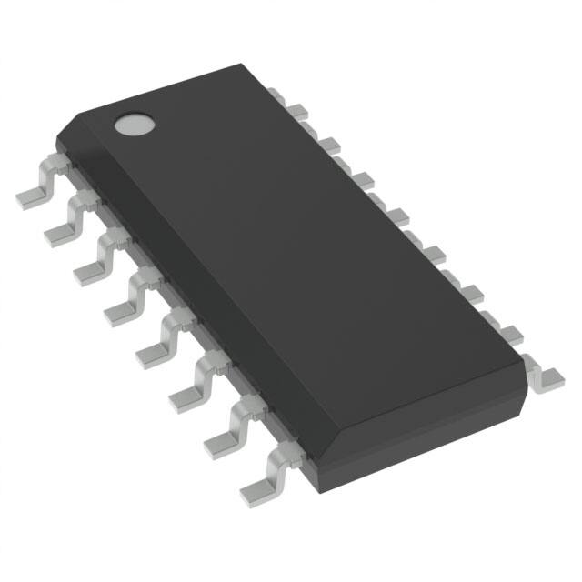


 工商网监
湘ICP备2023018690号
工商网监
湘ICP备2023018690号
