STW29NK50ZD
N-CHANNEL 500 V - 0.095Ω - 29A TO-247
Fast Diode SuperMESH™ MOSFET
Table 1: General Features
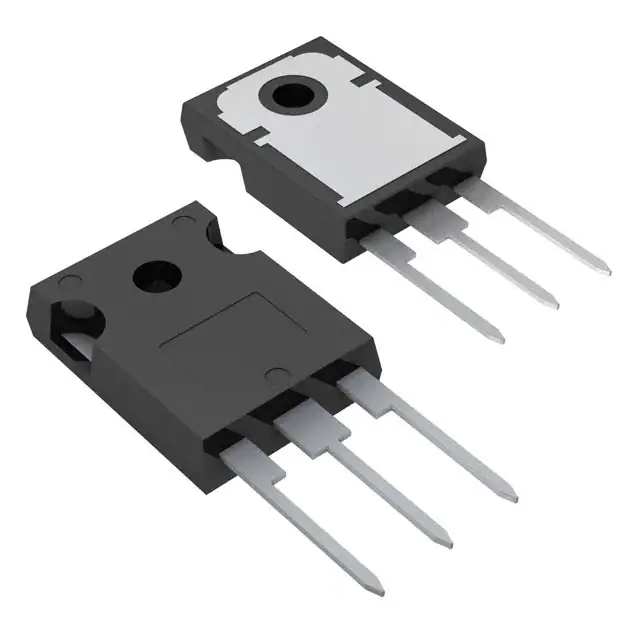
Figure 1: Package
TYPE
VDSS
RDS(on)
ID
PW
STW29NK50ZD
500 V
< 0.13 Ω
29 A
350 W
)
s
(
t
c
u
d
o s)
r
(
P
t
c
e u
t
e
l od
o
s Pr
b
O ete
l
)
o
s
(
s
t
b
c
u -O
d
o s)
r
P
(
t
e uc
t
e
l od
o
s Pr
b
O te
e
l
o
s
b
■
■
■
■
■
■
■
TYPICAL RDS(on) = 0.095 Ω
HIGH dv/dt CAPABILITY
100% AVALANCHE TESTED
GATE CHARGE MINIMIZED
LOW INTRINSIC CAPACITANCES
VERY GOOD MANUFACTURING
REPEATIBILITY
FAST INTERNAL RECOVERY TIME
DESCRIPTION
The Fast SuperMesh™ series associates all advantages of reduced on-resistance, zener gate
protection and very goog dv/dt capability with a
Fast body-drain recovery diode. Such series complements the “FDmesh™” Advanced Technology.
3
2
1
TO-247
Figure 2: Internal Schematic Diagram
APPLICATIONS
■ HID BALLAST
■ ZVS PHASE-SHIFT FULL BRIDGE
Table 2: Order Codes
O
PART NUMBER
MARKING
PACKAGE
PACKAGING
STW29NK50ZD
W29NK50ZD
TO-247
TUBE
Rev. 3
July 2005
1/10
�STW29NK50ZD
Table 3: Absolute Maximum ratings
Symbol
VDS
VDGR
VGS
Parameter
Drain-source Voltage (VGS = 0)
Value
Unit
500
V
Drain-gate Voltage (RGS = 20 KΩ)
500
V
Gate- source Voltage
± 30
V
ID
Drain Current (continuous) at TC = 25°C
29
A
ID
Drain Current (continuous) at TC = 100°C
18.27
A
IDM(*)
Drain Current (pulsed)
116
A
PTOT
Total Dissipation at TC = 25°C
350
W
)
s
(
t
c
u
d
o s)
r
(
P
t
c
e u
t
e
l od
o
s Pr
b
O ete
l
)
o
s
(
s
t
b
c
u -O
d
o s)
r
P
(
t
e uc
t
e
l od
o
s Pr
b
O te
e
l
o
s
b
VESD(G-S)
dv/dt (1)
Tstg
Tj
Derating Factor
2.77
Gate source ESD (HBM-C = 100pF, R = 1.5 KΩ)
6000
V
4.5
V/ns
-55 to 150
°C
Peak Diode Recovery voltage slope
Storage Temperature
Operating Junction Temperature
W/°C
(*) Pulse width limited by safe operating area
(1) ISD≤ 29 A, di/dt≤ 200 A/µs, VDD≤ 400V
Table 4: Thermal Data
Rthj-case
Thermal Resistance Junction-case Max
0.36
°C/W
Rthj-amb
Tl
Thermal Resistance Junction-ambient Max
Maximum Lead Temperature For Soldering Purpose
50
300
°C/W
°C
Max Value
Unit
Table 5: Avalanche Characteristics
Symbol
Parameter
IAR
Avalanche Current, Repetitive or Not-Repetitive
(pulse width limited by Tj max)
29
A
EAS
Single Pulse Avalanche Energy
(starting Tj = 25 °C, ID = IAR, VDD = 50 V)
500
mJ
Table 6: Gate-Source Zener Diode
Symbol
BVGSO
Parameter
Gate-Source Breakdown
Voltage
Test Condition
Min.
Igs= ± 1mA (Open Drain)
30
Typ.
Max
Unit
A
PROTECTION FEATURES OF GATE-TO-SOURCE ZENER DIODES
The built-in back-to-back Zener diodes have specifically been designed to enhance not only the device’s
ESD capability, but also to make them safely absorb possible voltage transients that may occasionally be
applied from gate to source. In this respect the Zener voltage is appropriate to achieve an efficient and
cost-effective intervention to protect the device’s integrity. These integrated Zener diodes thus avoid the
usage of external components.
O
2/10
�STW29NK50ZD
TABLE 7: ELECTRICAL CHARACTERISTICS (TCASE =25°C UNLESS OTHERWISE SPECIFIED)
On /Off
Symbol
Parameter
Test Conditions
V(BR)DSS
Drain-source Breakdown
Voltage
ID = 1 mA, VGS = 0
IDSS
Zero Gate Voltage
Drain Current (VGS = 0)
VDS = Max Rating
VDS = Max Rating, TC = 125°C
IGSS
Gate-body Leakage
Current (VDS = 0)
VGS = ± 20 V
VGS(th)
Gate Threshold Voltage
VDS = VGS, ID = 150 µA
RDS(on
Static Drain-source On
Resistance
VGS = 10 V, ID = 14.5 A
Min.
Typ.
Max.
500
3
Unit
S
1
50
µA
µA
± 10
µA
3.75
4.5
V
0.095
0.13
Ω
Typ.
Max.
Unit
)
s
(
t
c
u
d
o s)
r
(
P
t
c
e u
t
e
l od
o
s Pr
b
O ete
l
)
o
s
(
s
t
b
c
u -O
d
o s)
r
P
(
t
e uc
t
e
l od
o
s Pr
b
O te
e
l
o
s
b
Table 8: Dynamic
Symbol
gfs (1)
Parameter
Test Conditions
Forward Transconductance
VDS = 15 V, ID = 14.5 A
Ciss
Coss
Crss
Input Capacitance
Output Capacitance
Reverse Transfer
Capacitance
td(on)
tr
td(off)
tf
Qg
Qgs
Qgd
Min.
28
S
VDS = 25 V, f = 1 MHz, VGS = 0
6450
710
165
pF
pF
pF
Turn-on Delay Time
Rise Time
Turn-off-Delay Time
Fall Time
VDD = 400 V, ID = 14.5 A,
RG = 4.7 Ω, VGS = 10 V
(d see Figure 17)
45
43
133
25
ns
ns
ns
ns
Total Gate Charge
Gate-Source Charge
Gate-Drain Charge
VDD = 480 V, ID = 14.5 A,
VGS = 10 V
180
33
108
200
nC
nC
nC
Typ.
Max.
Unit
29
116
A
A
1.6
V
Table 9: Source Drain Diode
Symbol
Parameter
ISD
ISDM (2)
Source-drain Current
Source-drain Current (pulsed)
VSD (1)
Forward On Voltage
ISD = 29 A, VGS = 0
Reverse Recovery Time
Reverse Recovery Charge
Reverse Recovery Current
ISD = 29 A, di/dt = 100 A/µs
VDD = 30V, Tj = 25°C
(see Figure 18)
264
2.08
15.7
ns
µC
A
Reverse Recovery Time
Reverse Recovery Charge
Reverse Recovery Current
ISD = 29 A, di/dt = 100 A/µs
VDD = 30V, Tj = 150°C
(see Figure 18)
395
4.164
21.1
ns
µC
A
trr
Qrr
IRRM
trr
Qrr
IRRM
Test Conditions
Min.
O
(1) Pulsed: Pulse duration = 300 µs, duty cycle 1.5 %.
(2) Pulse width limited by safe operating area.
3/10
�STW29NK50ZD
Figure 3: Safe Operating Area
Figure 6: Thermal Impedance
)
s
(
t
c
u
d
o s)
r
(
P
t
c
e u
t
e
l od
o
s Pr
b
O ete
l
)
o
s
(
s
t
b
c
u -O
d
o s)
r
P
(
t
e uc
t
e
l od
o
s Pr
b
O te
e
l
o
s
b
Figure 4: Output Characteristics
Figure 7: Transfer Characteristics
Figure 5: Transconductance
Figure 8: Static Drain-source On Resistance
O
4/10
�STW29NK50ZD
Figure 9: Gate Charge vs Gate-source Voltage
Figure 12: Capacitance Variations
)
s
(
t
c
u
d
o s)
r
(
P
t
c
e u
t
e
l od
o
s Pr
b
O ete
l
)
o
s
(
s
t
b
c
u -O
d
o s)
r
P
(
t
e uc
t
e
l od
o
s Pr
b
O te
e
l
o
s
b
Figure 10: Normalized Gate Thereshold Voltage vs Temperature
Figure 13: Normalized On Resistance vs Temperature
Figure 11: Source-Drain Diode Forward Characteristics
Figure 14: Normalized BVdss vs Temperature
O
5/10
�STW29NK50ZD
Figure 15: Avalanche Energy vs Starting Tj
)
s
(
t
c
u
d
o s)
r
(
P
t
c
e u
t
e
l od
o
s Pr
b
O ete
l
)
o
s
(
s
t
b
c
u -O
d
o s)
r
P
(
t
e uc
t
e
l od
o
s Pr
b
O te
e
l
o
s
b
O
6/10
�STW29NK50ZD
Figure 16: Unclamped Inductive Load Test Circuit
Figure 19: Unclamped Inductive Wafeform
)
s
(
t
c
u
d
o s)
r
(
P
t
c
e u
t
e
l od
o
s Pr
b
O ete
l
)
o
s
(
s
t
b
c
u -O
d
o s)
r
P
(
t
e uc
t
e
l od
o
s Pr
b
O te
e
l
o
s
b
Figure 17: Switching Times Test Circuit For
Resistive Load
Figure 20: Gate Charge Test Circuit
Figure 18: Test Circuit For Inductive Load
Switching and Diode Recovery Times
O
7/10
�STW29NK50ZD
TO-247 MECHANICAL DATA
DIM.
mm.
MIN.
TYP
inch
MAX.
MIN.
TYP.
MAX.
A
4.85
5.15
0.19
0.20
A1
2.20
2.60
0.086
0.102
b
1.0
1.40
0.039
0.055
b1
2.0
2.40
0.079
0.094
)
s
(
t
c
u
d
o s)
r
(
P
t
c
e u
t
e
l od
o
s Pr
b
O ete
l
)
o
s
(
s
t
b
c
u -O
d
o s)
r
P
(
t
e uc
t
e
l od
o
s Pr
b
O te
e
l
o
s
b
b2
3.0
3.40
0.118
0.134
c
0.40
0.80
0.015
0.03
D
19.85
20.15
0.781
0.793
E
15.45
15.75
0.608
0.620
14.80
0.560
4.30
0.14
e
5.45
L
14.20
L1
3.70
L2
O
8/10
18.50
øP
3.55
øR
4.50
S
0.214
5.50
0.582
0.17
0.728
3.65
0.140
5.50
0.177
0.143
0.216
0.216
�STW29NK50ZD
Table 10: Revision History
Date
Revision
05-Feb-2004
06-Dec-2004
20-Jul-2005
1
2
3
Description of Changes
First Release.
Some electrical value changed
Complete version
)
s
(
t
c
u
d
o s)
r
(
P
t
c
e u
t
e
l od
o
s Pr
b
O ete
l
)
o
s
(
s
t
b
c
u -O
d
o s)
r
P
(
t
e uc
t
e
l od
o
s Pr
b
O te
e
l
o
s
b
O
9/10
�STW29NK50ZD
)
s
(
t
c
u
d
o s)
r
(
P
t
c
e u
t
e
l od
o
s Pr
b
O ete
l
)
o
s
(
s
t
b
c
u -O
d
o s)
r
P
(
t
e uc
t
e
l od
o
s Pr
b
O te
e
l
o
s
b
Information furnished is believed to be accurate and reliable. However, STMicroelectronics assumes no responsibility for the consequences
of use of such information nor for any infringement of patents or other rights of third parties which may result from its use. No license is granted
by implication or otherwise under any patent or patent rights of STMicroelectronics. Specifications mentioned in this publication are subject
to change without notice. This publication supersedes and replaces all information previously supplied. STMicroelectronics products are not
authorized for use as critical components in life support devices or systems without express written approval of STMicroelectronics.
O
The ST logo is a registered trademark of STMicroelectronics
All other names are the property of their respective owners
© 2005 STMicroelectronics - All Rights Reserved
STMicroelectronics group of companies
Australia - Belgium - Brazil - Canada - China - Czech Republic - Finland - France - Germany - Hong Kong - India - Israel - Italy - Japan Malaysia - Malta - Morocco - Singapore - Spain - Sweden - Switzerland - United Kingdom - United States of America
www.st.com
10/10
�
很抱歉,暂时无法提供与“STW29NK50ZD”相匹配的价格&库存,您可以联系我们找货
免费人工找货