®
VN920SP
SINGLE CHANNEL HIGH SIDE SOLID STATE RELAY
TYPE VN920SP
s
RDS(on) 15mΩ
IOUT 30 A
VCC 36 V
CMOS COMPATIBLE INPUT s PROPORTIONAL LOAD CURRENT SENSE s SHORTED LOAD PROTECTION s UNDERVOLTAGE AND OVERVOLTAGE SHUTDOWN s OVERVOLTAGE CLAMP s THERMAL SHUTDOWN s CURRENT LIMITATION PROTECTION AGAINST LOSS OF GROUND AND LOSS VCC s VERY LOW STAND-BY POWER DISSIPATION s REVERSE BATTERY PROTECTION (*)
s
10
1
PowerSO-10™
ORDER CODES
PACKAGE TUBE T&R VN920SP13TR
PowerSO-10™ VN920SP
DESCRIPTION The VN920SP is a monolithic device designed in STMicroelectronics VIPower M0-3 Technology, intended for driving any kind of load with one side connected to ground. Active VCC pin voltage clamp protects the device against low energy BLOCK DIAGRAM
spikes (see ISO7637 transient compatibility table). Active current limitation combined with thermal shutdown and automatic restart protect the device against overload. The device integrates an analog current sense output which delivers a current proportional to the load current. Device automatically turns off in case of ground pin disconnection.
VCC
VCC CLAMP
OVERVOLTAGE DETECTION UNDERVOLTAGE DETECTION
GND
Power CLAMP
DRIVER INPUT LOGIC CURRENT LIMITER VDS LIMITER IOUT K OVERTEMPERATURE DETECTION CURRENT SENSE OUTPUT
(*) See application schematic at page 8
October 2002
1/16
1
�VN920SP
ABSOLUTE MAXIMUM RATING
Symbol VCC - VCC - IGND IOUT - IOUT IIN VCSENSE Parameter DC Supply Voltage Reverse DC Supply Voltage DC Reverse Ground Pin Current DC Output Current Reverse DC Output Current DC Input Current Current Sense Maximum Voltage Electrostatic Discharge (Human Body Model: R=1.5KΩ; C=100pF) VESD - INPUT - CURRENT SENSE - OUTPUT - VCC Maximum Switching Energy (L=0.25mH; RL=0Ω; Vbat=13.5V; Tjstart=150ºC; IL=45A) Power Dissipation TC≤25°C Junction Operating Temperature Case Operating Temperature Storage Temperature 4000 2000 5000 5000 362 96.1 Internally limited - 40 to 150 - 55 to 150 V V V V mJ W °C °C °C Value 41 - 0.3 - 200 Internally Limited - 40 +/- 10 -3 +15 Unit V V mA A A mA V V
EMAX Ptot Tj Tc TSTG
CONNECTION DIAGRAM (TOP VIEW)
GROUND INPUT C.SENSE N.C. N.C.
6 7 8 9 10 11 VCC
5 4 3 2 1
OUTPUT OUTPUT N.C. OUTPUT OUTPUT
CURRENT AND VOLTAGE CONVENTIONS
IS VCC VCC IOUT OUTPUT IIN INPUT VIN CURRENT SENSE VSENSE GND IGND ISENSE VOUT
2/16
1
�VN920SP
THERMAL DATA
Symbol Rthj-case Rthj-amb Parameter Thermal Resistance Junction-case Thermal Resistance Junction-ambient
Max Max
Value 1.3 51.3 (*)
Unit °C/W °C/W
(*) When mounted on a standard single-sided FR-4 board with 0.5cm2 of Cu (at least 35µm thick).
ELECTRICAL CHARACTERISTICS (8V
很抱歉,暂时无法提供与“VN920SP”相匹配的价格&库存,您可以联系我们找货
免费人工找货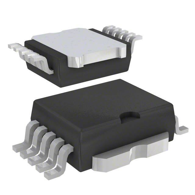


 工商网监
湘ICP备2023018690号
工商网监
湘ICP备2023018690号
