VNQ7004SY
Quad-channel high-side driver with 16-bit SPI interface for
automotive applications
Datasheet - production data
– Undervoltage shutdown
– Overvoltage clamp
– Latch-off or programmable time limited
auto restart (power limitation and
overtemperature shutdown)
– Load dump protected
– Protection against loss of ground
Features
Description
Channel
VCC
RON(typ)
ILIMH(typ)
0–1
28 V
35 mΩ
35 A
2–3
28 V
9 mΩ
80 A
AEC-Q100 qualified
General
– 16-bit ST-SPI for full diagnostic with 8 bits
Short Frame option
– Programmable Bulb/LED mode for
ch. 0-1
– Advanced limp home functions for robust
fail-safe system
– Very low standby current
– Optimized electromagnetic emissions
– Very low electromagnetic susceptibility
– Control through direct inputs and / or SPI
– Compliant with European directive
2002/95/EC
Diagnostic functions
– Multiplex proportional load current sense
– Synchronous diagnostic of over load and
short to GND, output shorted to VCC and
OFF-state open-load
– Programmable case overtemperature
warning
Protection
– Two levels load current limitation
– Self limiting of fast thermal transients
December 2018
This is information on a product in full production.
The VNQ7004SY is a device made using
STMicroelectronics® VIPower® technology. It is
intended for driving resistive or inductive loads
directly connected to ground. The device is
protected against voltage transient on VCC pin.
An 8 bit short frame access to output control
registers is provided allowing PWM control
through SPI with high granularity.
An analog current feedback for each channel is
connected to the CURRENT-SENSE pin via a
multiplexer. The device detects open-load in OFFstate conditions.
Real time diagnostic is available through the SPI
bus (open-load, output short to VCC,
overtemperature, communication error, power
limitation or latch off).
Output current limitation protects the device in an
over load condition. The device can limit the
dissipated power to a safe level up to thermal
shutdown intervention. Thermal shutdown can be
configured as latched off or programmable time
limited auto restart.
The device enters a limp home mode in case of
loss of digital supply (VDD), reset of digital
memory or watchdog monitoring time-out event.
In this mode states of channel 0, 1, 2 or 3 are
respectively controlled by four dedicated pins IN0,
IN1, IN2 and IN3. Channel 0 and 1 can be
programmed via SPI for load type (BULB/ LED
mode).
DS12442 Rev 3
1/95
www.st.com
�Contents
VNQ7004SY
Contents
1
Block diagram and pin description . . . . . . . . . . . . . . . . . . . . . . . . . . . . . 8
2
Functional description . . . . . . . . . . . . . . . . . . . . . . . . . . . . . . . . . . . . . . 11
3
4
2.1
Device interfaces . . . . . . . . . . . . . . . . . . . . . . . . . . . . . . . . . . . . . . . . . . . .11
2.2
Operating modes . . . . . . . . . . . . . . . . . . . . . . . . . . . . . . . . . . . . . . . . . . . .11
Startup transition phase . . . . . . . . . . . . . . . . . . . . . . . . . . . . . . . . . . . . . 11
2.2.2
Reset mode . . . . . . . . . . . . . . . . . . . . . . . . . . . . . . . . . . . . . . . . . . . . . . 11
2.2.3
Fail Safe mode . . . . . . . . . . . . . . . . . . . . . . . . . . . . . . . . . . . . . . . . . . . . 12
2.2.4
Normal mode . . . . . . . . . . . . . . . . . . . . . . . . . . . . . . . . . . . . . . . . . . . . . 13
2.2.5
Standby mode . . . . . . . . . . . . . . . . . . . . . . . . . . . . . . . . . . . . . . . . . . . . 15
2.2.6
Sleep mode 1 . . . . . . . . . . . . . . . . . . . . . . . . . . . . . . . . . . . . . . . . . . . . . 17
2.2.7
Sleep mode 2 . . . . . . . . . . . . . . . . . . . . . . . . . . . . . . . . . . . . . . . . . . . . . 17
2.2.8
Battery undervoltage mode . . . . . . . . . . . . . . . . . . . . . . . . . . . . . . . . . . 17
2.2.9
Limp Home mode . . . . . . . . . . . . . . . . . . . . . . . . . . . . . . . . . . . . . . . . . 19
Protections . . . . . . . . . . . . . . . . . . . . . . . . . . . . . . . . . . . . . . . . . . . . . . . . 23
3.1
Pre-warning . . . . . . . . . . . . . . . . . . . . . . . . . . . . . . . . . . . . . . . . . . . . . . . 23
3.2
Junction overtemperature (OT) . . . . . . . . . . . . . . . . . . . . . . . . . . . . . . . . 23
3.3
Power limitation (PL) . . . . . . . . . . . . . . . . . . . . . . . . . . . . . . . . . . . . . . . . 24
SPI functional description . . . . . . . . . . . . . . . . . . . . . . . . . . . . . . . . . . . 26
4.1
4.2
4.3
2/95
2.2.1
SPI communication . . . . . . . . . . . . . . . . . . . . . . . . . . . . . . . . . . . . . . . . . 26
4.1.1
Signal description . . . . . . . . . . . . . . . . . . . . . . . . . . . . . . . . . . . . . . . . . 26
4.1.2
Connecting to the SPI bus . . . . . . . . . . . . . . . . . . . . . . . . . . . . . . . . . . . 27
4.1.3
SPI mode . . . . . . . . . . . . . . . . . . . . . . . . . . . . . . . . . . . . . . . . . . . . . . . . 27
SPI protocol . . . . . . . . . . . . . . . . . . . . . . . . . . . . . . . . . . . . . . . . . . . . . . . 28
4.2.1
SDI format . . . . . . . . . . . . . . . . . . . . . . . . . . . . . . . . . . . . . . . . . . . . . . . 28
4.2.2
SDO format . . . . . . . . . . . . . . . . . . . . . . . . . . . . . . . . . . . . . . . . . . . . . . 29
4.2.3
Operating code definition . . . . . . . . . . . . . . . . . . . . . . . . . . . . . . . . . . . . 29
4.2.4
Special commands . . . . . . . . . . . . . . . . . . . . . . . . . . . . . . . . . . . . . . . . . 32
Register map . . . . . . . . . . . . . . . . . . . . . . . . . . . . . . . . . . . . . . . . . . . . . . 33
4.3.1
Global Status byte description . . . . . . . . . . . . . . . . . . . . . . . . . . . . . . . . 33
4.3.2
RAM . . . . . . . . . . . . . . . . . . . . . . . . . . . . . . . . . . . . . . . . . . . . . . . . . . . . 34
4.3.3
ROM . . . . . . . . . . . . . . . . . . . . . . . . . . . . . . . . . . . . . . . . . . . . . . . . . . . 35
DS12442 Rev 3
�VNQ7004SY
Contents
4.3.4
5
4.4
Output switching slopes control . . . . . . . . . . . . . . . . . . . . . . . . . . . . . . . . 38
4.5
Output control . . . . . . . . . . . . . . . . . . . . . . . . . . . . . . . . . . . . . . . . . . . . . . 38
4.6
Control registers . . . . . . . . . . . . . . . . . . . . . . . . . . . . . . . . . . . . . . . . . . . . 40
4.6.1
Address 0x00h — Control Register (CTLR) . . . . . . . . . . . . . . . . . . . . . 40
4.6.2
Address 0x01h — Direct Input Enable Control Register (DIENCR) . . . 41
4.6.3
Address 0x02h — Open-load OFF-State Control Register (OLOFFCR) 42
4.6.4
Address 0x03h — Channel Control Register (CCR) . . . . . . . . . . . . . . . 42
4.6.5
Address 0x04h — Fast Switching Configuration Register (FASTSWCR)
. . . . . . . . . . . . . . . . . . . . . . . . . . . . . . . . . . . . . . . . . . . . . . . . . . . . . . . . 42
4.6.6
Address 0x06h — CurrentSense Multiplexer Control Register
(CSMUXCR) . . . . . . . . . . . . . . . . . . . . . . . . . . . . . . . . . . . . . . . . . . . . . 43
4.6.7
Address 0x07h — SPI Output Control Register (SOCR) . . . . . . . . . . . . 43
4.6.8
Address 0x08h — Channel Latch OFF Timer Control Register (ch0, ch1)
(CHLOFFTCR0,1) . . . . . . . . . . . . . . . . . . . . . . . . . . . . . . . . . . . . . . . . . 44
4.6.9
Address 0x09h — Channel Latch OFF Timer Control Register (ch2, ch3)
(CHLOFFTCR2,3) . . . . . . . . . . . . . . . . . . . . . . . . . . . . . . . . . . . . . . . . . 44
Diagnostic . . . . . . . . . . . . . . . . . . . . . . . . . . . . . . . . . . . . . . . . . . . . . . . . 46
5.1
Analogue diagnostic . . . . . . . . . . . . . . . . . . . . . . . . . . . . . . . . . . . . . . . . . 46
5.2
Digital diagnostic . . . . . . . . . . . . . . . . . . . . . . . . . . . . . . . . . . . . . . . . . . . 46
5.2.1
6
SPI modes . . . . . . . . . . . . . . . . . . . . . . . . . . . . . . . . . . . . . . . . . . . . . . . 36
Status registers . . . . . . . . . . . . . . . . . . . . . . . . . . . . . . . . . . . . . . . . . . . 48
5.3
Over load (VDS high voltage, Over Load (OVL)) . . . . . . . . . . . . . . . . . . . 48
5.4
Open-load ON-state detection . . . . . . . . . . . . . . . . . . . . . . . . . . . . . . . . . 49
5.5
Open-load OFF-state detection . . . . . . . . . . . . . . . . . . . . . . . . . . . . . . . . 49
5.6
Address 0x2Fh — DIENSR: Direct Input Status register . . . . . . . . . . . . . 50
5.7
Address 0x30h — Channel Feedback Status Register (CHFBSR) . . . . . 51
5.8
Address 0x31h — Open-load OFF-State / Stuck to VCC Status Register
(OLOFFCR) . . . . . . . . . . . . . . . . . . . . . . . . . . . . . . . . . . . . . . . . . . . . . . . 51
5.9
Address 0x32h — Channels latch-off status register (CHLOFFSR) . . . . 52
5.10
Address 0x33h — VDS Feedback Status Register (VDSFSR) . . . . . . . . 52
5.11
Address 0x34h — Generic Status Register (GENSR) . . . . . . . . . . . . . . . 53
5.12
Address 0x3Fh — Configuration Register (CONFIG) . . . . . . . . . . . . . . . 53
Programmable blanking window . . . . . . . . . . . . . . . . . . . . . . . . . . . . . . 57
6.1
Timer . . . . . . . . . . . . . . . . . . . . . . . . . . . . . . . . . . . . . . . . . . . . . . . . . . . . 57
6.2
Blanking window values . . . . . . . . . . . . . . . . . . . . . . . . . . . . . . . . . . . . . . 57
DS12442 Rev 3
3/95
4
�Contents
7
VNQ7004SY
6.3
Limp Home mode . . . . . . . . . . . . . . . . . . . . . . . . . . . . . . . . . . . . . . . . . . . 58
6.4
Registers . . . . . . . . . . . . . . . . . . . . . . . . . . . . . . . . . . . . . . . . . . . . . . . . . 58
Electrical specifications . . . . . . . . . . . . . . . . . . . . . . . . . . . . . . . . . . . . . 60
7.1
Absolute maximum ratings . . . . . . . . . . . . . . . . . . . . . . . . . . . . . . . . . . . . 60
7.2
Thermal data . . . . . . . . . . . . . . . . . . . . . . . . . . . . . . . . . . . . . . . . . . . . . . 61
7.3
SPI electrical characteristics . . . . . . . . . . . . . . . . . . . . . . . . . . . . . . . . . . 61
7.4
Electrical characteristics . . . . . . . . . . . . . . . . . . . . . . . . . . . . . . . . . . . . . . 67
7.4.1
BULB mode . . . . . . . . . . . . . . . . . . . . . . . . . . . . . . . . . . . . . . . . . . . . . . 69
7.4.2
LED mode (Channel 0, 1) . . . . . . . . . . . . . . . . . . . . . . . . . . . . . . . . . . . 74
8
ISO Pulse . . . . . . . . . . . . . . . . . . . . . . . . . . . . . . . . . . . . . . . . . . . . . . . . . 78
9
Application schematics . . . . . . . . . . . . . . . . . . . . . . . . . . . . . . . . . . . . . 79
10
Package and PCB thermal data . . . . . . . . . . . . . . . . . . . . . . . . . . . . . . . 81
10.1
PowerSSO-36 thermal data . . . . . . . . . . . . . . . . . . . . . . . . . . . . . . . . . . . 81
11
Maximum demagnetization energy (VCC = 16 V) . . . . . . . . . . . . . . . . . 86
12
Package information . . . . . . . . . . . . . . . . . . . . . . . . . . . . . . . . . . . . . . . . 87
12.1
PowerSSO-36 package information . . . . . . . . . . . . . . . . . . . . . . . . . . . . . 87
12.2
PowerSSO-36 packing information . . . . . . . . . . . . . . . . . . . . . . . . . . . . . 89
12.3
PowerSSO-36 marking information . . . . . . . . . . . . . . . . . . . . . . . . . . . . . 92
13
Order codes . . . . . . . . . . . . . . . . . . . . . . . . . . . . . . . . . . . . . . . . . . . . . . . 93
14
Revision history . . . . . . . . . . . . . . . . . . . . . . . . . . . . . . . . . . . . . . . . . . . 94
4/95
DS12442 Rev 3
�VNQ7004SY
List of tables
List of tables
Table 1.
Table 2.
Table 3.
Table 4.
Table 5.
Table 6.
Table 7.
Table 8.
Table 9.
Table 10.
Table 11.
Table 12.
Table 13.
Table 14.
Table 15.
Table 16.
Table 17.
Table 18.
Table 19.
Table 20.
Table 21.
Table 22.
Table 23.
Table 24.
Table 25.
Table 26.
Table 27.
Table 28.
Table 29.
Table 30.
Table 31.
Table 32.
Table 33.
Table 34.
Table 35.
Table 36.
Table 37.
Table 38.
Table 39.
Table 40.
Table 41.
Table 42.
Table 43.
Table 44.
Table 45.
Table 46.
Table 47.
Table 48.
Pin functionality description . . . . . . . . . . . . . . . . . . . . . . . . . . . . . . . . . . . . . . . . . . . . . . . . . 9
Frame 1: write CTRL 0x00 . . . . . . . . . . . . . . . . . . . . . . . . . . . . . . . . . . . . . . . . . . . . . . . . . 13
Frame 1: read (ROM) 0x3FH 0x--. . . . . . . . . . . . . . . . . . . . . . . . . . . . . . . . . . . . . . . . . . . . 13
Frame 1: write CTRL 0x10 . . . . . . . . . . . . . . . . . . . . . . . . . . . . . . . . . . . . . . . . . . . . . . . . . 14
Frame 2: write CTRL 0x01 . . . . . . . . . . . . . . . . . . . . . . . . . . . . . . . . . . . . . . . . . . . . . . . . . 14
Frame 1: write CTRL 0x10 . . . . . . . . . . . . . . . . . . . . . . . . . . . . . . . . . . . . . . . . . . . . . . . . . 16
Frame 2: write CTRL 0x20 . . . . . . . . . . . . . . . . . . . . . . . . . . . . . . . . . . . . . . . . . . . . . . . . . 16
Frame 2: write CTRL 0x11 . . . . . . . . . . . . . . . . . . . . . . . . . . . . . . . . . . . . . . . . . . . . . . . . . 16
Frame 2: write CTRL 0x20 . . . . . . . . . . . . . . . . . . . . . . . . . . . . . . . . . . . . . . . . . . . . . . . . . 16
Operating modes . . . . . . . . . . . . . . . . . . . . . . . . . . . . . . . . . . . . . . . . . . . . . . . . . . . . . . . . 19
SPI signal description . . . . . . . . . . . . . . . . . . . . . . . . . . . . . . . . . . . . . . . . . . . . . . . . . . . . . 26
Command byte . . . . . . . . . . . . . . . . . . . . . . . . . . . . . . . . . . . . . . . . . . . . . . . . . . . . . . . . . . 28
Input data byte . . . . . . . . . . . . . . . . . . . . . . . . . . . . . . . . . . . . . . . . . . . . . . . . . . . . . . . . . . 28
Global status byte . . . . . . . . . . . . . . . . . . . . . . . . . . . . . . . . . . . . . . . . . . . . . . . . . . . . . . . . 29
Output data byte . . . . . . . . . . . . . . . . . . . . . . . . . . . . . . . . . . . . . . . . . . . . . . . . . . . . . . . . . 29
Operating codes . . . . . . . . . . . . . . . . . . . . . . . . . . . . . . . . . . . . . . . . . . . . . . . . . . . . . . . . . 30
0xFF: SW_Reset . . . . . . . . . . . . . . . . . . . . . . . . . . . . . . . . . . . . . . . . . . . . . . . . . . . . . . . . 32
Clear all status registers (RAM access) . . . . . . . . . . . . . . . . . . . . . . . . . . . . . . . . . . . . . . . 32
Global status byte . . . . . . . . . . . . . . . . . . . . . . . . . . . . . . . . . . . . . . . . . . . . . . . . . . . . . . . . 33
RAM memory map . . . . . . . . . . . . . . . . . . . . . . . . . . . . . . . . . . . . . . . . . . . . . . . . . . . . . . . 34
ROM memory map . . . . . . . . . . . . . . . . . . . . . . . . . . . . . . . . . . . . . . . . . . . . . . . . . . . . . . . 35
SPI Mode . . . . . . . . . . . . . . . . . . . . . . . . . . . . . . . . . . . . . . . . . . . . . . . . . . . . . . . . . . . . . . 36
SPI Burst Read . . . . . . . . . . . . . . . . . . . . . . . . . . . . . . . . . . . . . . . . . . . . . . . . . . . . . . . . . . 36
SPI Data Length . . . . . . . . . . . . . . . . . . . . . . . . . . . . . . . . . . . . . . . . . . . . . . . . . . . . . . . . . 37
SPI 8 bit Frame . . . . . . . . . . . . . . . . . . . . . . . . . . . . . . . . . . . . . . . . . . . . . . . . . . . . . . . . . . 37
SPI Data Consistency Check . . . . . . . . . . . . . . . . . . . . . . . . . . . . . . . . . . . . . . . . . . . . . . . 37
Switching slopes . . . . . . . . . . . . . . . . . . . . . . . . . . . . . . . . . . . . . . . . . . . . . . . . . . . . . . . . . 38
Write SOCR 0x06 . . . . . . . . . . . . . . . . . . . . . . . . . . . . . . . . . . . . . . . . . . . . . . . . . . . . . . . . 38
Write SOCR Dummy. . . . . . . . . . . . . . . . . . . . . . . . . . . . . . . . . . . . . . . . . . . . . . . . . . . . . . 39
Truth table. . . . . . . . . . . . . . . . . . . . . . . . . . . . . . . . . . . . . . . . . . . . . . . . . . . . . . . . . . . . . . 39
CTLR — Control Register . . . . . . . . . . . . . . . . . . . . . . . . . . . . . . . . . . . . . . . . . . . . . . . . . . 40
DIENCR — Direct Input Enable Control Register . . . . . . . . . . . . . . . . . . . . . . . . . . . . . . . . 41
OLOFFCR — Open-load OFF-state control register . . . . . . . . . . . . . . . . . . . . . . . . . . . . . 42
CCR — Channel control register . . . . . . . . . . . . . . . . . . . . . . . . . . . . . . . . . . . . . . . . . . . . 42
FASTSWCR — Fast Switching Configuration Register . . . . . . . . . . . . . . . . . . . . . . . . . . . 42
CSMUXCR — CurrentSense Multiplexer Control Register. . . . . . . . . . . . . . . . . . . . . . . . . 43
Truth table for CurrentSense Mux Control . . . . . . . . . . . . . . . . . . . . . . . . . . . . . . . . . . . . . 43
SOCR — SPI Output Control Register . . . . . . . . . . . . . . . . . . . . . . . . . . . . . . . . . . . . . . . . 43
Channel configuration . . . . . . . . . . . . . . . . . . . . . . . . . . . . . . . . . . . . . . . . . . . . . . . . . . . . . 44
CHLOFFTCR0,1 — Channel Latch OFF Timer Control Register (ch0, ch1) . . . . . . . . . . . 44
CHLOFFTCR2,3 — Channel Latch OFF Timer Control Register (ch2, ch3) . . . . . . . . . . . 44
Status registers . . . . . . . . . . . . . . . . . . . . . . . . . . . . . . . . . . . . . . . . . . . . . . . . . . . . . . . . . . 48
STKFLTR state . . . . . . . . . . . . . . . . . . . . . . . . . . . . . . . . . . . . . . . . . . . . . . . . . . . . . . . . . . 50
DIENSR — Direct Input Status register . . . . . . . . . . . . . . . . . . . . . . . . . . . . . . . . . . . . . . . 50
CHFBSR — Channel Feedback Status Register . . . . . . . . . . . . . . . . . . . . . . . . . . . . . . . . 51
STKFLTR — Open-load OFF-State / Stuck to VCC Status Register . . . . . . . . . . . . . . . . . 51
CHLOFFSR — Channels latch-off status register . . . . . . . . . . . . . . . . . . . . . . . . . . . . . . . 52
VDSFSR — VDS Feedback Status Register . . . . . . . . . . . . . . . . . . . . . . . . . . . . . . . . . . . 52
DS12442 Rev 3
5/95
6
�List of tables
Table 49.
Table 50.
Table 51.
Table 52.
Table 53.
Table 54.
Table 55.
Table 56.
Table 57.
Table 58.
Table 59.
Table 60.
Table 61.
Table 62.
Table 63.
Table 64.
Table 65.
Table 66.
Table 67.
Table 68.
Table 69.
Table 70.
Table 71.
Table 72.
Table 73.
Table 74.
Table 75.
Table 76.
Table 77.
Table 78.
Table 79.
Table 80.
Table 81.
Table 82.
Table 83.
Table 84.
6/95
VNQ7004SY
GENSR — Generic Status Register . . . . . . . . . . . . . . . . . . . . . . . . . . . . . . . . . . . . . . . . . . 53
CONFIG — Configuration Register . . . . . . . . . . . . . . . . . . . . . . . . . . . . . . . . . . . . . . . . . . 53
Time values written by MCU and their real value in timer register . . . . . . . . . . . . . . . . . . . 58
Absolute maximum ratings . . . . . . . . . . . . . . . . . . . . . . . . . . . . . . . . . . . . . . . . . . . . . . . . . 60
Thermal data. . . . . . . . . . . . . . . . . . . . . . . . . . . . . . . . . . . . . . . . . . . . . . . . . . . . . . . . . . . . 61
DC characteristics - Mode 1 . . . . . . . . . . . . . . . . . . . . . . . . . . . . . . . . . . . . . . . . . . . . . . . . 61
DC characteristics - Mode 2 . . . . . . . . . . . . . . . . . . . . . . . . . . . . . . . . . . . . . . . . . . . . . . . . 63
AC characteristics (SDI, SCK, CSN, SDO pins) - Mode 1 . . . . . . . . . . . . . . . . . . . . . . . . . 64
AC characteristics (SDI, SCK, CSN, SDO pins) - Mode 2 . . . . . . . . . . . . . . . . . . . . . . . . . 64
Dynamic characteristics - Mode 1. . . . . . . . . . . . . . . . . . . . . . . . . . . . . . . . . . . . . . . . . . . . 64
Dynamic characteristics - Mode 2. . . . . . . . . . . . . . . . . . . . . . . . . . . . . . . . . . . . . . . . . . . . 65
VREG pin - Mode 1. . . . . . . . . . . . . . . . . . . . . . . . . . . . . . . . . . . . . . . . . . . . . . . . . . . . . . . 66
Power section . . . . . . . . . . . . . . . . . . . . . . . . . . . . . . . . . . . . . . . . . . . . . . . . . . . . . . . . . . . 67
Logic inputs (IN0,1,2,3 pins) . . . . . . . . . . . . . . . . . . . . . . . . . . . . . . . . . . . . . . . . . . . . . . . . 67
Protection . . . . . . . . . . . . . . . . . . . . . . . . . . . . . . . . . . . . . . . . . . . . . . . . . . . . . . . . . . . . . . 68
Open-load detection (7V < VCC < 18 V) . . . . . . . . . . . . . . . . . . . . . . . . . . . . . . . . . . . . . . 68
BULB - power section . . . . . . . . . . . . . . . . . . . . . . . . . . . . . . . . . . . . . . . . . . . . . . . . . . . . . 69
BULB - switching (VCC = 13 V; Normal switch mode) . . . . . . . . . . . . . . . . . . . . . . . . . . . . 69
BULB - switching (VCC = 13 V; Fast switch mode) . . . . . . . . . . . . . . . . . . . . . . . . . . . . . . 70
BULB - protection and diagnostic . . . . . . . . . . . . . . . . . . . . . . . . . . . . . . . . . . . . . . . . . . . . 70
BULB - CurrentSense (7 V < VCC < 18 V, channel 0,1; Tj = -40 °C to 150 °C) . . . . . . . . . 71
BULB - CurrentSense (7 V < VCC < 18 V, channel 2,3; Tj = -40 °C to 150 °C) . . . . . . . . . 72
LED - power section . . . . . . . . . . . . . . . . . . . . . . . . . . . . . . . . . . . . . . . . . . . . . . . . . . . . . . 74
LED - switching (VCC = 13 V; Normal switch mode) . . . . . . . . . . . . . . . . . . . . . . . . . . . . . 74
LED - switching (VCC = 13 V; Fast switch mode) . . . . . . . . . . . . . . . . . . . . . . . . . . . . . . . 74
LED - protection and diagnosis. . . . . . . . . . . . . . . . . . . . . . . . . . . . . . . . . . . . . . . . . . . . . . 75
LED - CurrentSense (7 V < VCC < 18 V; Tj = -40 °C to 150 °C) . . . . . . . . . . . . . . . . . . . . 75
ISO 7637-2 - electrical transient conduction along supply line . . . . . . . . . . . . . . . . . . . . . . 78
Component values . . . . . . . . . . . . . . . . . . . . . . . . . . . . . . . . . . . . . . . . . . . . . . . . . . . . . . . 79
PCB properties . . . . . . . . . . . . . . . . . . . . . . . . . . . . . . . . . . . . . . . . . . . . . . . . . . . . . . . . . . 82
Thermal parameters . . . . . . . . . . . . . . . . . . . . . . . . . . . . . . . . . . . . . . . . . . . . . . . . . . . . . . 84
PowerSSO-36 mechanical data . . . . . . . . . . . . . . . . . . . . . . . . . . . . . . . . . . . . . . . . . . . . . 88
Reel dimensions . . . . . . . . . . . . . . . . . . . . . . . . . . . . . . . . . . . . . . . . . . . . . . . . . . . . . . . . . 90
PowerSSO-36 carrier tape dimensions . . . . . . . . . . . . . . . . . . . . . . . . . . . . . . . . . . . . . . . 90
Device summary . . . . . . . . . . . . . . . . . . . . . . . . . . . . . . . . . . . . . . . . . . . . . . . . . . . . . . . . . 93
Document revision history . . . . . . . . . . . . . . . . . . . . . . . . . . . . . . . . . . . . . . . . . . . . . . . . . 94
DS12442 Rev 3
�VNQ7004SY
List of figures
List of figures
Figure 1.
Figure 2.
Figure 3.
Figure 4.
Figure 5.
Figure 6.
Figure 7.
Figure 8.
Figure 9.
Figure 10.
Figure 11.
Figure 12.
Figure 13.
Figure 14.
Figure 15.
Figure 16.
Figure 17.
Figure 18.
Figure 19.
Figure 20.
Figure 21.
Figure 22.
Figure 23.
Figure 24.
Figure 25.
Figure 26.
Figure 27.
Figure 28.
Figure 29.
Figure 30.
Figure 31.
Figure 32.
Figure 33.
Figure 34.
Figure 35.
Figure 36.
Figure 37.
Figure 38.
Figure 39.
Block diagram . . . . . . . . . . . . . . . . . . . . . . . . . . . . . . . . . . . . . . . . . . . . . . . . . . . . . . . . . . . . 8
Connection diagram (top view—not to scale) . . . . . . . . . . . . . . . . . . . . . . . . . . . . . . . . . . . . 9
Battery undervoltage shutdown diagram . . . . . . . . . . . . . . . . . . . . . . . . . . . . . . . . . . . . . . 18
Undervoltage shutdown . . . . . . . . . . . . . . . . . . . . . . . . . . . . . . . . . . . . . . . . . . . . . . . . . . . 19
Device state diagram . . . . . . . . . . . . . . . . . . . . . . . . . . . . . . . . . . . . . . . . . . . . . . . . . . . . . 22
Thermal shutdown . . . . . . . . . . . . . . . . . . . . . . . . . . . . . . . . . . . . . . . . . . . . . . . . . . . . . . . 24
Power limitation . . . . . . . . . . . . . . . . . . . . . . . . . . . . . . . . . . . . . . . . . . . . . . . . . . . . . . . . . 25
Supported SPI mode . . . . . . . . . . . . . . . . . . . . . . . . . . . . . . . . . . . . . . . . . . . . . . . . . . . . . 27
Bus master and two devices in a normal configuration . . . . . . . . . . . . . . . . . . . . . . . . . . . 28
SDI Frame 8 bits . . . . . . . . . . . . . . . . . . . . . . . . . . . . . . . . . . . . . . . . . . . . . . . . . . . . . . . . . 29
SDO Frame 8 bits . . . . . . . . . . . . . . . . . . . . . . . . . . . . . . . . . . . . . . . . . . . . . . . . . . . . . . . . 29
SPI write operation . . . . . . . . . . . . . . . . . . . . . . . . . . . . . . . . . . . . . . . . . . . . . . . . . . . . . . . 30
SPI read operation . . . . . . . . . . . . . . . . . . . . . . . . . . . . . . . . . . . . . . . . . . . . . . . . . . . . . . . 31
SPI read and clear operation . . . . . . . . . . . . . . . . . . . . . . . . . . . . . . . . . . . . . . . . . . . . . . . 31
SPI read device information . . . . . . . . . . . . . . . . . . . . . . . . . . . . . . . . . . . . . . . . . . . . . . . . 32
VNQ7004SY: 4-channel direct input block diagram . . . . . . . . . . . . . . . . . . . . . . . . . . . . . . 40
Diagnostic registers . . . . . . . . . . . . . . . . . . . . . . . . . . . . . . . . . . . . . . . . . . . . . . . . . . . . . . 47
Open-load OFF-state detection . . . . . . . . . . . . . . . . . . . . . . . . . . . . . . . . . . . . . . . . . . . . . 50
Diagnostic flowchart based on GSB . . . . . . . . . . . . . . . . . . . . . . . . . . . . . . . . . . . . . . . . . . 54
Diagnostic flowchart for open-load off-state respectively stuck to VCC failure. . . . . . . . . . 55
Diagnostic flowchart for digital overload detection . . . . . . . . . . . . . . . . . . . . . . . . . . . . . . . 56
Internal timer process . . . . . . . . . . . . . . . . . . . . . . . . . . . . . . . . . . . . . . . . . . . . . . . . . . . . . 57
VNQ7004SY CHLOFFSR . . . . . . . . . . . . . . . . . . . . . . . . . . . . . . . . . . . . . . . . . . . . . . . . . . 59
SPI dynamic characteristics . . . . . . . . . . . . . . . . . . . . . . . . . . . . . . . . . . . . . . . . . . . . . . . . 66
CurrentSense delay characteristics . . . . . . . . . . . . . . . . . . . . . . . . . . . . . . . . . . . . . . . . . . 76
Switching characteristics . . . . . . . . . . . . . . . . . . . . . . . . . . . . . . . . . . . . . . . . . . . . . . . . . . 77
M0-7 SPI Standard connection SPI only . . . . . . . . . . . . . . . . . . . . . . . . . . . . . . . . . . . . . . 79
M0-7 SPI standard, full connection . . . . . . . . . . . . . . . . . . . . . . . . . . . . . . . . . . . . . . . . . . . 80
PowerSSO-36 PC board. . . . . . . . . . . . . . . . . . . . . . . . . . . . . . . . . . . . . . . . . . . . . . . . . . . 81
Rthj-amb vs PCB copper area in open box free air conditions . . . . . . . . . . . . . . . . . . . . . . 82
PowerSSO-36 thermal impedance junction ambient single pulse . . . . . . . . . . . . . . . . . . . 83
Thermal fitting model for PowerSSO-36 . . . . . . . . . . . . . . . . . . . . . . . . . . . . . . . . . . . . . . . 84
Maximum turn off current versus inductance - Channel 0,1 . . . . . . . . . . . . . . . . . . . . . . . . 86
Maximum turn off current versus inductance - Channel 2,3 . . . . . . . . . . . . . . . . . . . . . . . . 86
PowerSSO-36 package outline. . . . . . . . . . . . . . . . . . . . . . . . . . . . . . . . . . . . . . . . . . . . . . 87
PowerSSO-36 reel 13" . . . . . . . . . . . . . . . . . . . . . . . . . . . . . . . . . . . . . . . . . . . . . . . . . . . . 89
PowerSSO-36 carrier tape . . . . . . . . . . . . . . . . . . . . . . . . . . . . . . . . . . . . . . . . . . . . . . . . . 90
PowerSSO-36 schematic drawing of leader and trailer tape . . . . . . . . . . . . . . . . . . . . . . . 92
PowerSSO-36 marking information . . . . . . . . . . . . . . . . . . . . . . . . . . . . . . . . . . . . . . . . . . 92
DS12442 Rev 3
7/95
7
�Block diagram and pin description
1
VNQ7004SY
Block diagram and pin description
Figure 1. Block diagram
8/95
DS12442 Rev 3
�VNQ7004SY
Block diagram and pin description
Figure 2. Connection diagram (top view—not to scale)
Note:
Pins 31,32,33,34,35 and 36 (OUTPUT3) must be connected together.
Note:
Pins 27,28,29 and 30 (OUTPUT0) must be connected together.
Note:
Pins 7,8,9 and 10 (OUTPUT1) must be connected together.
Note:
Pins 1,2,3,4,5 and 6 (OUTPUT2) must be connected together.
Table 1. Pin functionality description
Pin number
Name
Function
—
VCC
Battery connection. This is the backside TAB and is the direct connection to drain
Power MOSFET switches.
19, 20
GND
Ground connection. This pin serves as the ground connection for the logic part of
the device.
13
GND
Ground connection. This is a Kelvin ground connection for the logic part of the
device and is used to connect an external EMC capacitor to the VREG pin.
It must not be connected to application ground.
27, 28,29, 30
OUTPUT0
Power OUTPUT 0. It is the direct connection to the source Power MOSFET
switch No. 0.
7, 8, 9, 10
OUTPUT1
Power OUTPUT 1. It is the direct connection to the source Power MOSFET
switch No. 1.
1, 2, 3, 4,5, 6
OUTPUT2
Power OUTPUT 2. It is the direct connection to the source Power MOSFET
switch No. 2.
DS12442 Rev 3
9/95
94
�Block diagram and pin description
VNQ7004SY
Table 1. Pin functionality description (continued)
Pin number
Name
31,32,33,
34,35,36
OUTPUT3
Power OUTPUT 3. It is the direct connection to the source Power MOSFET
switch No. 3.
15
CSN
Chip select not (active low). It is the selection pin of the device. It is a CMOS
compatible input.
16
SCK
Serial clock. It is a CMOS compatible input.
17
SDI
Serial data input. Transfers data to be written serially into the device on SCK
rising edge.
18
SDO
Serial data output. Transfers data serially out of the device on SCK falling edge.
14
VREG
Output of the 3 V regulated internal supply for the digital control. Connect a low
ESR capacitor close to this pin.
22
IN0
Direct Input pin for channel 0. Controls the OUTPUT 0 state in limp home mode,
is ORed to SPI control register in normal operating mode when corresponding bit
is set in DIENCR (Direct Input ENable) control register.
23
IN1
Direct Input pin for channel 1. Controls the OUTPUT 1 state in limp home mode,
is ORed to SPI control register in normal operating mode when corresponding bit
is set in DIENCR (Direct Input ENable) control register.
24
IN2
Direct Input pin for channel 2. Controls the OUTPUT 2 state in limp home mode,
is ORed to SPI control register in normal operating mode when corresponding bit
is set in DIENCR (Direct Input ENable) control register.
25
IN3
Direct Input pin for channel 3. Controls the OUTPUT 3 state in limp home mode,
is ORed to SPI control register in normal operating mode when corresponding bit
is set in DIENCR (Direct Input ENable) control register.
12
VDD
External 5 V or 3.0 V supply. Powers the SPI interface.
21
CurrentSense
11, 26
NC
10/95
Function
Analog CurrentSense generator proportional to output current. CurrentSense can
be programmed as bulb/LED mode for each channel. The pin can deliver the
CurrentSense of OUTPUT 0, 1, 2 or 3. The value of resistance that is connected
between the CurrentSense pin and device ground determines the reading level
for the microcontroller.
Not connected
DS12442 Rev 3
�VNQ7004SY
Functional description
2
Functional description
2.1
Device interfaces
SPI: bi-directional interface, accessing RAM/ROM registers (CSN, CLK, SDI, SDO)
INx: input pins for outputs control while device is in Fail Safe mode, Standby mode or Reset mode
(usable also in Normal mode according to "Direct Input Enable Control Register" - DIENCR setting)
CSense: current-sense output used for analogue monitoring (monitored signal selection via RAM
register)
VDD: 5 V supply / 3 V option: VDD can be shared with microcontroller for 3 V or 5 V. This gives the
range of the SPI for 3 V to 5 V. The VREG block is able to handle both the 3 V and 5 V.
2.2
Operating modes
The device can operate in seven different modes:
Reset mode
Fail Safe mode
Normal mode
Standby mode
Sleep mode 1
Sleep mode 2
Battery undervoltage mode
The Reset mode, the Fail Safe mode and the Sleep mode 1 are combined into the Limp home mode. In
this mode the chip is able to operate without the connection to the SPI. All transitions between the states
in limp home mode are driven by VDD and INx. The outputs are controlled by the direct inputs INx.
For an overview over the operating modes and the triggering conditions please refer to Table 10:
Operating modes.
2.2.1
Startup transition phase
This is not an operation mode but a transition step to Reset operation mode from the power-ON. In this
phase, neither digital supply voltage VDD nor VCC are available (VDD < VDD_POR_ON and VCC < VUSD).
This phase has not to be confused with Undervoltage mode where also the power supply is not available
(VCC < VUSD) after an operation mode. The device leaves this phase to Reset mode as soon as VCC >
VUSD. In case (VCC < VUSD) but (VDD > VDD_POR_ON) then the device leaves this phase to Fail-Safe-Mode.
2.2.2
Reset mode
The device is in Limp Home state.
Reset mode is entered after Startup but also each time the digital supply voltage VDD falls below
VDD_POR_OFF (VDD < VDD_POR_OFF and VCC > VUSD).
The outputs are controlled by the direct inputs INx. At least one INx is in logic High.
The SPI is inactive (no read / write possible) and the diagnostics are not available. The registers have the
Reset values.
DS12442 Rev 3
11/95
94
�Functional description
VNQ7004SY
The device leaves this mode only if VDD > VDD_POR_ON or all INx go to low.
The reset bit inside the Global Status Byte is set to 0 (for more information refer to the Global Status Byte
register description).
The diagnostics is not available, but the protections are fully functional. In case of overtemperature or
power limitation, the outputs work in unlimited auto-restart.
The device enters Reset mode under three conditions:
Automatically during startup
If it is in any other mode and if VDD falls below VDD_POR_OFF
If it is in Sleep mode 1 and if only one input INx is set to 1
Reset mode can be left with 2 conditions:
If VDD rises above VDD_POR_ON, the device enters Fail Safe mode
If all inputs INx are 0, the device enters Sleep mode 1.
2.2.3
Fail Safe mode
The device is in Limp Home state.
The digital supply voltage VDD is available (VDD > VDD_POR_ON) and the SPI registers are active (SPI
read/write).
The device enters Fail Safe mode under five conditions:
If it is in Reset mode or in Sleep mode 1 and VDD rises above VDD_POR_ON, (VDD > VDD_POR_ON)
If it is in Standby mode or in Sleep mode 2 and CSN is low for t > tstdby_out
If it is in Normal mode and bit EN is cleared
If it is in Normal mode and WDTB is not toggled within tWDTB (watchdog timeout)
If it is in Normal mode and the SPI sends a SW reset
In case of Fail Safe mode, there is no analogue diagnostics (CurrentSense is inactive, not available) but
the digital diagnosis is available through SPI bus.
The outputs are controlled by the direct inputs INx regardless of SPI commands.
The registers are cleared to their reset value if Fail Safe is entered through a SW reset.
The reset bit is 1 if the last state was Reset mode or the last command was a SW reset and it is reset to 0
after the first valid SPI access (for more information refer Section 4.3.1: Global Status byte description).
The SPI diagnostics is available.
The protections are fully functional. In case of overtemperature or power limitation, the outputs work in
unlimited auto-restart.
The device exits Fail Safe mode under three conditions:
If the SPI sends the goto Normal mode sequence, the device enters Normal mode:
–
In a first communication set bit UNLOCK = 1
–
In the consecutive communication set bit STBY = 0 and bit EN = 1
This mechanism avoids entering the Normal mode unintentionally.
If the SPI sends the goto standby mode sequence, the device enters Standby mode:
–
In a first communication set bit UNLOCK = 1
–
In the consecutive communication set bit STBY = 1 and bit EN = 0
12/95
DS12442 Rev 3
�VNQ7004SY
Functional description
This mechanism avoids entering the Standby mode unintentionally.
If VDD falls below VDD_POR_OFF, the device enters Reset mode.
Transition to Fail-Safe-mode from Normal mode, using the SPI register
Only one frame is needed.
Table 2. Frame 1: write CTRL 0x00
Bit 7
Bit 6
Bit 5
Bit 4
Bit 3
Bit 2
Bit 1
Bit 0
0
0
0
0
x(1)
x
x
EN(1)
Command
OC1
OC0
0
0
Address
0
0
Data
(1)
x
GOSTBY
x(1)
UNLOCK
X(2)
1. To avoid an SPI Error Frame due to a stuck at Zero, one bit of data field has to be at '1'. Bit “EN” has to be at ‘0’ to force the
device in Fail safe mode.
2. X: do not care.
Transition to Fail-Safe-mode from Normal mode by SW-Reset
SPI Reset is occurring by using the “Read device information” command (applicable only on ROM area)
at reserved ROM address 0x3F. This is equivalent of sending a 0xFF command.
Only one frame is needed.
Table 3. Frame 1: read (ROM) 0x3FH 0x-Bit 7
Bit 6
Bit 5
Bit 4
Bit 3
Bit 2
Bit 1
Bit 0
1
1
1
1
x
x
x
x
Command
OC1
OC0
1
1
Address
1
1
(1)
Data
x
x
x
x
X(2)
1. The "X" data field cannot be all ones, otherwise a stuck to VDD is detected.
2. X: do not care.
2.2.4
Normal mode
In this mode, all device functions are available. The transition to this mode is only possible from a
previous Fail-Safe mode.
Outputs can be driven by SPI commands or a combination of SPI command and direct inputs INx.
To maintain the device in normal mode, the watchdog toggle bit in register CONFIG has to be toggled
within the watchdog timeout period tWDTB (see Table 58: Dynamic characteristics - Mode 1or Table 59:
Dynamic characteristics - Mode 2).
DS12442 Rev 3
13/95
94
�Functional description
VNQ7004SY
Diagnosis is available through SPI bus (digital) and through CurrentSense pin (analogue CurrentSense).
The protections are fully functional. The outputs can be set to latch-off or programmable time limited autorestart. In auto-restart the outputs are switched on again automatically after an overtemperature or power
limitation event, while in latch the relevant status register has to be cleared to switch them on again. In
time limited auto-restart the behavior is like auto-restart but within limited programmed time frame (refer to
Section 6.2: Blanking window values).
The device enters Normal mode under one condition:
If it is in Fail Safe mode and the go to Normal mode sequence is sent through SPI:
this mechanism avoids entering Normal mode unintentionally.
–
In a first communication set bit UNLOCK = 1
–
In the consecutive communication set bit STBY = 0 and bit EN = 1
The transition from Fail-Safe-mode to Normal mode is performed by two special SPI
sequences
Table 4. Frame 1: write CTRL 0x10
Bit 7
Bit 6
Bit 5
Bit 4
Bit 3
Bit 2
Bit 1
Bit 0
0
0
0
0
Command
OC1
OC0
0
0
Address
0
0
Data
x
x
GOSTBY
UNLOCK
x
x
x
EN
0
0
0
1
0
0
0
0
Bit 2
Bit 1
Bit 0
0
0
0
0
Table 5. Frame 2: write CTRL 0x01
Bit 7
Bit 6
Bit 5
Bit 4
Bit 3
Command
OC1
OC0
0
0
Address
0
0
Data
14/95
x
x
GOSTBY
UNLOCK
x
x
x
EN
0
0
0
0
0
0
0
1
DS12442 Rev 3
�VNQ7004SY
Functional description
Normal mode can be left with five conditions:
If VDD falls below VDD_POR_OFF, the device enters Reset mode.
If the SPI sends the goto standby sequence, the device enters Standby mode:
this mechanism avoids entering Standby mode unintentionally.
–
In a first communication set UNLOCK = 1
–
In the consecutive communication set STBY = 1 and EN = 0
If the SPI clears the EN bit (EN = 0), the device enters Fail Safe mode.
Watchdog time out: If WDTB is not toggled within the monitoring timeout period tWDTB, the device
enters Fail Safe mode.
If the SPI sends a SW reset command (Command byte = 0xFFh), all registers are cleared and the
device enters Fail Safe mode.
2.2.5
Standby mode
The device is in low consumption state of the digital part.
The device enters Standby mode under three conditions:
If it is in Fail Safe mode and the SPI sends the goto standby sequence:
this mechanism avoids entering Standby mode unintentionally.
–
In a first communication set UNLOCK = 1
–
In the consecutive communication set STBY = 1 and EN = 0
If it is in Normal mode and the SPI sends the goto standby sequence:
This mechanism avoids entering Standby mode unintentionally.
–
In a first communication set UNLOCK = 1
–
In the consecutive communication set STBY = 1 and EN = 0
If it is in Sleep mode 2 and at least one input INx is set to one.
The outputs are controlled by the direct inputs INx only.
The current consumption from VDD drops down to IDDstd (see Table 54: DC characteristics - Mode 1).
The digital supply voltage VDD is available (VDD > VDD_POR_ON) but SPI is inactive (no read/Write is
possible, the SPI registers are frozen to their last state before entering standby mode).
The Standby mode will stay under above condition if at least one INx in logic High. CSN is in inactive High
state (independent of MCU).
The diagnostics is not available.
The protections are fully functional. The outputs are set to unlimited auto-restart mode. Standby mode
can be left with three conditions:
If VDD falls below VDD_POR_OFF, the device enters Reset mode.
If CSN is low for t > tstdby_out, the device wakes up. As the EN bit has been set to 0, the device enters
Fail Safe mode and recovers full functionality with command of the outputs and diagnostics.
If all direct inputs INx are 0, the device enters Sleep Mode 2 resulting in minimal supply current from
VCC and VDD.
DS12442 Rev 3
15/95
94
�Functional description
VNQ7004SY
Transition from Fail-Safe-mode to Standby mode using SPI: two frames needed.
Table 6. Frame 1: write CTRL 0x10
Bit 7
Bit 6
Bit 5
Bit 4Frame 1:
Bit 3
Bit 2
Bit 1
Bit 0
0
0
0
0
Command
OC1
OC0
0
0
Address
0
0
Data
x
x
GOSTBY
UNLOCK
x
x
x
EN
0
0
0
1
0
0
0
0
Bit 2
Bit 1
Bit 0
0
0
0
0
Table 7. Frame 2: write CTRL 0x20
Bit 7
Bit 6
Bit 5
Bit 4
Bit 3
Command
OC1
OC0
0
0
Address
0
0
Data
x
x
GOSTBY
UNLOCK
x
x
x
EN
0
0
1
0
0
0
0
0
Transition from Normal mode to Standby mode using SPI: two frames needed
Table 8. Frame 2: write CTRL 0x11
Bit 7
Bit 6
Bit 5
Bit 4
Bit 3
Bit 2
Bit 1
Bit 0
0
0
0
0
Command
OC1
OC0
0
0
Address
0
0
Data
x
x
GOSTBY
UNLOCK
x
x
x
EN
0
0
0
1
0
0
0
1
Bit 2
Bit 1
Bit 0
0
0
0
0
Table 9. Frame 2: write CTRL 0x20
Bit 7
Bit 6
Bit 5
Bit 4
Bit 3
Command
OC1
OC0
0
0
Address
0
0
Data
16/95
x
x
GOSTBY
UNLOCK
x
x
x
EN
0
0
1
0
0
0
0
0
DS12442 Rev 3
�VNQ7004SY
2.2.6
Functional description
Sleep mode 1
The device is in Limp Home state.
The device has very low consumption for both digital and power parts. Current consumption from Digital
part is nearly zero and the current consumption on VCC is below ISTBY (low supply current).
The device enters Sleep mode 1 under one condition:
If from Reset mode, all direct inputs INx are going low.
The digital supply voltage VDD is not available (VDD < VDD_POR_OFF) and SPI is inactive (the read and write
functions are not possible and all registers are cleared and have the reset values).
The diagnostics is not available (neither Analogue nor digital diagnostics). The output stages are all off.
Protections are inactive.
Sleep-mode-1 can be left with two conditions:
If VDD rises above VDD_POR_ON, the device enters Fail Safe mode.
If at least one of the inputs INx is set to 1, the device enters Reset mode.
2.2.7
Sleep mode 2
The device is in very low consumption state for both digital and power parts. Current consumption from
Digital part is below IDDstd and the current consumption on VCC is below ISOFF (low supply current).
The digital supply voltage VDD is available (VDD > VDD_POR_ON) but SPI is not active (the read and write
functions are not possible and all registers are frozen).
CSN is in inactive High state (independent of MCU).
The diagnostics is not available (neither analogue nor digital diagnostics). The output stages are all off.
Protections are inactive.
The device enters Sleep-mode-2 under one condition:
If from Standby mode, all direct inputs INx are going low.
Sleep mode 2 can be left with three conditions:
If VDD falls below VDD_POR_ON, the device enters Reset mode.
If CSN is low for t > tstdby_out, the device enters Fail Safe mode.
If at least one of the inputs INx is set to 1, the device enters Standby mode.
2.2.8
Battery undervoltage mode
This is not an operation mode but a transition step, where power supply voltage is (VCC < VUSD).
If the battery supply voltage VCC falls below the undervoltage shutdown threshold (VCC < VUSD) the device
enters Battery undervoltage mode.
The CurrentSense signal is not available.
The output stages are off regardless of SPI status or INx.
There are three cases and, depending on the operation mode, the following occurs:
1.
From Normal mode and from Fail-safe mode:
In these modes the digital supply voltage VDD is available (VDD > VDD_POR_ON). The SPI is active and
read/write functions are possible. The SPI diagnostics is available. After entering to the
Undervoltage mode, the information about the undervoltage is saved in a flag (VCCUV), the SPI
DS12442 Rev 3
17/95
94
�Functional description
VNQ7004SY
register contents are retained. The SPI-register reading is always possible. If VCC rises above the
threshold (VUSD + VUSDhyst) the device returns to the last mode and the flag is cleared (VCCUV).
If during this state VDD decreases to VDD < VDD_POR_OFF, the device is reset completely. The last
operation mode information is lost, the device logic part is unpowered, therefore after increasing the
supply voltage to (VCC > VUSD + VUSDhyst) the operation mode will be Reset mode.
If during this state, the INx is changed, the operation mode is not changed and the output state is
changed accordingly after VCC recovering.
2.
From Standby and Sleep-mode-2 modes:
In these modes the digital supply voltage VDD is available (VDD > VDD_POR_ON). The SPI is not active
and the registers are frozen. The SPI diagnostics is not available. After entering to the Undervoltage
mode, the information about the undervoltage is not saved in a flag (VCCUV).
If VCC rises above the threshold (VUSD + VUSDhyst) the device returns to the last mode. If during this
state (undervoltage mode) VDD decreases to VDD < VDD_POR_OFF, the device is reset completely. The
last operation mode information is lost, the device logic part is unpowered, therefore after increasing
the supply voltage to (VCC > VUSD + VUSDhyst) the operation mode will be Reset-mode.
If during this state (under voltage mode) the INx is changed, the operation mode is also changed.
After VCC recovering, this new operation mode is taken into account.
3.
From Reset mode or Sleep-mode1:
In this modes the digital supply voltage VDD is not available (VDD < VDD_POR_OFF) and SPI is not active.
It is not possible to read/write via SPI, all SPI registers have the reset values. After entering to the
Undervoltage mode, the information about the undervoltage is not saved in a flag (VCCUV).
If VCC rises above the threshold VUSD + VUSDhyst, the device returns to the last mode. If during this
state VDD increases to VDD > VDD_POR_ON, the device is completely reset. After VCC recovering (VCC >
VUSD + VUSDhyst), there will be a startup transition.
The undervoltage flag (VCCUV) is not saved in the following operation modes: Reset mode, Sleep mode
1, Sleep mode 2 and Standby mode.
Figure 3. Battery undervoltage shutdown diagram
18/95
DS12442 Rev 3
�VNQ7004SY
Functional description
Figure 4. Undervoltage shutdown
2.2.9
Limp Home mode
The Reset mode, the Fail Safe mode and the Sleep mode 1 are combined into the Limp home mode. In
this mode the chip is able to operate without the connection to the SPI. All transitions between the states
in limp home mode are driven by VDD and INx. The outputs are controlled by the direct inputs INx.
For a direct entry to the Limp Home mode during Normal operating mode, MCU uses the Watchdog
Toggle Bit (WDTB) or dedicated SPI command. Changing the polarity of the WDTB within Watchdog
Timeout (tWDTB) keeps the device in Normal mode.
For an overview of the operating modes and the triggering conditions please refer to the table below.
Table 10. Operating modes
Operating mode
Entering conditions
Startup transition
(this is not an
operating mode)
Reset
(Limp Home mode)
– Startup mode: VCC >
VUSD
– Sleep 1:
– INx Low to High
– Any other mode: VDD <
VDD_POR_OFF
Leaving conditions
Characteristics
– VCC > VUSD: reset
– (VDD > VDD_POR_ON) and (VCC
< VUSD): Fail Safe
–
–
–
–
–
Outputs: OFF
SPI: inactive
Registers: reset values
Diagnostics: not available
Reset bit = X
– All INx low: sleep 1
– VDD > VDD_POR_ON: Fail Safe
–
–
–
–
–
Outputs: according to INx
SPI: inactive
Registers: reset values
Diagnostics: not available
Reset bit = X
DS12442 Rev 3
19/95
94
�Functional description
VNQ7004SY
Table 10. Operating modes (continued)
Operating mode
Entering conditions
Sleep 1
(Limp Home mode)
Reset: all INx = 0
–
Fail Safe
(Limp Home mode)
20/95
–
–
–
–
Leaving conditions
– VDD > VDD_POR_ON: Fail Safe
– INx low to high: reset
–
Reset or sleep 1: VDD >
–
VDD_POR_ON
–
Standby or sleep 2:
–
CSN low for t > tstdby_out
Normal:
–
EN = 0 or WDTB
–
toggling timeout or SW–
reset
VDD < VDD_POR_OFF: reset
SPI sequence
1. UNLOCK = 1
2. STBY = 0 and EN = 1:
normal
SPI sequence
1. UNLOCK = 1
2. STBY = 1 and EN = 0:
Standby
Normal
VDD < VDD_POR_OFF: reset
SPI sequence
– Fail Safe: SPI
1. UNLOCK = 1
sequence
2.
STBY = 1 and EN = 0:
– 1. UNLOCK = 1
Standby
– 2. STBY = 0 and EN = 1
– EN = 0 or WDTB time out or
SW reset: Fail- Safe
Standby
–
–
–
–
–
–
–
–
–
–
–
–
–
Normal: SPI sequence
1. UNLOCK = 1
2. STBY = 1 and EN = 0
– VDD < VDD_POR_OFF: Reset
Fail Safe:
– CSN low for t > tstdby_out: FailSPI sequence
Safe
1. UNLOCK = 1
– All INx low: sleep 2
2. STBY = 1 and EN = 0
Sleep 2:
INx low to high
DS12442 Rev 3
Characteristics
–
–
–
–
–
Outputs: OFF
SPI: inactive
Registers: reset values
Diagnostics: not available
Low supply current from VDD
and VCC
– Reset bit = X
– Outputs: according to INx
– SPI: active
– Registers: read/write
possible, cleared if entered
after SW reset
– Diagnostics: SPI possible,
CurrentSense diagnostic is
not possible
– Reset bit = 1 if entered after
SW reset or POR, else
Reset bit = 0
– Outputs: according to SPI
register settings and/or INx
– SPI: active
– Registers: read/write is
possible
– Diagnostics: SPI and
CurrentSense diagnostic
possible
– Regular toggling of WDTB is
necessary within timeout
period tWDTB
– Reset bit = 0
–
–
–
–
–
Outputs: OFF
SPI: inactive
Registers: frozen
Diagnostics: not available
Low supply current from
VDD and VCC
– CSN: High
– Reset bit = 0
�VNQ7004SY
Functional description
Table 10. Operating modes (continued)
Operating mode
Sleep 2
Battery undervoltage
(this is not an
operating mode)
Entering conditions
Standby: all INx = 0
Any mode: VCC < VUSD
Leaving conditions
Characteristics
–
–
– VDD > VDD_POR_OFF: reset
–
– CSN low for t > tstdby_out: Fail- –
Safe
–
– INx low to high: Standby
–
–
VCC > VUSD + VUSDhyst: back to
last mode
DS12442 Rev 3
Outputs: OFF
SPI: inactive
Registers: frozen
Diagnostics: not available
Low supply current from
VDD and VCC
CSN: High
Reset bit = 0
– Outputs: OFF and
independent from INx and
SPI
– SPI: as the last mode
– Reset bit = 0
21/95
94
�Functional description
VNQ7004SY
Figure 5. Device state diagram
22/95
DS12442 Rev 3
�VNQ7004SY
3
Protections
3.1
Pre-warning
Protections
If the case-temperature rises above the case-thermal detection pre-warning threshold TCSD, the bit TCASE
in the Global Status Byte is set. TCASE is cleared automatically when the case- temperature drops below
the case-temperature reset threshold TCR.
3.2
Junction overtemperature (OT)
If the junction temperature of one channel rises above the shutdown temperature TTSD, an
overtemperature event (OT) is detected.
The channel is switched OFF and the corresponding bit in the Address 0x30h - Channel Feedback Status
Register (CHFBSR) is set. Consequently, the thermal shutdown bit (bit 4) in the Global Status Byte and
the Global Error Flag are set.
In Limp Home Mode each output channel works in unlimited auto-restart, whereas in Normal Mode it can
be either set as latch-off or programmable time limited auto-restart operations in case of junction
overtemperature event.
In Auto-restart operation, the output is switched off as described and switches on again automatically
when the junction temperature falls below the reset temperature TR. The status bit is latched during
OFF-state of the channel in order to allow asynchronous diagnostic and it is automatically cleared
when the junction temperature falls below the thermal reset temperature of OT detection TRS.
In Latched OFF operation, the output remains switched OFF until the junction temperature falls
below TR and a write command to the addressed latched OFF channel is sent (CHLOFFTCRx). The
action will clear the corresponding flag in CHLOFFSR and bit 2 in the Global Status Byte. Bit 2 only
remains stuck at logic high if another fault condition is present at the same time.
In time limited auto-restart, during the programmed time, it reacts as in auto-restart operation mode.
After the programmed time expiration, the output remains switched OFF and acts as above
described in latch-off mode.
DS12442 Rev 3
23/95
94
�Protections
VNQ7004SY
Figure 6. Thermal shutdown
3.3
Power limitation (PL)
If the difference between junction temperature and case temperature (∆T = Tj – Tc) rises above the power
limitation threshold ∆TPLIM, a power limitation event is detected. The channel is switched OFF and the
corresponding bit in the Address 0x30h - Channel Feedback Status Register (CHFBSR) is set.
Consequently, the Power limitation bits (bit 4) in the Global Status Byte and the Global Error Flag are set.
In Limp Home Mode each output channel works in unlimited auto-restart, whereas in Normal Mode it can
be either set as latch-off or programmable time limited auto-restart operations in case of power limitation
event.
In Auto-restart operation, the output is switched off as described and switches on again automatically
when the difference of junction temperature and case temperature (∆T = Tj - TC) decreases below
∆TPLIMR.
In OFF-state of the channel, the status bit is latched in order to allow asynchronous diagnostic and is
cleared during a Read and Clear command.
The payload bits set to 1 into the data byte determine the bits into the register which have to be cleared.
In Latched OFF operation, the output remains switched OFF until the difference of junction
temperature and case temperature (∆T = Tj - TC) decreases below ∆TPLIMR and a write command to
the addressed latched OFF channel is sent (CHLOFFTCRx). The action will clear the corresponding
flag in CHLOFFSR and bit 2 in the Global Status Byte. Bit 2 only remains stuck at logic high if another
latch-off condition is present at the same time.
In time limited auto-restart, during the programmed time, the device reacts as in auto- restart
operation mode. After the programmed time expiration, the output remains switched OFF and acts
as above described in latch-off mode.
24/95
DS12442 Rev 3
�VNQ7004SY
Protections
Figure 7. Power limitation
3RZHU�OLPLWDWLRQ
76'
ǻ75
ǻ756
ǻ7380
$)'#43
3/
&XUUHQW�/LPLW
RXWSXW
,B/,0B+
21
2))
21
*$3*36�����
DS12442 Rev 3
25/95
94
�SPI functional description
VNQ7004SY
4
SPI functional description
4.1
SPI communication
The SPI communication is based on a standard ST-SPI 16-bit interface, using CSN, SDI, SDO and SCK
signal lines.
Input data are shifted into SDI, MSB first while output data are shifted out on SDO, MSB first.
4.1.1
Signal description
During all operations, VDD must be held stable and within the specified valid range: VDD min to VDD max.
Table 11. SPI signal description
Name
Function
This input signal provides the timing of the serial interface. Data present at Serial Data Input
Serial clock SCK (SDI) are latched on the rising edge of Serial Clock (SCK). Data on Serial Data Output (SDO)
change after the falling edge of Serial Clock (SCK).
Serial data input This input signal is used to transfer data serially into the device. It receives data to be written.
SDI
Values are sampled on the rising edge of Serial Clock (SCK).
Serial data
output SDO
This output signal is used to transfer data serially out of the device. Data are shifted out on the
falling edge of Serial Clock (SCK).
When this input signal is High, the device is deselected and Serial Data Output (SDO) is high
impedance. Driving this input Low enables the communication. The communication must start
on a Low level of Serial Clock (SCK). Data are accepted only if exactly 16 bits (or 8 bits Short
Frame option) have been shifted in.
Note: as per the ST_SPI standard, in case of failing communication:
– Stuck @HIGH:
If the device is in Normal Mode, a WDTB Timeout will force the device into Fail-safe mode. The
Serial Data-Out (SDO) will stay in High impedance (High Z).
Any valid communication arrived after this event will be accepted by the device.
Chip select CSN
– Stuck @LOW:
in this case and whatever the mode of the device, a CSN Timeout protection will be activated
and force the device to release the SPI bus. Then the Serial Data-Out (SDO) will go into High
impedance (High Z).
A reset of the CSN Timeout (described as tWHCH parameter in Table 58: Dynamic characteristics
- Mode 1) is activated with a transition Low to High on CSN pin (or with a Power On Reset or
Software reset). With this reset, the Serial Data-Out (SDO) will be released and any valid
communication will be accepted by the device. Without this reset, next communication will not be
taken into account by the device.
26/95
DS12442 Rev 3
�VNQ7004SY
4.1.2
SPI functional description
Connecting to the SPI bus
A schematic view of the architecture between the bus and devices can be seen in Figure 9: Bus master
and two devices in a normal configuration.
All input data bytes are shifted into the device, MSB first. The Serial Data Input (SDI) is sampled on the
first rising edge of the Serial Clock (SCK) after Chip Select (CSN) goes low.
All output data bytes are shifted out of the device on the falling edge of SCK, MSB first on the first falling
edge of the Chip Select (CSN).
4.1.3
SPI mode
Supported SPI mode during a communication phase can be seen in the following figure:
Figure 8. Supported SPI mode
&61
0LFURFRQWUROOHU
6&.
63,�0DVWHU
6',
914����6<
6ODYH
6'2
&61
6&.
6',
06%
6'2
06%
/6%
/6%
*$3*36�����
This device can be driven by a micro controller with its SPI peripheral running in the following mode:
CPOL = 0, CPHA = 0
DS12442 Rev 3
27/95
94
�SPI functional description
VNQ7004SY
Figure 9. Bus master and two devices in a normal configuration
#64�NBTUFS
41*�JOUFSGBDF�XJUI
$10-����
$1)"����
$4�
4$,
4%*
4$,
4%0
7/2����4:
$4�
4%*
4%0
7/2����4:
$4/�
$4/�
("1(����������$'5
4.2
SPI protocol
4.2.1
SDI format
SDI, Frame 16-bit
SDI format during each communication frame starts with a command byte. It begins with two bits of
operating code (OC0, OC1) which specify the type of operation (read, write, read and clear status, read
device information) and it is followed by a 6 bit address (A0:A5). The command byte is followed by an
input data byte (D0:D7).
Table 12. Command byte
MSB
OC1
LSB
OC0
A5
A4
A3
A2
A1
A0
Table 13. Input data byte
MSB
D7
LSB
D6
D5
D4
D3
D2
D1
D0
SDI, Frame 8 bit
SPI Data-In Frame length 8 bits is defined for the device requiring fast write access to single 8 bit register,
called SOCR address 0x07h. SDI Frame consists of Input Data Byte content only, no Operation Code +
Address is transmitted.
28/95
DS12442 Rev 3
�VNQ7004SY
SPI functional description
Figure 10. SDI Frame 8 bits
'$7$�%\WH� �
�
�
�
�
�
�
�
06%
4.2.2
WLPH
�
/6%
*$3*36�����
SDO format
SDO, Frame 16-bit
SDO format during each communication frame starts with a specific byte called Global Status Byte (see
Section 4.3.1: Global Status byte description for more details of bit0- bit7). This byte is followed by an
output data byte (D0:D7).
Table 14. Global status byte
MSB
bit7
LSB
bit6
bit5
bit4
bit3
bit2
bit1
bit0
Table 15. Output data byte
MSB
D7
LSB
D6
D5
D4
D3
D2
D1
D0
SDO, Frame 8-bit
SDO Frame of 8 bits consists of GSB content only.
Figure 11. SDO Frame 8 bits
*OREDO�6WDWXV�%\WH� �*6%�
*6%1
567%
63,(
76'��
27
29/
06%
4.2.3
7&$6(
/2))
2/2))
)6
/6%
*$3*36�����
Operating code definition
The SPI interface features four different addressing modes which are listed in Table 16: Operating codes.
DS12442 Rev 3
29/95
94
�SPI functional description
VNQ7004SY
Table 16. Operating codes
OC1
OC0
Meaning
0
0
Write operation
0
1
Read operation
1
0
Read and clear status operation
1
1
Read device information
Write mode
The write mode of the device allows to write the content of the input data byte into the addressed register
(see list of registers in Table 20: RAM memory map). Incoming data are sampled on the rising edge of the
serial clock (SCK), MSB first.
During the same sequence outgoing data are shifted out MSB first on the falling edge of the CSN pin and
subsequent bits on the falling edge of the serial clock (SCK). The first byte corresponds to the Global
Status Byte and the second to the previous content of the addressed register.
Figure 12. SPI write operation
&61
6',
6'2
&RPPDQG�%\WH
�
06%
�
06%
$GGUHVV
*OREDO�6WDWXV�%\WH
���ELW�
/6% 06%
/6% 06%
'DWD
���ELW�
'DWD
�SUHYLRXV�FRQWHQW�RI�UHJLVWHU�
/6%
/6%
*$3*36�����
Read mode
The read mode of the device allows to read and to check the state of any register. Incoming data are
sampled on the rising edge of the serial clock (SCK), MSB first.
Outgoing data are shifted out MSB first on the falling edge of the CSN pin and others on the falling edge
of the serial clock (SCK). The first byte corresponds to the Global Status Byte and the second to the
content of the addressed register.
In case of a read mode on an unused address, the global status/error byte on the SDO pin is followed by
0x00h byte.
In order to avoid inconsistency between the Global Status byte and the Status register, the Status register
contents are frozen during SPI communication.
30/95
DS12442 Rev 3
�VNQ7004SY
SPI functional description
Figure 13. SPI read operation
&61
6',
6'2
'RQ¶W�FDUH
���ELW�
&RPPDQG�%\WH
�
�
06%
$GGUHVV
*OREDO�6WDWXV�%\WH
���ELW�
06%
/ 6% 06%
'DWD
���ELW�
/6% 06%
/6%
/6%
*$3*36�����
Read and clear status command
The read and clear status operation is used to clear the content of the addressed status register (see
Table 20: RAM memory map). A read and clear status operation with address 0x3Fh clears all Status
registers simultaneously.
Incoming data are sampled on the rising edge of the serial clock (SCK), MSB first. The command byte
allows to determine which register content is read and the payload bits set to 1 into the data byte
determine the bits into the register which have to be cleared.
Outgoing data are shifted out MSB first on the falling edge of the CSN pin and others on the falling edge
of the serial clock (SCK). The first byte corresponds to the Global Status byte and the second to the
content of the addressed register.
In order to avoid inconsistency between the Global Status byte and the Status register, the Status register
contents are frozen during SPI communication.
Figure 14. SPI read and clear operation
5HDG�DQG�FOHDU�VWDWXV
RSHUDWLRQ
&61
&RPPDQG�E\WH
6',
6'2
�
�
06%�����������$GGUHVV��������/6%
'DWD�E\WH����ELWV�
06%�������������������������������������������������/6%
*OREDO�6WDWXV�E\WH����ELWV�
'DWD�E\WH����ELWV�
06%�������������������������������������������������/6%
06%�������������������������������������������������/6%
*$3*36�����
Read device information
Specific information can be read but not modified during this mode. Accessible data can be seen in
Table 21: ROM memory map.
Incoming data are sampled on the rising edge of the serial clock (SCK), MSB first. The command byte
allows to determine which information is read while the data byte is "don’t care".
DS12442 Rev 3
31/95
94
�SPI functional description
VNQ7004SY
Outgoing data are shifted out MSB first on the falling edge of the CSN pin and others on the falling edge
of the serial clock (SCK). The first byte corresponds to the Global Status byte and the second to the
content of the addressed register.
Figure 15. SPI read device information
&61
&RPPDQG�%\WH
6',
�
6'2
�
06%
06%
$GGUHVV
*OREDO�6WDWXV�%\WH
���ELW�
/ 6% 06%
/6% 06%
'RQ¶W�FDUH
���ELW�
'DWD
���ELW�
/6%
/6%
*$3*36�����
4.2.4
Special commands
0xFF — SW-Reset: set all control registers to default
An Opcode ‘11’ (read device information) addressed at ‘111111’ forces a Software Reset of the device.
An OpCode '11' at address '111111' with data field equal to '11111111' the SPI frame is recognized as a
frame error and SPIE bit of GSB is set.
Table 17. 0xFF: SW_Reset
Bit 7
Bit 6
Bit 5
Bit 4
Bit 3
Bit 2
Bit 1
Bit 0
1
1
Command
OC1
OC0
1
1
Address
1
1
1
1
0xBF — clear all status registers (RAM access)
When an OpCode ‘10’ (read and clear operation) at address b’111111 is performed.
Table 18. Clear all status registers (RAM access)
Bit 7
Bit 6
Bit 5
Bit 4
Bit 3
Bit 2
Bit 1
Bit 0
1
1
Command
OC1
OC0
1
0
Address
1
1
1
1
Note:
Reset Value = the value of the register after a power on.
Note:
Default value = the default value of the register. Currently this is equivalent to the Reset
value.
32/95
DS12442 Rev 3
�VNQ7004SY
SPI functional description
Note:
Cleared register = explicitly read and clear of the register, if it is not write protected.
4.3
Register map
Device contains a set of RAM registers used for device configuration, the device status and ROM
registers for device identification. Since ST-SPI is used, Global Status byte defines the device status,
containing fault information.
4.3.1
Global Status byte description
The data shifted out on SDO during each communication starts with a specific byte called Global Status
Byte. This one is used to inform the microcontroller about global faults which can happen at channel-side
level (i.e. like thermal shutdown, OLOFF...) or on the SPI interface (like Watchdog monitoring timeout
event, communication error,...). This specific register has the following format.
Table 19. Global status byte
Bit
Name
7
Global Status Bit
Not
6
Reset bit
Reset
Content
0
The GSBN is a logically NOR combination of Bit 0 to Bit 6. This
bit can also be used as Global Status Flag without starting a
complete communication frame as it is present directly after
pulling CSN low.
1
The RSTB indicates a device reset. In case this bit is set, all
internal Control Registers are set to default and kept in that
state until the bit is cleared.
The Reset bit is automatically cleared by any valid SPI
communication
5
SPI Error
0
The SPIE is a logical OR combination of errors related to a
wrong SPI communication (SCK count and SDI stuck at errors).
The SPIE is automatically cleared by a valid SPI
communication.
4
Thermal shutdown
(OT) or
Power limitation
(PL) or
VDS
0
This bit is set in case of thermal shutdown, power limitation or in
case of high VDS (VDS) at turn-off detected on any channel.
The contribution of high VDS failure is maskable.
3
TCASE
0
This bit is set if the frame temperature is greater than the
threshold and can be used as a temperature pre-warning. The
bit is cleared automatically when the frame temperature drops
below the case-temperature reset threshold (TCR).
2
Latch OFF
(LOFF)
0
The Device Error bit is set when one or more channels are
latched OFF
1
Open-load at offstate or output
shorted to VCC
0
This bit is set in case of open-load off-state or output shorted to
VCC condition detected on any channel
0
FailSafe
1
The bit is set in case device operates in Fail Safe Mode
DS12442 Rev 3
33/95
94
�SPI functional description
VNQ7004SY
Note:
The FFh or 00h combinations for the Global Status Byte are not possible, exclusive
combination exists between bit 7 and bit 0 - bit 6. Consequently a FFh or 00h combination for
the Global Status Byte must be detected by the microcontroller as a failure (SDO stuck to
GND or to VDD or loss of SCK).
4.3.2
RAM
RAM registers can be separated according to the frequency of usage
init - register is read/ written during initialization phase (single shot action)
continuous - read/ write/ read and clear registers often accessed, applying outputs control and
diagnostic
rare - read/ read and clear status of device registers accessed on demand (in case of failure)
Table 20. RAM memory map
Address
Name
Access
Content
Access type
Reset value
Control registers
Device enable,
Read/Write
standby, protected
00h
CTRL
01h
DIENCR
Read/Write
02h
OLOFFC
R
03h
CCR
04h
init
0x00
Direct Input
Enable Control
init
0x00
Read/Write
Open-load OFFstate Control
init
0x00
Read/Write
Channel Control
init
0x00
FASTSW
Read/Write
CR
Fast Switching
Control Register
init
0x00
continuous
0x00
continuous
0x00
05h
06h
RESERVED
CurrentSense
CSMUXC
Read/Write
Multiplexer Control
R
07h
SOCR
Read/Write SPI Output Control
08h
CHLOFF
TCR0,1
Read/Write
Channel Latch
OFF Timer Control
init
0x00
09h
CHLOFF
TCR2,3
Read/Write
Channel Latch
OFF Timer Control
init
0x00
...
area not used
Status registers
2Fh
DIENSR
Read only
Direct Input Status
rare
0x00
30h
CHFBSR Read/Clear
Channel Feedback
Status Register
continuous
0x00
31h
STKFLTR Read/Clear
Open-load OFFstate/Stuck to VCC
rare
0x00
32h
CHLOFF
SR
Channels latch-off
status register
rare
0x00
33h
VDSFSR Read/Clear
VDS feedback
rare
0x00
34/95
Read only
DS12442 Rev 3
�VNQ7004SY
SPI functional description
Table 20. RAM memory map (continued)
Address
Name
34h
GENSR
Access
Read/Clear
...
Content
Access type
Generic Status
Reset value
rare
0x00
continuous
0x00
not used area
other registers
3Eh
3Fh
RESERVED
CONFIG
Read/Write
Configuration
Register,
Note:
Any command (write, read or read and clear status) executed on a “not used”. RAM register,
i.e. a not assigned address, does not have any effect: there is no change in the Global Status
byte (no communication error, no error flag). The data written to this address (2nd byte of SDI
frame) is ignored. The data read from this address (2nd byte of SDO frame) contains 00,
independent of what has been written previously to this address.
Note:
A write command on “don’t care” bits of an assigned RAM register address does not have
any effect: There is no change on the Global Status byte. The data written to the “don’t care
bits” is ignored. The content of the “don’t care bits” remains at “0” independent of the data
written to these bits.
4.3.3
ROM
This memory is used for device identification.
Table 21. ROM memory map
Address
Name
Description
Access
Content
00h
Company
code
Indicates the code of STM
company
Read only
00H
01h
Device
Family
indicates the product family
Read only
01H
Read only
56H
Read only
48H
02h
03h
04h
Product Code Indicates the first code of
the product
1
Product Code Indicates the second code
of the product
2
Product Code 3
...
0Ah
Indicates the third code of
the product
Read only
31H
Read only
03H
not used area
Version
Silicon version
...
not used area
10h
SPI Mode
Different Modes of the SPI
(see chapter ‘SPI Modes’)
Read only
18H
11h
WD Type 1
Indicates the type of
WatchDog used in the
Read only
46H
12h
not used area
DS12442 Rev 3
35/95
94
�SPI functional description
VNQ7004SY
Table 21. ROM memory map (continued)
Address
Name
Description
Access
Content
13h
WD bit position Indicates the address of the
1
register containing the WD
Read only
7FH
14h
WD bit position Indicates the position of the
2
WD toggle bit
Read only
C0H
...
not used area
20h
SPI CPHA
Indicates the polarity and
phase of the SPI interface
Read Only
55H
3Eh
GSB Options
Options of GSB byte
(standard GSB definition)
Read Only
00H
3Fh
Advanced OP.
Code
—
—
4.3.4
—
SPI modes
By reading out the register general information of SPI usage of the Device Application
Registers can be read.
Table 22. SPI Mode
Bit 7
Bit 6
Bit 5
Bit 4
Bit 3
Bit 2
Bit 1
Bit 0
BR
DL2
DL1
DL0
SPI8
0
S1
S0
SPI Burst Read
Table 23. SPI Burst Read
Bit 7
Description
0
BR disabled
1
BR enabled
The Burst Read is not implemented in this product so this bit is disabled.
SPI Data Length
The SPI Data Length value indicates the length of the SCK count monitor which is running for all the
accesses to the Device Application Registers. In case a communication frame with an SCK count is not
equal to the reported one, the device will lead to a SPI Error and the data will be rejected.
The Frame Length is specified on 3 bits in SPI Mode register located in ROM part. The 16bit SPI
communication is implemented in this product so these bits are ‘001’.
36/95
DS12442 Rev 3
�VNQ7004SY
SPI functional description
Table 24. SPI Data Length
Bit 6
Bit 5
Bit 4
DL2
DL1
DL0
0
0
0
Invalid
0
0
1
16bit SPI
0
1
0
24bit SPI
Description
...
1
…
1
1
64bit SPI
SPI 8 bit Frame
The SPI 8 bit Frame bit indicates if an 8 bit Frame communication is available.
The intention of an 8 bit Frame enhancement is to provide fast write access to one 8 bit register, which is
very often rewritten with new content.
SOCR register address is predefined as addressed register during 8 bit SPI Communications.
Table 25. SPI 8 bit Frame
Bit 3
Description
SPI8
0
8 bit Frame option not available
1
8 bit Frame option is available
The SPI 8 bit Frame is implemented in this product so this bit is equal to '1'.
A short Frame with a Data Field equal to '00000000' is rejected and considered as a SPI Frame Error
condition.
Data Consistency Check (Parity/CRC)
For some devices a Data Consistency Check is required. Therefore either a parity-check or for very
sensitive systems a CRC may be implemented.
It is defined on 2 bits, in SPI Mode register located in ROM Part. A check is then applied on the incoming
frame (SDI) while a calculation elaborated on one/multiple bits is done and integrated on the outgoing
frame (SDO).
Table 26. SPI Data Consistency Check
Bit 1
Bit 0
Description
S1
S0
0
0
not used
0
1
Parity used
1
0
CRC used
1
1
Invalid
DS12442 Rev 3
37/95
94
�SPI functional description
VNQ7004SY
In case either the Parity or the CRC check is implemented it is always located at the end of the
communication.
As these two checks are not implemented in the product, the two bits are equal to '00'.
4.4
Output switching slopes control
Outputs switching slopes are set by configuration register FASTSWCR.
Address 0x04h - Fast Switching Configuration Register (FASTSWCR).
The FASTSWCR allows configuring each channel in fast switching mode.
The typical switching slopes are shown in the following table:
Table 27. Switching slopes
FASTSWCR
Channel 0,1 (V/µs)
Channel 2, 3 (V/µs)
0
0.30
0.20
1
0.45
0.30
4.5
Output control
Depending on the actual device mode, outputs can be controlled by SPI register or Direct Input INx.
1.
SPI register SOCR - in normal mode outputs can be turned ON/OFF, applying Bit[n] = 1/0
[n]: is the related channel, n = 0 for the channel 0, and n = 3 for channel 4
Example 1:
Turning ON channel 1 and 2 with turning OFF others (without taking in consideration the PWM or phase
shifting)
Table 28. Write SOCR 0x06
Bit7
Bit 6
Bit 5
Bit 4
Bit 3
Bit 2
Bit 1
Bit 0
1
1
1
Command
OC1
OC0
0
0
Address
0
0
0
Data
x
x
x
x
SOCR3
SOCR2
SOCR1
SOCR0
0
0
0
0
0
1
1
0
Example 2:
Turning ON channel 0 without changing other channels status
Dummy = Read SOCR
Dummy = [Dummy.OR.0x01] & 0x3F => Dummy = b00000111
38/95
DS12442 Rev 3
�VNQ7004SY
SPI functional description
Table 29. Write SOCR Dummy
Bit7
Bit 6
Bit 5
Bit 4
Bit 3
Bit 2
Bit 1
Bit 0
1
1
1
Command
OC1
OC0
0
0
Address
0
0
0
Data
2.
x
x
x
x
SOCR3
SOCR2
SOCR1
SOCR0
0
0
0
0
0
1
1
1
Direct Input INx - in Fail safe, Standby and Reset modes, turn ON/OFF the outputs by applying
high, respectively low, logic levels to dedicated pin.
While in normal mode, output can use INx pin to control output if corresponding bit in DIENCR is at logic
high level.
Then this truth table specifies output state:
Table 30. Truth table
DIENCRx
SOCRx
INx
OUTPUTx state
1
1
X
ON
1
0
L
OFF
1
0
H
ON
0
1
X
ON
0
0
X
OFF
The output channels 0 and 1 can be configured to operate in BULB or LED mode using the Channel
Control Register (CCR). If the relevant bit in CCR is 0, the output is configured in BULB mode, if it is set to
1, the output is configured in LED mode.
DS12442 Rev 3
39/95
94
�SPI functional description
VNQ7004SY
Figure 16. VNQ7004SY: 4-channel direct input block diagram
63,�5HJLVWHU� ��',(1&5
'LUHFW�,QSXW�(QDEOH�&RQWURO�5HJLVWHU��
',(1&5
�
',(1&5 ',(1&5 ',(1&5
�
�
�
'LUHFW�
,QSXW�
�
25
*DWH�'ULYHU�
&KDQQHO��
'LUHFW�
,QSXW�
�
25
*DWH�'ULYHU�
&KDQQHO��
'LUHFW�
,QSXW�
�
25
*DWH�'ULYHU�
&KDQQHO��
'LUHFW�
,QSXW�
�
25
*DWH�'ULYHU�
&KDQQHO��
',(1675
�
',(1675 ',(1675 ',(1675
�
�
�
287387 287387 287387 287387
�
�
�
�
63,�5HJLVWHU� ��62&5
63,�2XWSXW�&RQWURO�5HJLVWHU�
63,�5HJLVWHU� ��',(165
'LUHFW�,QSXW�6WDWXV�5HJLVWHU�
*$3*&)7�����
4.6
Control registers
4.6.1
Address 0x00h — Control Register (CTLR)
Table 31. CTLR — Control Register
Bit
Access
Reset
7
Reserved
Name
—
—
6
Reserved
—
—
Content
5
GOSTBY
R/W
0
Go to Standby mode 1: Enter Standby mode
It is necessary to do 2 write accesses to enter standby:
1. Write UNLOCK = 1
2. Write GOSTBY = 1 and EN = 0
4
UNLOCK
R/W
0
Unlock bit, has to be set before GOSTBY or EN can be set
3
Reserved
—
—
40/95
DS12442 Rev 3
�VNQ7004SY
SPI functional description
Table 31. CTLR — Control Register (continued)
Bit
Name
Access
Reset
2
CTDTH1
R/W
0
1
CTDTH0
R/W
0
0
4.6.2
EN
R/W
Content
Case Thermal Detection Threshold
These bits allow to configure the case thermal detection of
the device. Three temperature thresholds are available by
programming these two bits.
CDTH1 CTDH0 Detection temp
0 0 120 °C
0 1 130 °C
1 X 140 °C
Enter Normal mode
1: Normal mode
0: Fail Safe mode
It is necessary to do 2 write accesses to enter Normal
mode:
1. Write UNLOCK = 1
2. Write EN = 1 and GOSTBY = 0
0
Address 0x01h — Direct Input Enable Control Register (DIENCR)
Table 32. DIENCR — Direct Input Enable Control Register
Bit
Name
Access
Reset
7
Reserved
—
—
6
Reserved
—
—
5
Reserved
—
—
4
Reserved
—
—
3
DIENCR3
R/W
0
2
DIENCR2
R/W
0
1
DIENCR1
R/W
0
0
DIENCR0
R/W
0
Note:
Content
Reserved
The DIENCR enables the control of the corresponding
output channel by the direct input.
1: parallel input INx controls OUTPUTx
0: function disabled
Please refer also to Table 30: Truth table.
DS12442 Rev 3
41/95
94
�SPI functional description
4.6.3
VNQ7004SY
Address 0x02h — Open-load OFF-State Control Register (OLOFFCR)
Table 33. OLOFFCR — Open-load OFF-state control register
Bit
Name
Access
Reset
7
Reserved
—
—
6
Reserved
—
—
5
Reserved
—
—
4
Reserved
—
—
3
OLOFFCR3
R/W
0
2
OLOFFCR2
R/W
0
1
OLOFFCR1
R/W
0
0
CCRO
R/W
0
4.6.4
Content
Reserved
The OLOFFCR enables an internal pull-up current
generator to distinguish between the open-load
OFF-state fault and the output shorted to VCC fault.
1: Pull-up current generator enabled for OUTPUTX
0: Pull-up current generator disabled for OUTPUTX
Address 0x03h — Channel Control Register (CCR)
Table 34. CCR — Channel control register
Bit
Name
Access
Reset
7
Reserve
—
—
6
Reserve
—
—
5
Reserve
—
—
4
Reserve
—
—
3
Reserve
—
—
2
Reserve
—
—
1
CCR1
R/W
0
0
CCR0
R/W
0
4.6.5
Content
Reserved
The CCR selects the BULB or LED mode for the corresponding output.
1: LED mode selected for OUTPUTX
0: BULB mode selected for OUTPUTX
Address 0x04h — Fast Switching Configuration Register (FASTSWCR)
Table 35. FASTSWCR — Fast Switching Configuration Register
Bit
Name
Access
Reset
7
Reserved
—
0
6
Reserved
—
0
5
Reserved
—
0
4
Reserved
—
0
3
FASTSWCR3
R/W
0
2
FASTSWCR2
R/W
0
1
FASTSWCR1
R/W
0
0
FASTSWCR0
R/W
0
42/95
Content
Reserved
The FASTSWCR allows to configure each channel in fast switching
mode
1: Fast Switch
0: Normal Switch
DS12442 Rev 3
�VNQ7004SY
4.6.6
SPI functional description
Address 0x06h — CurrentSense Multiplexer Control Register
(CSMUXCR)
Table 36. CSMUXCR — CurrentSense Multiplexer Control Register
Bit
Name
Access
Reset
7
Reserved
—
0
6
Reserved
—
0
5
Reserved
—
0
4
Reserved
—
0
3
MUXEN
R/W
0
R/W
0
R/W
0
R/W
0
2
1
MUXCH
0
Content
Reserved
The MUXEN enables the CurrentSense output. Monitored channel is
selected by MUXCH bits (0..2)
Mux channel selection: encoding.
MUXCH = 0..3 - correspond to output channel monitor MUXCH = 4..7 reserved
b0 ~LSB, b3 ~MSB
Table 37. Truth table for CurrentSense Mux Control
b2
b1
b0
0
0
0
CH0
0
0
1
CH1
0
1
0
CH2
0
1
1
CH3
4.6.7
CurrentSense enable
Address 0x07h — SPI Output Control Register (SOCR)
Table 38. SOCR — SPI Output Control Register
Bit
Name
Access
Reset
7
Reserved
—
—
6
Reserved
—
—
5
Reserved
—
—
4
Reserved
—
—
3
SOCR3
R/W
0
2
SOCR2
R/W
0
1
SOCR1
R/W
0
0
SOCR0
R/W
0
Content
Reserved
The SOCR register controls the output drivers in Normal Mode. One bit
per channel and the dx corresponds to channel-x.
1: The corresponding output is enabled
0: The corresponding output is disabled
Please refer also to Table 30: Truth table.
DS12442 Rev 3
43/95
94
�SPI functional description
4.6.8
VNQ7004SY
Address 0x08h — Channel Latch OFF Timer Control Register (ch0, ch1)
(CHLOFFTCR0,1)
In Normal Mode, the output behavior in case of power limitation or thermal shutdown is programmable, as
latch-off, time limited auto-restart (tblanking). The default mode is the latch- off mode.
In latched off-state the fault has to be cleared to re-enable the output channel after an overtemperature or
power limitation event through a new value written through SPI command at CHLOFFTCRx register.
In fail-safe state, the device operates in unlimited auto-restart mode.
Example 3:
Table 39. Channel configuration
Bit x3
Bit x2
Bit x1
Bit x0
Blanking time window duration
0
0
0
0
0x0
0 ms (latch-off configuration - default)
0
0
0
1
0x1
17 ms
0
0
1
0
0x2
34 ms
0
0
1
1
0x3
51 ms
....
1
1
1
0
0xE
238 ms
1
1
1
1
0xF
255 ms
Table 40. CHLOFFTCR0,1 — Channel Latch OFF Timer Control Register (ch0, ch1)
Bit
Name
Access
Reset
Content
7
CHLOFFTCR13
R/W
0
CHLOFFTCR1x
It configures the blanking time duration in case of power
limitation or overtemperature for the corresponding output.
6
CHLOFFTCR12
R/W
0
5
CHLOFFTCR11
R/W
0
4
CHLOFFTCR10
R/W
0
3
CHLOFFTCR03
R/W
0
2
CHLOFFTCR02
R/W
0
1
CHLOFFTCR01
R/W
0
It configures the blanking time duration in case of the
power limitation for the corresponding output.
0
CHLOFFTCR00
R/W
0
CHLOFFTCR00 - CHLOFFTCR03: for channel 0
4.6.9
CHLOFFTCR10 - CHLOFFTCR13: for channel 1
CHLOFFTCR0x
Address 0x09h — Channel Latch OFF Timer Control Register (ch2, ch3)
(CHLOFFTCR2,3)
Table 41. CHLOFFTCR2,3 — Channel Latch OFF Timer Control Register (ch2, ch3)
Bit
Name
Access
Reset
7
CHLOFFTCR33
R/W
0
6
CHLOFFTCR32
R/W
0
5
CHLOFFTCR31
R/W
0
4
CHLOFFTCR30
R/W
0
44/95
Content
CHLOFFTCR3x
It configures the blanking time duration in case of the power
limitation for the corresponding output.
CHLOFFTCR30 - CHLOFFTCR33: for channel 3
DS12442 Rev 3
�VNQ7004SY
SPI functional description
Table 41. CHLOFFTCR2,3 — Channel Latch OFF Timer Control Register (ch2, ch3) (continued)
Bit
Name
Access
Reset
3
CHLOFFTCR23
R/W
0
2
CHLOFFTCR22
R/W
0
1
CHLOFFTCR21
R/W
0
0
CHLOFFTCR20
R/W
0
Content
CHLOFFTCR2x
It configures the blanking time duration in case of the power
limitation for the corresponding output.
CHLOFFTCR20 - CHLOFFTCR23: for channel 2
DS12442 Rev 3
45/95
94
�Diagnostic
5
VNQ7004SY
Diagnostic
Device is capable to provide digital diagnostic information through SPI interface and analogue diagnostic
signal using CurrentSense signal.
5.1
Analogue diagnostic
The Analogue output signal provides:
Mirror Current - output in current mode, proportional of the load current in normal operation,
according to K-ratio
No signal - output is in High Z (tri-state)
The CSMUXCR register is used to enable the CurrentSense feature of each channel to the CurrentSense
pin.
Each channel integrates an analog CurrentSense function which can be connected to the CurrentSense
pin by setting the MUXEN bit (bit 3) and by setting the corresponding channel in the MUX channel
selection bits (bits 0, 1 and 2) in the address 0x06h - CurrentSense Multiplexer Control Register
(CSMUXCR).
5.2
Digital diagnostic
Global status byte (GSB) provides preliminary status of device every SPI communication with device. It
informs about device actual mode (normal/ fail-safe).
46/95
DS12442 Rev 3
�VNQ7004SY
Diagnostic
Figure 17. Diagnostic registers
:DWFK'RJ
9'6���FKDQQHO
&21),*
5HJLVWHU
�PDVN�
'�
'�
'� '�
'�
899FF
:DWFKGRJ
&RPP�(UURU��63,(�
*6%1
'�
&KLS�5HVHW��567%�
'�
*OREDO
6WDWXV
%LW�1RW
�*6%1�
�25�
�25�
27
'�
3/
'�
7FDVH
'�
/2))
*OREDO�6WDWXV�%\WH
�*6%�
9'6
2/2))
2/2))�6&�WR�9FF
�25�
6&�WR�9FF
'�
)DLO�6DIH
'�
���
27
3/
�25�
2/2))�
6&�WR�9FF
9'6
67.)/75
&+)%65
9'6)65
2SHQORDG�2))�VWDWH�6WXFN�WR
9&&�6WDWXV�5HJLVWHU
&KDQQHO�)HHGEDFN
5HJLVWHU
96'�)HHGEDFN
5HJLVWHU
*$3*&)7�����
By reading additional status registers, more detailed information is provided. Status information is stored
in the status registers.
DS12442 Rev 3
47/95
94
�Diagnostic
5.2.1
VNQ7004SY
Status registers
Table 42. Status registers
Address
0x2F
Name
DIENSR
Access
Description
Read
Direct Input Status register.
This register is a real time one and reads back the Input state for
each direct input. The register content is cleared if the battery voltage
is not present.
0x30
CHFBSR
Read/Clear
Channel Feedback Status Register
Each bit specifies channel fault state, providing a logical "OR"
combination of VDS, PWLM, OT failure flags related to OUTPUTx.
The contribution of VDS failure can be masked through CONFIG
register settings.
0x31
STKFLTR
Read/Clear
Open-load OFF-state/ Stuck to VCC Status Register
Provides information about open load or stuck to VCC, depending on
the configuration of the OLOFFCR register.
Channels latch-off status register One bit per channel.
In case a channel is latch-off, this flag is set and is readable by MCU
In latched-off state the fault has to be cleared through a Write
operation of dedicated CHLOFFTCRx register to re-enable the output
channel after an overtemperature or power limitation event
0x32
CHLOFFSR
Read
0x33
VDSFSR
Read/Clear
VDS feedback status register
Each bit specifies channel fault state in case of high voltage drop
across PowerMos (VDS)
Read/Clear
Generic Status register
Bit 7: Undervoltage warning flag
Bit 6: Reset warning bit. This bit is set in case of Reset event (HW
Reset or SW Reset).
Bit 5: SPI Error warning bit.
Bit 6 & Bit 5 have to be cleared through a Read & Clear command. Bit
7 is a real time bit.
0x34
GENSR
Note:
Regarding CHLOFFSR register, Time limited auto-restart and for further information about
the Configurable blanking time, please refer to the related chapter.
5.3
Over load (VDS high voltage, Over Load (OVL))
During low duty cycle PWM operation on a shorted load, ON-time may be too short to allow power
limitation or overtemperature detection. CurrentSense output is disabled. This would make detection of
over load condition impossible. To overcome this, always when an output channel is turned OFF, the
voltage drop on the PowerMOS (VDS) is measured. If VDS (voltage across PowerMOS output stage)
exceeds the threshold defined by the parameter
48/95
DS12442 Rev 3
�VNQ7004SY
Diagnostic
VDS_OVL, an over load condition is detected. The corresponding bit in the over load status register
VDSFSR (address 0x33h) is set.
The same information is saved in the Channel Feedback Status Register (CHFBSR), if it is not masked in
the CONFIG register.
Consequently, the bit 4 in the Global Status Byte and the Global Error Flag are set, if it is not masked in
the CONFIG register.
The VDSFSR is a warning and the channel can be switched on again even if the VDSFSRx bit is set. The
VDSFSRx bit remains unchanged until a read and clear command on VDSFSR is sent by the SPI or until
the output is turned off the next time, when VDS is evaluated again.
In case of low duty cycle PWM operation (i.e. 3% typical at 200 Hz in Bulb mode), VDS might be greater
than a threshold defined by the parameter VDS_OVL even if the output is not in over load state so that a
false warning is issued.
Please refer to the Section 4.3.1: Global Status byte description, Section 5.7: Address 0x30h — Channel
Feedback Status Register (CHFBSR) and Section 5.10: Address 0x33h — VDS Feedback Status
Register (VDSFSR).
5.4
Open-load ON-state detection
The open- load ON-state is performed by reading the CurrentSense.
5.5
Open-load OFF-state detection
If the output voltage VOUT in OFF-state of the output is greater than the open-load detection threshold
voltage VOL, an open-load OFF-state / Stuck to VCC event is detected. The corresponding bit in the Openload OFF-state / Stuck to VCC status register STKFLTR (address 0x31h) is set. Consequently, the OLOFF
bit (bit 1) in the Global Status Register and the Global Status Bit Not are set. To avoid false detection, the
diagnosis starts after turn-off of a channel with an additional delay tDOLOFF.
To distinguish between an open-load OFF-state event and a short to VCC condition, an internal pull-up
current generator can be enabled for each channel by setting the corresponding bit in the open-load OFFstate control register (OLOFFCR, address 0x02h).
The activated pull-up current generators are active in Normal Mode, in Fail Safe Mode and in Standby
Mode. In Sleep Mode 2, the current generators are switched off. The register contents, however, are
saved also in Sleep Mode 2, consequently the current generators are reactivated after a return to Standby
or a wakeup to Fail Safe Mode. A hardware reset (VDD < VDD_POR_OFF) or a software reset (Command byte
= FFh) clears all register contents and hence the current generators are switched off.
DS12442 Rev 3
49/95
94
�Diagnostic
VNQ7004SY
Figure 18. Open-load OFF-state detection
41*�3FHJTUFS��0-0''$3
0QFO�-PBE�0''�TUBUF�$POUSPM�3FHJTUFS
7%4
7$$
065
(/%
7065
*$3*&)7�����
Table 43. STKFLTR state
With internal pull-up generator
Without internal pull-up generator
“0” / no fault
“0” / no fault
Case 2: no load
“1” / fault
“0” / no fault
Case 3: output shorted to VCC
“1” / fault
“1” / fault
Case 1: load connected
5.6
Address 0x2Fh — DIENSR: Direct Input Status register
Table 44. DIENSR — Direct Input Status register
Bit
Name
Access
Reset
7
Reserved
—
0
6
Reserved
—
0
5
Reserved
—
0
4
Reserved
—
0
3
DIENSTR3
R
0
2
DIENSTR2
R
0
1
DIENSTR1
R
0
0
DIENSTR0
R
0
50/95
Content
Reserved
The DIENSTRx registers read back the status of the Direct Inputs.
1: The corresponding input is HIGH
0: The corresponding input is LOW
DIENSTR0 is the direct input status of the channel 0
DS12442 Rev 3
�VNQ7004SY
5.7
Diagnostic
Address 0x30h — Channel Feedback Status Register
(CHFBSR)
Table 45. CHFBSR — Channel Feedback Status Register
Bit
Name
Access
Reset
7
Reserved
—
0
6
Reserved
—
0
5
Reserved
—
0
4
Reserved
—
0
3
CHFBSR3
R/C
0
2
CHFBSR2
R/C
0
1
CHFBSR1
R/C
0
0
CHFBSR0
R/C
0
5.8
Content
Reserved
The CHFBSRx provides a logical "OR" combination of VDS, PL, OT
failure flags related to OUTPUTx.
The contributions of VDS failure flags are maskable through CONFIG
register settings.
CHFBSRx = 1: Channel OUTPUTx on failure
CHFBSRx = 0: Channel OUTPUTx no failure
The bits are refreshed continuously in ON-state and latched in OFFsate. The bits are not set in case of latch-off configuration and if
contribution of VDS failure flags is masked.
In order to clear the bit in OFF-state, it is necessary to send a ReadClear command
Address 0x31h — Open-load OFF-State / Stuck to VCC Status
Register (OLOFFCR)
Table 46. STKFLTR — Open-load OFF-State / Stuck to VCC Status Register
Bit
Name
Access
Reset
7
Reserved
—
0
6
Reserved
—
0
5
Reserved
—
0
4
Reserved
—
0
3
OLOFFSR3
R/C
0
2
OLOFFSR2
R/C
0
1
OLOFFSR1
R/C
0
0
OLOFFSR0
R/C
0
Content
Reserved
The OLOFFCR bit is set in OFF-state after turn-off delay, the tDOLOFF is
elapsed if VOUT > VOL. It gives an information about open load or a
stuck to VCC which depends on the configuration of the OLOFFCR
register (for details refer to the functional description). The bit is
continuously refreshed in OFF-state and it is latched during ON-state.
In order to clear the bit in ON-state it is necessary to send a Read and
Clear command.
1: Open-load in OFF-state or stuck to VCC condition occurred for
OUTPUTX
0: No fault detected
DS12442 Rev 3
51/95
94
�Diagnostic
5.9
VNQ7004SY
Address 0x32h — Channels latch-off status register
(CHLOFFSR)
Table 47. CHLOFFSR — Channels latch-off status register
Bit
Name
Access
Reset
7
Reserved
—
0
6
Reserved
—
0
5
Reserved
—
0
4
Reserved
—
0
3
CHLOFFSR3
R
0
2
CHLOFFSR2
R
0
1
CHLOFFSR1
R
0
0
CHLOFFSR0
R
0
5.10
Content
Reserved
Latch OFF flag register. One bit per channel.
– In case of latch-OFF of a channel because of power-limitation or
overtemperature, this flag is set and readable by MCU
– In latch-off state the fault has to be cleared through a Write
operation of dedicated CHLOFFTCRx register to re-enable the
output channel after an overtemperature or power limitation event.
A SW reset event clears the content of the register
Address 0x33h — VDS Feedback Status Register (VDSFSR)
Table 48. VDSFSR — VDS Feedback Status Register
Bit
Name
Access
Reset
7
Reserved
—
0
6
Reserved
—
0
5
Reserved
—
0
4
Reserved
—
0
3
VDSFSR3
R/C
0
2
VDSFSR2
R/C
0
1
VDSFSR1
R/C
0
0
52/95
VDSFSR0
R/C
0
Content
Reserved
VDS Feedback status. One bit per channel.
– The VDSFSRx bit is set if, at the instant when the channel is
commanded off or is latched-off, the VCC - VOUT voltage drop
exceeds VDS_OVL threshold. The bit is latched until the next turn OFF.
In order to clear the bit it is necessary to send a read and clear
command.
The VDSFSRx bit is set to:
1: High VDS detected on OUTPUTx
0: no fault detected
Note: As the status register is not updated while CSN is low, it is possible that
the update of the VDSFSR is delayed until the next time it is commanded off,
if the PowerMOS is turned off during an SPI- frame.
DS12442 Rev 3
�VNQ7004SY
5.11
Diagnostic
Address 0x34h — Generic Status Register (GENSR)
Table 49. GENSR — Generic Status Register
Bit
Name
Access
Reset
Content
7
VCCUV
R
0
VCC undervoltage detection,
Active High: this bit is related to the VCC undervoltage detection and is
real time, means that it is set when VCC < VUSD and it is automatically
reset as soon as VCC > VUSD + VUSDHYST.
This bit sets the Global Error Flag of the GSB.
6
RST
R/C
0
Active High: this bit is high in case of chip reset (hardware reset due to a
loss of VREG supply or software reset).
This bit is set until a Read and Clear Command is performed.
Active High: this bit is set at end of Communication in case of wrong
number of clock cycles during a communication frame or invalid bus
condition or SDI stuck at High or Low conditions.
This bit is set until a Read and Clear is performed.
5
SPIE
R/C
0
4
Reserved
—
0
3
Reserved
—
0
2
Reserved
—
0
1
Reserved
—
0
0
Reserved
—
0
5.12
Address 0x3Fh — Configuration Register (CONFIG)
Table 50. CONFIG — Configuration Register
Bit
Name
Access
Reset
7
Reserved
—
0
Reserved
6
Reserved
—
0
Reserved
5
Reserved
—
0
Reserved
0
Masks the contribution of the VDS status bit in the channel feedback
status register and Global Status Byte
For channel 3
1: VDS bit is masked
0: VDS bit not masked
0
Masks the contribution of the VDS status bit in the channel feedback
status register and Global Status Byte
For channel 2
1: VDS bit is masked
0: VDS bit not masked
0
Masks the contribution of the VDS status bit in the channel feedback
status register and Global Status Byte
For channel 1
1: VDS bit is masked
0: VDS bit not masked
4
3
2
VDSMASK3
VDSMASK2
VDSMASK1
R/W
R/W
R/W
Content
DS12442 Rev 3
53/95
94
�Diagnostic
VNQ7004SY
Table 50. CONFIG — Configuration Register
Bit
1
0
Name
VDSMASK0
WDTB
Access
R/W
R/W
Reset
Content
0
Masks the contribution of the VDS status bit in the channel feedback
status register and Global Status Byte
For channel 0
1: VDS bit is masked
0: VDS bit not masked
0
Changing the polarity of the Watchdog Toggle Bit (WDTB) within
Watchdog Timeout (WDTO linked to tWDTB parameter, seeTable 58:
Dynamic characteristics - Mode 1) keeps the device in NORMAL
operating mode
Figure 19. Diagnostic flowchart based on GSB
3UHOLPLQDU\
GLDJQRVLV
3UHOLPLQDU\�GLDJQRVLV�GRHV�QRW�GLVWLQJXLVK
ZKLFK�GHYLFH�FKDQQHO�UHSRUWV�HUURU
&KHFN�*OREDO�6WDWXV�%\WH
�*6%�
$GGLWLRQDO�HUURU�IODJ�IURP�RWKHU�VWDWXV
UHJLVWHUV�DUH�SURYLGHG
1R�HUURU
1R�HUURU
(UURU�RQ
GHGLFDWHG�ELW�
RU�ELW�
)URP�*6%���IURP�RWKHU�
VWDWXV�UHJLVWHU
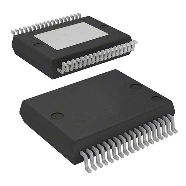


 工商网监
湘ICP备2023018690号
工商网监
湘ICP备2023018690号
