DG2501, DG2502, DG2503
www.vishay.com
Vishay Siliconix
200 , Low Leakage, Low Parasitic and Low Charge Injection,
Quad SPST Analog Switches
DESCRIPTION
FEATURES
The DG2501, DG2502, and DG2503 are monolithic quad
single-pole single-throw (SPST) analog switches that
operate from a single 1.8 V to 5.5 V power supply.
These switches are fully specified at 3 V and 5 V. The parts
feature low parasitic capacitance, low charge injection, and
low leakage performance over the full operating
temperature range of -40 °C to +85 °C. Their ESD/HBM
tolerance is over 8 kV.
The DG2501, DG2502, and DG2503 each feature four
independently selectable SPST switches with closely
matched channel resistance. The DG2501 is normally
closed, while the DG2502 is normally open.
The DG2503 has two normally open and two normally
closed
switches.
All
parts
are
guaranteed
break-before-make operation for use in multiplexer
applications. The parts have a guaranteed control logic high
of 1.4 V when V+ is 3 V and 1.8 V when V+ is 5 V.
Each switch conducts equally well in both directions when
on, and each has an input signal range that extends to the
supplies.
The DG2501, DG2502, and DG2503 are ideal for portable
healthcare, instrument, and communication devices.
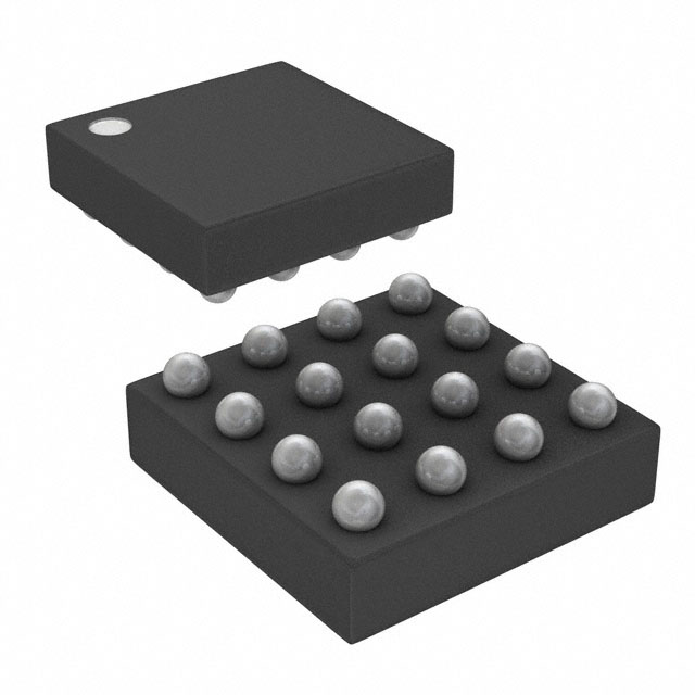
The DG2501, DG2502, and DG2503 are available in wafer
level CSP package with top side lamination.
The package has a 4 x 4 bump array, 0.35 mm pitch, and
1.44 mm x 1.44 mm length and width.
• 1.8 V to 5.5 V single supply operation
• Low leakage, 1 nA / max. at 85 °C
• Low switch off capacitance
• Rail-to-rail signal handling
• Latch up current > 800 mA (JESD78)
• ESD: 8000 V/HBM
• Typical power consumption (< 0.01 μW)
• TTL/CMOS compatible
• Compact WCSP16 1.44 mm x 1.44 mm
• Material categorization: for definitions of compliance
please see www.vishay.com/doc?99912
APPLICATIONS
• Analog front end signal switching
• Sample-and-hold circuits
• Battery-powered systems
• Portable meters
• Automatic test equipment
• Medical and healthcare equipment
• Communication systems
FUNCTIONAL BLOCK DIAGRAM
Switches are shown for a Logic 0 Input
TRUTH TABLE
DG2501
DG2502
DG2503
LOGIC
0
SWITCH
ON
LOGIC
0
SWITCH
OFF
LOGIC
0
SW1, SW4
OFF
SW2, SW3
ON
1
OFF
1
ON
1
ON
OFF
S17-1317-Rev. B, 21-Aug-17
Document Number: 62962
1
For technical questions, contact: analogswitchtechsupport@vishay.com
THIS DOCUMENT IS SUBJECT TO CHANGE WITHOUT NOTICE. THE PRODUCTS DESCRIBED HEREIN AND THIS DOCUMENT
ARE SUBJECT TO SPECIFIC DISCLAIMERS, SET FORTH AT www.vishay.com/doc?91000
�DG2501, DG2502, DG2503
www.vishay.com
Vishay Siliconix
ORDERING INFORMATION
PART NUMBER
CONFIGURATION
SWITCH
FUNCTION
TEMPERATURE
RANGE
PACKAGE
REEL
QUANTITY
DG2501DB-T2-GE1
Quad SPST
NC
-40 °C to +85 °C
WCSP16, 1.44 mm x 1.44 mm
3000
DG2501DB-T4-GE1
Quad SPST
NC
-40 °C to +85 °C
WCSP16, 1.44 mm x 1.44 mm
10 000
DG2502DB-T2-GE1
Quad SPST
NO
-40 °C to +85 °C
WCSP16, 1.44 mm x 1.44 mm
3000
DG2502DB-T4-GE1
Quad SPST
NO
-40 °C to +85 °C
WCSP16, 1.44 mm x 1.44 mm
10 000
DG2503DB-T2-GE1
Quad SPST
NC/NO
-40 °C to +85 °C
WCSP16, 1.44 mm x 1.44 mm
3000
DG2503DB-T4-GE1
Quad SPST
NC/NO
-40 °C to +85 °C
WCSP16, 1.44 mm x 1.44 mm
10 000
PACKAGE OUTLINE
A1
A2
GND
B1
D3
B2
S2
IN2
C1
C2
D2
IN1
D1
D2
S1
V+
A3
S3
B3
IN3
C3
IN4
D3
D1
A4
GND
B4
D4
Top View
(Bump Side Down)
C4
S4
D4
GND
Fig. 1 - Package Outline for WCSP16, 1.44 mm x 1.44 mm, 0.35 mm Pitch
DEVICE MARKING
1
2
3
4
A
B
C
Row 1 Dot = Pin A1 Locator
Row 2 B = Fab, 4 = Year, C = Week Code, A = Lot Code
Row 3 2501 = Part Code
D
Fig. 2 - Device Marking
ABSOLUTE MAXIMUM RATINGS
ELECTRICAL PARAMETERS
CONDITIONS
LIMITS
V+, INx
Reference to GND
-0.3 to +6
Sx, Dx
Reference to GND
-0.3 to (V+) +0.3
Maximum continuous switch current
5
Maximum peak current
(Pulsed 1 ms, 10 % duty cycle)
20
Thermal resistance
Latch up current
ESD - HBM
UNIT
V
mA
80
°C/W
JESD78
> 800
mA
ANSI / ESDA / JEDEC® JS-001
> 8000
V
Temperature
Operating temperature
-40 to +85
Storage temperature
-65 to +150
°C
Stresses beyond those listed under “Absolute Maximum Ratings” may cause permanent damage to the device. These are stress ratings only, and functional operation
of the device at these or any other conditions beyond those indicated in the operational sections of the specifications is not implied. Exposure to absolute maximum
rating conditions for extended periods may affect device reliability.
S17-1317-Rev. B, 21-Aug-17
Document Number: 62962
2
For technical questions, contact: analogswitchtechsupport@vishay.com
THIS DOCUMENT IS SUBJECT TO CHANGE WITHOUT NOTICE. THE PRODUCTS DESCRIBED HEREIN AND THIS DOCUMENT
ARE SUBJECT TO SPECIFIC DISCLAIMERS, SET FORTH AT www.vishay.com/doc?91000
�DG2501, DG2502, DG2503
www.vishay.com
Vishay Siliconix
ELECTRICAL CHARACTERISTICS 3 V Supply
PARAMETER
SYMBOL
TEST CONDITION
UNLESS OTHERWISE SPECIFIED,
V+ = 3 V
VINH = 1.4 V, VINL = 0.4 V a
-40 °C to +85 °C
TEMP.
b
TYP.
c
MIN. d
MAX. d
0
3
UNIT
Analog Switch
Analog signal range e
VANALOG
Drain-source on
resistance
RDS(on)
VS = 1.5 V, IS = -1 mA
On-resistance matching
Switch off leakage current
Channel on leakage
current
Ron
Full
-
Room
133
-
200
Full
-
-
250
Room
0.83
-
10
Full
-
-
13
± 0.016
-0.4
+0.4
IS/ID(off)
V+ = 3.3 V,
VS = 0.3 V/3 V, VD = 3 V / 0.3 V
Room
Full
-
-1
+1
ID(on)
V+ = 3.3 V,
VD = 0.3 V / 3 V
Room
± 0.009
-0.4
+0.4
Full
-
-1
+1
V
nA
Digital Control
Input, high voltage
VINH
Full
-
1.4
-
Input, low voltage
VINL
Full
-
-
0.4
Room
± 0.001
-
-
Full
-
-0.1
+0.1
-
-
Input leakage
IIN
VIN = VGND or V+
Digital input capacitance e
CIN
f = 1 MHz
Room
2
Break-before make time
tBBM
DG2503 only, VS1 = VS2 = 1.5 V,
RL = 300 CL = 35 pF
Room
47
10
-
Full
-
10
-
Turn-on time
tON
Room
175
-
220
Full
-
-
250
Room
77
-
100
Full
-
-
120
Room
-0.7
-
-
V
μA
pF
Dynamic Characteristics
VS = 1.5 V, RL = 300 , CL = 35 pF
Turn-off time
tOFF
Charge injection e
QINJ
Off isolation
e
OIRR
Cross talk e
X Talk
3 dB bandwidth e
BW
Source off capacitance
e
Room
-83
-
-
Room
-85
-
-
RL = 50 , CL = 5 pF
Room
510
-
-
Room
2.9
-
-
f = 1 MHz, VS = 1.5 V
Room
2.8
-
-
Room
7.8
-
-
Room
0.001
-
-
Full
-
-
1
RL = 50 , CL = 5 pF, f = 1MHz
CS(off)
Drain off capacitance e
CD(off)
e
CD(on)
Drain on capacitance
CL = 1 nF, RGEN = 0 , VS = 1.5 V
ns
pC
dB
MHz
pF
Power Requirements
Power supply current
S17-1317-Rev. B, 21-Aug-17
I+
Digital input 0 or V+
μA
Document Number: 62962
3
For technical questions, contact: analogswitchtechsupport@vishay.com
THIS DOCUMENT IS SUBJECT TO CHANGE WITHOUT NOTICE. THE PRODUCTS DESCRIBED HEREIN AND THIS DOCUMENT
ARE SUBJECT TO SPECIFIC DISCLAIMERS, SET FORTH AT www.vishay.com/doc?91000
�DG2501, DG2502, DG2503
www.vishay.com
Vishay Siliconix
ELECTRICAL CHARACTERISTICS 5 V Supply
PARAMETER
SYMBOL
TEST CONDITION
UNLESS OTHERWISE SPECIFIED,
V+ = 5 V
VINH = 1.8 V, VINL = 0.5 V a
-40 °C to +85 °C
TEMP. b
TYP. c
MIN. d
MAX. d
UNIT
Analog Switch
Analog signal range e
VANALOG
Drain-source on resistance
RDS(on)
VS = 2.5 V, IS = -1 mA
On-resistance matching
Switch off leakage current
Channel on leakage
current
Ron
Full
-
0
5
Room
104
-
150
Full
-
-
200
Room
0.39
-
8
Full
-
-
10
+0.4
IS/ID(off)
V+ = 5.5 V,
VS = 1 V/4.5 V, VD = 4.5 V/1 V
Room
± 0.022
-0.4
Full
-
-1
+1
ID(on)
V+ = 5.5 V,
VD = 4.5 V/1 V
Room
± 0.017
-0.4
+0.4
Full
-
-1
+1
V
nA
Digital Control
Input, high voltage
VINH
Full
-
1.8
-
Input, low voltage
VINL
Full
-
-
0.5
Room
± 0.001
-
-
Full
-
-1
+1
Input leakage
IIN
VIN = VGND or V+
Digital input capacitance e
CIN
f = 1 MHz
Room
2
-
-
tBBM
DG2503 only, VS1 = VS2 = 3 V,
RL = 300 CL = 35 pF
Room
25
10
-
Full
-
10
-
Room
64
-
100
Full
-
-
150
Room
38
-
60
Full
-
-
100
Room
-2
-
-
Room
-84
-
-
Room
-83
-
-
V
μA
pF
Dynamic Characteristics
Break-before make time
tON
Turn-on time
VS = 3 V, RL = 300 , CL = 35 pF
Turn-off time
tOFF
Charge injection e
QINJ
Off isolation
e
OIRR
Cross talk e
X Talk
3 dB bandwidth e
BW
Source off capacitance e
CS(off)
Drain off capacitance e
CD(off)
e
CD(on)
Drain on capacitance
CL = 1 nF, RGEN = 0 , VS = 3 V
RL = 50 , CL = 5 pF, f = 1MHz
RL = 50 , CL = 5 pF
f = 1 MHz, VS = 3 V
Room
550
-
-
Room
2.7
-
-
Room
2.6
-
-
Room
7.6
-
-
Room
4.6
-
-
Full
-
-
30
Room
0.001
-
-
Full
-
-
2
ns
pC
dB
MHz
pF
Power Requirements
Digital input = 1.8 V, at one channel
V+ = 5 V
Power supply current
I+
Digital input 0 or V+
μA
Notes
a. VIN = input voltage to perform proper function
b. Room = 25 °C, Full = as determined by the operating temperature suffix
c. Typical values are for DESIGN AID ONLY, not guaranteed nor subject to production testing
d. The convention where the most negative value is a minimum and the most positive a maximum, is used in this data sheet
e. Guaranteed by design, not subject to production test
S17-1317-Rev. B, 21-Aug-17
Document Number: 62962
4
For technical questions, contact: analogswitchtechsupport@vishay.com
THIS DOCUMENT IS SUBJECT TO CHANGE WITHOUT NOTICE. THE PRODUCTS DESCRIBED HEREIN AND THIS DOCUMENT
ARE SUBJECT TO SPECIFIC DISCLAIMERS, SET FORTH AT www.vishay.com/doc?91000
�DG2501, DG2502, DG2503
www.vishay.com
Vishay Siliconix
TYPICAL CHARACTERISTICS (TA = 25 °C, unless otherwise noted)
400
150
V+ = +1.8V
350
V+ = +3.0V
250
V+ = +4.5V
200
130
RON - On-Resistance (Ω)
300
RON - On-Resistance (Ω)
+ 125 °C
140
V+ = +2.7V
V+ = +5.0V
150
100
120
110
100
TA = +25 °C
50
+ 85 °C
0
+ 25 °C
V+ = +5 V
IS = -1 mA
90
IS = -1 mA
80
0.0
1.0
2.0
3.0
4.0
5.0
0
1
2
3
VD - Analog Voltage (V)
VD - Analog Voltage (V)
180
5
1500
+ 125 °C
170
160
+ 85 °C
150
140
+ 25 °C
130
120
V+ = +3 V
IS = -1 mA
110
ID(OFF),
VD= 4.5V,VS=1V
,
ID(ON), VD=4.5V
1000
Leakage Current (pA)
RON - On-Resistance (Ω)
4
On-Resistance vs. Analog Voltage
On-Resistance vs. Analog Voltage
- 40 °C
500
IS(OFF)
VS= 4.5V,VD=1V
0
-500
ID(ON), VD=1V
-1000
ID(OFF),
VD = 1 V, VS = 4.5 V
-1500
V+= + 5.5 V
-2000
100
0.0
0.5
1.0
1.5
2.0
2.5
3.0
-40
-20
0
VD - Analog Voltage (V)
IS(OFF),
VS = 1 V, VD = 4.5 V
20
40
60
Temperature (°C)
80
100
120
Leakage Current vs. Temperature
On-Resistance vs. Analog Voltage
1000
50
ID(OFF),
VD= 3V,VS=0.3V
ID(ON), VD=3V
IS(OFF)
VS= 3V,VD=0.3V
0
-500
ID(ON), VD=0.3V
ID(OFF),
VD= 0.3V,VS=3V
-1000
V+ = +5V
IN = V+ or GND
40
I+ - Supply Current (nA)
500
Leakage Current (pA)
- 40 °C
30
V+ = +3V
IN = V+ or GND
20
10
IS(OFF)
VS= 0.3V,VD=3V
V+= + 3.3 V
-1500
0
-40
-20
0
20
40
60
80
100
Temperature (°C)
Leakage Current vs. Temperature
S17-1317-Rev. B, 21-Aug-17
120
-40
-20
0
20
40
60
80
100
120
Temperature (°C)
Supply Current vs. Temperature
Document Number: 62962
5
For technical questions, contact: analogswitchtechsupport@vishay.com
THIS DOCUMENT IS SUBJECT TO CHANGE WITHOUT NOTICE. THE PRODUCTS DESCRIBED HEREIN AND THIS DOCUMENT
ARE SUBJECT TO SPECIFIC DISCLAIMERS, SET FORTH AT www.vishay.com/doc?91000
�DG2501, DG2502, DG2503
www.vishay.com
Vishay Siliconix
6
1000
5.5
100
I+ - Supply Current (μA)
I+ - Supply Current (μA)
TYPICAL CHARACTERISTICS (TA = 25 °C, unless otherwise noted)
5
4.5
4
V+ = +5V
ONE INPUT = 1.8V
OTHER INPUTS = GND or V+
3.5
TA = +25 °C
I+ PER LOGIC INPUT
V+ = +5 V
10
1
0.1
0.01
0.001
3
0.0001
-40
-20
0
20
40
60
80
100
120
0
1
2
1000
5
0.0
TA = +25 °C
I+ PER LOGIC INPUT
V+ = +3 V
100
- 0.5
10
QINJ - Charge Injection (pC)
I+ - Supply Current (μA)
4
Supply Current vs. VIN
Supply Current vs. Temperature
1
0.1
0.01
0.001
V+ = 1.8 V
- 1.0
V+ = 3 V
- 1.5
V+ = 5 V
- 2.0
- 2.5
- 3.0
0.0001
0.00001
- 3.5
0.0
0.5
1.0
1.5
2.0
2.5
3.0
VIN (V)
0
2
3
VS - Analog Voltage (V)
Supply Current vs. VIN
Charge Injection vs. Analog Voltage
200
180
0
140
100
V+ = +5 V, tON
V+ = +3 V, tOFF
V+ = +3V, tBBM
80
60
5
Loss
- 20
- 30
V+ = +5 V
RL = 50 Ω
- 40
- 50
OIRR
- 60
XTALK
- 70
- 80
40
- 90
20
0
- 40
4
- 10
160
120
1
10
V+ = +3 V, tON
Loss, OIRR, XTALK (dB)
tON, tOFF,tBBM - Switching Time (ns)
3
VIN (V)
Temperature (°C)
V+ = +5 V, tBBM
V+ = +5 V, tOFF
- 100
- 110
- 20
0
20
40
60
80
100
Temperature (°C)
Switching Time vs. Temperature
S17-1317-Rev. B, 21-Aug-17
120
100K
1M
10M
Frequency (Hz)
100M
1G
Loss, OIRR, XTALK vs. Frequency
Document Number: 62962
6
For technical questions, contact: analogswitchtechsupport@vishay.com
THIS DOCUMENT IS SUBJECT TO CHANGE WITHOUT NOTICE. THE PRODUCTS DESCRIBED HEREIN AND THIS DOCUMENT
ARE SUBJECT TO SPECIFIC DISCLAIMERS, SET FORTH AT www.vishay.com/doc?91000
�DG2501, DG2502, DG2503
www.vishay.com
Vishay Siliconix
TYPICAL CHARACTERISTICS (TA = 25 °C, unless otherwise noted)
1.0
10
0
TA = +25 °C
Loss
0.9
VT - Logic Threshold (V)
Loss, OIRR, XTALK (dB)
- 10
VIH
- 20
V+ = +3 V
RL = 50 Ω
- 30
- 40
- 50
OIRR
- 60
XTALK
- 70
VIL
0.8
0.7
- 80
0.6
- 90
- 100
0.5
- 110
100K
1M
10M
Frequency (Hz)
1G
100M
1
2
2.5
3
3.5
4
4.5
5
5.5
V+ - Supply Voltage (V)
Logic Threshold vs. Supply Voltage
Loss, OIRR, XTALK vs. Frequency
1000
10 000
V+ = +5 V
TA = +25 °C
100
I+ - Supply Current (μA)
1.5
V+ = +3 V
TA = +25 °C
1000
I+ - Supply Current (μA)
10
1
0.1
0.01
0.001
0.0001
100
10
1
0.1
0.01
0.001
0.00001
0.0001
10
100
1000
10K
100K
1M
Input Switching Frequency (Hz)
10M
Supply Current vs. Input Switching Frequency
10
100
1000
10K
100K
1M
Input Switching Frequency (Hz)
10M
Supply Current vs. Input Switching Frequency
10 000
V+ = +5.0 V
One Input = 0 V to +1.8 V
TA = +25 °C
I+ - Supply Current (μA)
1000
100
10
1
0.1
10
100
1000
10K
100K
1M
10M
Input Switching Frequency (Hz)
Supply Current vs. Input Switching Frequency
S17-1317-Rev. B, 21-Aug-17
Document Number: 62962
7
For technical questions, contact: analogswitchtechsupport@vishay.com
THIS DOCUMENT IS SUBJECT TO CHANGE WITHOUT NOTICE. THE PRODUCTS DESCRIBED HEREIN AND THIS DOCUMENT
ARE SUBJECT TO SPECIFIC DISCLAIMERS, SET FORTH AT www.vishay.com/doc?91000
�DG2501, DG2502, DG2503
www.vishay.com
Vishay Siliconix
TEST CIRCUIT
V+
VINH
Logic
Input
VINL
V+
S
Switch
Input
tr < 5 ns
tf < 5 ns
50 %
Switch Output
D
VOUT
0.9 x VOUT
Switch
Output
IN
Logic
Input
RL
300 Ω
GND
CL
35 pF
0V
tON
Logic "1" = Switch On
Logic input waveforms inverted for switches that have
the opposite logic sense.
CL (includes fixture and stray capacitance)
RL
V OUT = V D
tOFF
R L + R ON
Fig. 3 - Switching Time
V+
V OUT
V+
Rgen
D
VOUT
S
VOUT
+
IN
Vgen
IN
CL = 1 nF
On
On
Off
GND
Q = V OUT x CL
VIN = 0 - V+
IN depends on switch configuration: input polarity
determined by sense of switch.
Fig. 4 - Charge Injection
V+
V+
10 nF
10 nF
V+
V+
S
IN
D
0 V, 2.4 V
Meter
D
IN
0 V, 2.4 V
RL
S
GND
HP4192A
Impedance
Analyzer
or Equivalent
GND
f = 1 MHz
Analyzer
Off Isolation = 20 log
Fig. 5 - Off-Isolation
VD
VS
Fig. 6 - Channel Off/On Capacitance
Vishay Siliconix maintains worldwide manufacturing capability. Products may be manufactured at one of several qualified locations. Reliability data for Silicon
Technology and Package Reliability represent a composite of all qualified locations. For related documents such as package / tape drawings, part marking, and
reliability data, see www.vishay.com/ppg?62962.
S17-1317-Rev. B, 21-Aug-17
Document Number: 62962
8
For technical questions, contact: analogswitchtechsupport@vishay.com
THIS DOCUMENT IS SUBJECT TO CHANGE WITHOUT NOTICE. THE PRODUCTS DESCRIBED HEREIN AND THIS DOCUMENT
ARE SUBJECT TO SPECIFIC DISCLAIMERS, SET FORTH AT www.vishay.com/doc?91000
�Package Information
www.vishay.com
Vishay Siliconix
WCSP 4 x 4: 16 Bumps
(4 x 4, 0.35 mm pitch, 172 μm bump height, 1.48 mm x 1.48 mm die size)
Index Bump A1
D4
C4
B4
S4
A4
GND
D4
FYWL
ABCD
e
GND
s
16xØ b
D3
B3
C3
A3
S3
IN3
IN4
D
e
D1
D2
C2
S1
IN1
D1
C1
B1
V+
D2
S2
B2
A2
D3
e
IN2
A1
s
GND
s
E
e
e
e
s
Bottom View
Top View
16 x Ø 0.15 mm Cu pad
A
A1
Note 3
Bump Note 2
Side View
e
e
e
A1
Note 4
Solder mask Ø 0.25 mm
e
e
e
Recommended Land Pattern (NSMD)
DWG: 6022
Notes
(1) Laser mark on the silicon die back, coated with an epoxy film
(2) Bumps are SAC405
(3) 0.05 max. co-planarity
(4) Laminate tape thickness is 0.022 mm
DIM.
MILLIMETERS a
INCHES
MIN.
NOM.
MAX.
MIN.
NOM.
MAX.
A
0.444
0.474
0.504
0.0175
0.0187
0.0198
A1
0.146
0.172
0.198
0.0057
0.0068
0.0078
b
0.165
0.205
0.245
0.0065
0.0081
0.0096
e
0.350
0.0138
s
0.175
0.195
0.215
0.0069
0.0077
0.0085
D
1.400
1.440
1.480
0.0551
0.0567
0.0583
E
1.400
1.440
1.480
0.0551
0.0567
0.0583
Note
a. Use millimeters as the primary measurement.
S14-0644-Rev. A, 31-Mar-14
Document Number: 64347
1
For technical questions, contact: powerictechsupport@vishay.com
THIS DOCUMENT IS SUBJECT TO CHANGE WITHOUT NOTICE. THE PRODUCTS DESCRIBED HEREIN AND THIS DOCUMENT
ARE SUBJECT TO SPECIFIC DISCLAIMERS, SET FORTH AT www.vishay.com/doc?91000
�Legal Disclaimer Notice
www.vishay.com
Vishay
Disclaimer
ALL PRODUCT, PRODUCT SPECIFICATIONS AND DATA ARE SUBJECT TO CHANGE WITHOUT NOTICE TO IMPROVE
RELIABILITY, FUNCTION OR DESIGN OR OTHERWISE.
Vishay Intertechnology, Inc., its affiliates, agents, and employees, and all persons acting on its or their behalf (collectively,
“Vishay”), disclaim any and all liability for any errors, inaccuracies or incompleteness contained in any datasheet or in any other
disclosure relating to any product.
Vishay makes no warranty, representation or guarantee regarding the suitability of the products for any particular purpose or
the continuing production of any product. To the maximum extent permitted by applicable law, Vishay disclaims (i) any and all
liability arising out of the application or use of any product, (ii) any and all liability, including without limitation special,
consequential or incidental damages, and (iii) any and all implied warranties, including warranties of fitness for particular
purpose, non-infringement and merchantability.
Statements regarding the suitability of products for certain types of applications are based on Vishay’s knowledge of
typical requirements that are often placed on Vishay products in generic applications. Such statements are not binding
statements about the suitability of products for a particular application. It is the customer’s responsibility to validate that a
particular product with the properties described in the product specification is suitable for use in a particular application.
Parameters provided in datasheets and / or specifications may vary in different applications and performance may vary over
time. All operating parameters, including typical parameters, must be validated for each customer application by the customer’s
technical experts. Product specifications do not expand or otherwise modify Vishay’s terms and conditions of purchase,
including but not limited to the warranty expressed therein.
Except as expressly indicated in writing, Vishay products are not designed for use in medical, life-saving, or life-sustaining
applications or for any other application in which the failure of the Vishay product could result in personal injury or death.
Customers using or selling Vishay products not expressly indicated for use in such applications do so at their own risk.
Please contact authorized Vishay personnel to obtain written terms and conditions regarding products designed for
such applications.
No license, express or implied, by estoppel or otherwise, to any intellectual property rights is granted by this document
or by any conduct of Vishay. Product names and markings noted herein may be trademarks of their respective owners.
© 2017 VISHAY INTERTECHNOLOGY, INC. ALL RIGHTS RESERVED
Revision: 08-Feb-17
1
Document Number: 91000
�


 工商网监
湘ICP备2023018690号
工商网监
湘ICP备2023018690号
