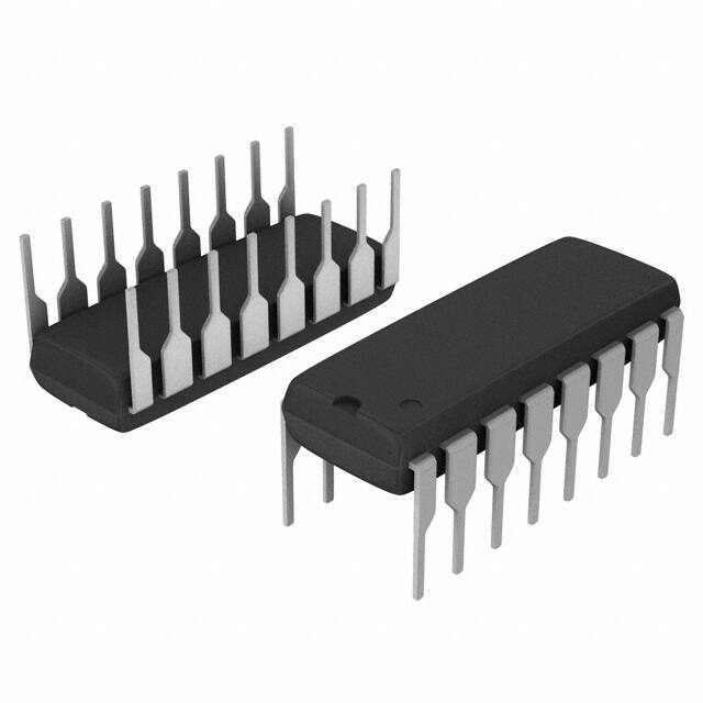
DG458, DG459
Vishay Siliconix
Fault-Protected Single 8-Ch/Differential 4-Ch Analog Multiplexers
DESCRIPTION
FEATURES
The DG458 and DG459 are 8-channel single-ended and
•
•
•
•
•
•
•
•
4-channel differential analog multiplexers, respectively,
incorporating fault protection. A series n-p-n MOSFET
structure provides device and signal-source protection in the
event of power loss or overvoltages. Under fault conditions
the multiplexer input (or output) appears as an open circuit
and only a few nanoamperes of leakage current will flow.
Fault and Overvoltage Protection
All Channels Off When Power Off
Latchup-Proof
Fast Switching - tA: 200 ns
Break-Before-Make Switching
Low On-Resistance: 180 W
Low Power Consumption: 3 mW
TTL and CMOS Compatible Inputs
This protects not only the multiplexer and the circuitry
following it, but also protects the sensors or signal sources
BENEFITS
which drive the multiplexer.
•
•
•
•
•
•
The DG458 and DG459 can withstand continuous
overvoltage inputs up to ± 35 V. All digital inputs have TTL
compatible logic thresholds. Break-before-make operation
prevents channel-to-channel interference.
The DG458 and DG459 are improved pin-compatible
replacements
for
HI-508A/509A
and
MAX358/359
multiplexers.
Improved Ruggedness
Power Loss Protection
Prevents Adjacent Channel Crosstalk
Standard Logic Interface
Superior Accuracy
Fast Settling Time
APPLICATIONS
•
•
•
•
•
Data Acquisition Systems
Industrial Process Control Systems
Avionics Test Equipment
High-Rel Control Systems
Telemetry
FUNCTIONAL BLOCK DIAGRAM AND PIN CONFIGURATION
DG459
DG458
Dual-In-Line
Dual-In-Line
A0
EN
VS1
S2
S3
S4
D
16
1
2
Decoders/Drivers
15
3
14
4
13
5
12
6
11
7
10
8
9
A1
A0
A2
EN
GND
V-
V+
S1a
S5
S2a
S6
S3a
S7
S4a
S8
Da
Top View
16
1
2
Decoders/Drivers
15
3
14
4
13
5
12
6
11
7
10
8
9
A1
GND
V+
S1b
S2b
S3b
S4b
Db
Top View
* Pb containing terminations are not RoHS compliant, exemptions may apply
Document Number: 70064
S11-1029–Rev. H, 23-May-11
www.vishay.com
1
This document is subject to change without notice.
THE PRODUCTS DESCRIBED HEREIN AND THIS DOCUMENT ARE SUBJECT TO SPECIFIC DISCLAIMERS, SET FORTH AT www.vishay.com/doc?91000
�DG458, DG459
Vishay Siliconix
THRU TABLES AND ORDERING INFORMATION
TRUTH TABLE - DG458
TRUTH TABLE - DG459
A2
A1
A0
EN
On Switch
A1
A0
EN
On Switch
X
X
X
0
None
X
X
0
None
0
0
0
1
1
0
0
1
1
0
0
1
1
2
0
1
1
2
0
1
0
1
3
1
0
1
3
0
1
1
1
4
1
1
1
4
1
0
0
1
5
1
0
1
1
6
1
1
0
1
7
1
1
1
1
8
Logic "0" = VAL 0.8 V
Logic "1" = VAH 2.4 V
X = Don’t Care
ORDERING INFORMATION
Temp Range
Package
Part Number
DG458DJ
DG458DJ-E3
- 40 to 85 °C
16-pin Plastic DIP
DG459DJ
DG459DJ-E3
ABSOLUTE MAXIMUM RATINGS
Parameter
Limit
V+ to V-
Unit
44
V+ to GND
22
V- to GND
VEN, VA Digital Input
- 25
(V-) - 4 to (V+) + 4
VS, Analog Input Overvoltage with Power On
(V-) - 20 to (V+) + 20
VS, Analog Input Overvoltage with Power Off
- 35 to + 35
Continuous Current, S or D
20
Peak Current, S or D (Pulsed at 1 ms, 10 % duty cycle max)
40
Storage Temperature
a
Power Dissipation (Package)
(AK Suffix)
- 65 to 150
(DJ Suffix)
- 65 to 125
16-pin Plastic DIPB
600
16-pin CerDIPC
1000
LCC-20d
1000
V
mA
°C
mW
Notes:
a. All leads soldered or welded to PC board.
b. Derate 6.3 mW/°C above 75 °C.
c. Derate 12 mW/°C above 75 °C.
d. Derate 10 mW/°C above 75 °C.
www.vishay.com
2
Document Number: 70064
S11-1029–Rev. H, 23-May-11
This document is subject to change without notice.
THE PRODUCTS DESCRIBED HEREIN AND THIS DOCUMENT ARE SUBJECT TO SPECIFIC DISCLAIMERS, SET FORTH AT www.vishay.com/doc?91000
�DG458, DG459
Vishay Siliconix
SPECIFICATIONSa
Test Conditions
Unless Otherwise Specified
V+ = 15 V, V- = - 15 V
VAL = 0.8 V, VAH = 2.4 Vf
A Suffix
D Suffix
- 55 °C to 125 °C - 40 °C to 85 °C
Temp.b
Parameter
Analog Switch
Symbol
Analog Signal Rangee
VANALOG
Full
RDS(on)
Room
Full
Room
Drain-Source
On-Resistance
VD = ± 9.5 V, IS = - 400 µA
VD = ± 5 V, IS = - 400 µA
Typ.c
Min.d
- 10
0.45
Max.d
Min.d
10
- 10
Unit
10
V
1.5
1.8
400
1.2
1.5
400
180
Max.d
RDS(on)
VD = 0 V, IS = - 400 µA
Room
6
Source Off Leakage Current
IS(off)
VEN = 0 V, VD = ± 10 V
VS = ± 10 V
Room
Full
0.03
- 0.5
- 50
0.5
50
-1
- 20
1
20
Drain Off Leakage Current
Room
Full
Room
Full
0.1
ID(off)
-1
- 200
-1
- 100
1
200
1
100
-1
- 50
-2
- 25
1
50
2
25
- 50
50
- 20
20
-2
- 200
-2
- 100
2
200
2
100
-5
- 50
-5
- 25
5
50
5
25
h
RDS(on) Matching Between Channels
Differential Off Drain
Leakage Current
IDIFF
VEN = 0 V
VD = ± 10 V
VS = ± 10 V
DG458
DG459
DG459 Only
Room
DG458
Drain On Leakage Current
ID(on)
0.1
VS = VD = ± 10 V
DG459
Room
Full
Room
Full
0.1
0.05
k
%
nA
Fault
Output Leakage Current
(with Overvoltage)
Input Leakage Current
(with Overvoltage)
Input Leakage Current
(with Power Supplies Off)
ID(off)
IS(off)
VS = ± 33 V, VD = 0 V
See Figure 1
VS = ± 25 V, VD = 10 V,
See Figure 1
VS = ± 25 V, VSUPS = 0 V
VD = A0, A1, A2, EN = 0 V
Room
0.02
nA
Room
0.005
-5
5
- 10
10
Room
0.001
-2
2
-5
5
µA
Digital Control
Input Low Threshold
VAl
Full
Input Low Threshold
VAL
Full
2.4
Full
-1
Logic Input Control
Document Number: 70064
S11-1029–Rev. H, 23-May-11
IA
VA = 2.4 V or 0.8 V
0.8
0.8
2.4
1
-1
1
V
µA
www.vishay.com
3
This document is subject to change without notice.
THE PRODUCTS DESCRIBED HEREIN AND THIS DOCUMENT ARE SUBJECT TO SPECIFIC DISCLAIMERS, SET FORTH AT www.vishay.com/doc?91000
�DG458, DG459
Vishay Siliconix
SPECIFICATIONSa
Parameter
Dynamic Characteristics
Symbol
Test Conditions
Unless Otherwise Specified
V+ = 15 V, V- = - 15 V
VAL = 0.8 V, VAH = 2.4 Vf
Temp.b
Typ.c
A Suffix
D Suffix
- 55 °C to 125 °C - 40 °C to 85 °C
tA
See Figure 3
Room
200
Break-Before-Make Interval
tOPEN
See Figure 4
Room
45
Enable Turn-On Time
tON(EN)
Room
Full
Room
Full
Room
140
Room
1.5
Room
90
Room
5
Transition Time
See Figure 5
Enable Turn-Off Time
tOFF(EN)
Settling Time
ts
Off Isolation
OIRR
Logic Input Capacitance
Cin
Source Off Capacitance
CS(off)
Drain Off Capacitance
CD(off)
Drain On Capacitance
CD(on)
To 0.1 %
To 0.01 %
VEN = 0 V, RL = 1 k
CL = 15 pF, VS = 3 VRMS
f = 100 kHz
f = 1 MHz
Min.d
Max.d
Min.d
500
10
500
250
500
250
500
0.5
Room
5
DG458
Room
15
DG459
Room
10
DG458
Room
40
DG459
Room
35
Room
Full
Room
Full
0.05
Unit
10
250
500
250
500
50
Max.d
ns
µs
dB
pF
Power Supplies
Positive Supply Current
I+
Negative Supply Current
I-
VEN = 5 or 0 V, VA = 0 V
Power Supply Range for
Continuous Operation
Room
- 0.01
0.1
0.2
0.1
0.2
- 0.1
- 0.2
± 4.5
- 0.1
- 0.2
± 18
± 4.5
± 18
mA
V
Notes:
a. Refer to PROCESS OPTION FLOWCHART.
b. Room = 25 °C, Full = as determined by the operating temperature suffix.
c. Typical values are for DESIGN AID ONLY, not guaranteed nor subject to production testing.
d. The algebraic convention whereby the most negative value is a minimum and the most positive a maximum, is used in this data sheet.
e. Guaranteed by design, not subject to production test.
f. VIN = input voltage to perform proper function.
g. When the analog signal exceeds the + 13.5 V or - 12 V,RDS(on) starts to rise until only leakage currents flow.
RDS(on) MAX - RDS(on) MIN
x 100 %
h. RDS(on) =
RrDS(on) AVE
(
)
Stresses beyond those listed under “Absolute Maximum Ratings” may cause permanent damage to the device. These are stress ratings only, and functional operation
of the device at these or any other conditions beyond those indicated in the operational sections of the specifications is not implied. Exposure to absolute maximum
rating conditions for extended periods may affect device reliability.
www.vishay.com
4
Document Number: 70064
S11-1029–Rev. H, 23-May-11
This document is subject to change without notice.
THE PRODUCTS DESCRIBED HEREIN AND THIS DOCUMENT ARE SUBJECT TO SPECIFIC DISCLAIMERS, SET FORTH AT www.vishay.com/doc?91000
�DG458, DG459
Vishay Siliconix
TYPICAL CHARACTERISTICS (25 °C, unless otherwise noted)
1 mA
700
RDS(on) – Drain-Source On-Resistance ( )
V+ = V- = 0 V
100 µA
I S – Source Current
10 µA
1 µA
100 nA
10 nA
Operating Range
1 nA
100 pA
10 pA
1 pA
- 50 - 40 - 30 - 20 - 10
0
10
20
30
40
V+ = 15 V
V- = - 15 V
600
500
25 °C
400
85 °C
300
200
100
- 55 °C
0
50
- 10 - 7.5
- 5.0
VS – Source Voltage (V)
- 2.5
2.5
0
7.5
5.0
10
VD – Drain Voltage (V)
RDS(on) vs. VD and Temperature
Input Leakage vs. Input Voltage
1 mA
10
V+ = 15 V
V- = - 15 V
VS, VD = ± 10 V
V+ = 15 V
V- = - 15 V
100 µA
10 µA
1 µA
I S, I D (nA)
I S – Source Current
125 °C
0 °C
100 nA
10 nA
Operating Range
ID(on)
1
ID(off)
IS(off)
1 nA
0.10
100 pA
10 pA
1 pA
- 50 - 40 - 30 - 20 - 10
0.01
0
10
20
30
40
50
- 55 - 35 - 15
VS – Source Voltage (V)
25
45
65
85
105
125
Temperature (°C)
Leakage Currents vs. Temperature
Off-Channel Leakage Currents vs. Input Voltage
2000
1 nA
R DS(on) Drain-Source On-Resistance ( )
V+ = 15 V
V- = - 15 V
100 pA
I D – Drain Current
5
10 pA
1 pA
0.1 pA
- 50 - 40 - 30 - 20 - 10
0
10
20
30
40
VS – Source Voltage (V)
Output Leakage vs. Off-Channel Overvoltage
Document Number: 70064
S11-1029–Rev. H, 23-May-11
50
1600
± 5V
Supplies
1200
± 10 V
800
± 15 V
400
± 20 V
0
- 20
- 15
- 10
-5
0
5
10
15
20
25
VS – Source Voltage (V)
RDS(on) vs. Input Voltage
www.vishay.com
5
This document is subject to change without notice.
THE PRODUCTS DESCRIBED HEREIN AND THIS DOCUMENT ARE SUBJECT TO SPECIFIC DISCLAIMERS, SET FORTH AT www.vishay.com/doc?91000
�DG458, DG459
Vishay Siliconix
TYPICAL CHARACTERISTICS (25 °C, unless otherwise noted)
- 110
25
V+ = 15 V
V- = - 15 V
20
IS(off)
10
- 90
ID(off)
5
(dB)
I S, I D – Leakage (pA)
15
V+ = 15 V
V- = - 15 V
RL = 1 kΩ
- 100
0
- 80
Off Isolation
-5
ID(on)
- 10
Crosstalk
- 70
- 15
- 60
- 20
- 50
- 25
- 15 - 12 - 9
-6
-3
1
3
6
9
12
15
10 k
Leakage Current vs. VS, VD
Off Isolation and XTALK vs. Frequency
0
tTRANS
V+ = 15 V
V- = - 15 V
- 10
Charge Injection (pC)
200
Time (ns)
10 M
f – Frequency (Hz)
240
160
tON(EN)
120
VIN = 2 V
80
- 20
- 30
CL = 1 nF
- 40
- 50
tOFF(EN)
CL = 10 nF
- 60
40
±5
± 10
± 15
- 10
± 20
-5
0
5
10
VS – Source Voltage (V)
V+, V- – Positive and Negative Supplies (V)
Switching Times (tTRANS, tON, tOFF) vs. ± VSUPPLIES
QINJ vs. VS
280
3.0
V+ = 15 V
V- = - 15 V
240
2.5
tTRANS
200
2.0
tON(EN)
160
V TH (V)
Time (ns)
1M
100 k
VD or VS – Drain or Source Voltage (V)
120
tOPEN
1.5
1.0
80
0.5
tOFF(EN)
40
0
0
- 55 - 35 - 15
5
25
45
65
85
105
Temperature (°C)
Switching Times vs. Temperature
www.vishay.com
6
125
2.5
5
7.5
10
12.5
15
17.5
20
V+, Supply (V)
Logic Input Switching Threshold vs. ± VSUPPLIES
Document Number: 70064
S11-1029–Rev. H, 23-May-11
This document is subject to change without notice.
THE PRODUCTS DESCRIBED HEREIN AND THIS DOCUMENT ARE SUBJECT TO SPECIFIC DISCLAIMERS, SET FORTH AT www.vishay.com/doc?91000
�DG458, DG459
Vishay Siliconix
SCHEMATIC DIAGRAM (TYPICAL CHANNEL)
V+
VVREF
GND
D
V+
A0
VV+
Level
Shift
AX
Decode/
Drive
S1
VV+
EN
Sn
V-
TEST CIRCUITS
+ 15 V
V+
IS(off)
± VS
ID(off)
Sn
A
D
A
VD
V-
- 15 V
Figure 2. Analog Input Overvoltage
+ 15 V
+ 2.4 V
V+
EN
S1b
*
A2
A1
Logic
Input
±5V
DG458
A0
S8b
± 5V
VO
Switch
Output
VO
V-
50 Ω
1 MΩ
50 %
0V
Db
GND
3V
35 pF
+5V
90 %
-5V
tA
- 15 V
* = S1a - S 8a, S2b - S 7b, Da
Figure 3. Transition Time
Document Number: 70064
S11-1029–Rev. H, 23-May-11
www.vishay.com
7
This document is subject to change without notice.
THE PRODUCTS DESCRIBED HEREIN AND THIS DOCUMENT ARE SUBJECT TO SPECIFIC DISCLAIMERS, SET FORTH AT www.vishay.com/doc?91000
�DG458, DG459
Vishay Siliconix
TEST CIRCUITS
+ 15 V
V+
EN
+ 2.4 V
S1 , S8
Logic
Input
+5V
3V
0V
S2 - S 7
A0
DG458
A1
A2
Db, D
GND
Switch
Output
VO
V-
50 Ω
50 %
VO
1 kΩ
- 15 V
0V
35 pF
tOPEN
Figure 4. Break-Before-Make Time
+ 15 V
V+
S1
Enable
Input
+5V
EN
S2 - S 8
VS
DG458
A2
GND
50 %
0V
A0
A1
3V
V-
50 Ω
Switch
Output
D
1 kΩ
VO
35 pF
VO
90 %
0V
tON(EN)
tOF
- 15 V
Figure 5. Enable Delay
www.vishay.com
8
Document Number: 70064
S11-1029–Rev. H, 23-May-11
This document is subject to change without notice.
THE PRODUCTS DESCRIBED HEREIN AND THIS DOCUMENT ARE SUBJECT TO SPECIFIC DISCLAIMERS, SET FORTH AT www.vishay.com/doc?91000
�DG458, DG459
Vishay Siliconix
DETAILED DESCRIPTION
The Vishay Siliconix DG458 and DG459 multiplexers are
fully fault- and overvoltage-protected for continuous input
voltages up to ± 35 V whether or not voltage is applied to the
power supply pins (V+, V-). These multiplexers are built on a
high-voltage junction-isolated silicon-gate CMOS process.
Two n-channel and one p-channel MOSFETs are connected
in series to form each channel (Figure 1).
Within the normal analog signal range (± 10 V), the RDS(on)
variation as a function of analog signal voltage is comparable
to that of the classic parallel N-MOS and P-MOS switches.
- 35 V
Overvoltage
n-Channel
MOSFET
is On
Q1 - 35 V
S
D
G
Q2
S
D
G
Q3
S
+ 35 V
Overvoltage
D
n-Channel
MOSFET
is Off
G
p-Channel
MOSFET
is Off
(a) Overvoltage with Multiplexer Power Off
When the analog signal approaches or exceeds either
supply rail, even for an on-channel, one of the three series
MOSFETs gets cut-off, providing inherent protection against
overvoltages even if the multiplexer power supply voltages
are lost. This protection is good up to the breakdown voltage
of the respective series MOSFETs. Under fault conditions
only sub microamp leakage currents can flow in or out of the
multiplexer. This not only provides protection for the
multiplexer and succeeding circuitry, but it allows normal,
undisturbed operation of all other channels. Additionally, in
case of power loss to the multiplexer, the loading caused on
the transducers and signal sources is insignificant, therefore
redundant multiplexers can be used on critical applications
such as telemetry and avionics.
- 15 V
Q1
- 35 V
Overvoltage
n-Channel
MOSFET
is On
+ 15 V
- 15 V
Q2
+ 15 V
- 15 V
Q3
+ 35 V
Overvoltage
n-Channel
MOSFET
is Off
p-Channel
MOSFET
is Off
(b) Overvoltage with Multiplexer Power On
Figure 5. Overvoltage Protection
Vishay Siliconix maintains worldwide manufacturing capability. Products may be manufactured at one of several qualified locations. Reliability data for Silicon Technology and Package Reliability represent a composite of all qualified locations. For related documents such as package/tape drawings, part marking, and reliability
data, see http://www.vishay.com/ppg?70064.
Document Number: 70064
S11-1029–Rev. H, 23-May-11
www.vishay.com
9
This document is subject to change without notice.
THE PRODUCTS DESCRIBED HEREIN AND THIS DOCUMENT ARE SUBJECT TO SPECIFIC DISCLAIMERS, SET FORTH AT www.vishay.com/doc?91000
�Package Information
Vishay Siliconix
PDIP: 16ĆLEAD
16
15
14
13
12
11
10
9
E
E1
1
2
3
4
5
6
7
8
D
S
Q1
A
A1
L
15°
MAX
C
B1
e1
Dim
A
A1
B
B1
C
D
E
E1
e1
eA
L
Q1
S
B
eA
MILLIMETERS
Min
Max
INCHES
Min
Max
3.81
5.08
0.150
0.200
0.38
1.27
0.015
0.050
0.38
0.51
0.015
0.020
0.89
1.65
0.035
0.065
0.20
0.30
0.008
0.012
18.93
21.33
0.745
0.840
7.62
8.26
0.300
0.325
5.59
7.11
0.220
0.280
2.29
2.79
0.090
0.110
7.37
7.87
0.290
0.310
2.79
3.81
0.110
0.150
1.27
2.03
0.050
0.080
0.38
1.52
.015
0.060
ECN: S-03946—Rev. D, 09-Jul-01
DWG: 5482
Document Number: 71261
06-Jul-01
www.vishay.com
1
�Package Information
Vishay Siliconix
CERDIP: 16ĆLEAD
16
15
14
13
12
11
10
9
E1 E
1
2
3
4
5
6
7
8
D
S
Q1
A
A1
L1
L
e1
C
B
B1
MILLIMETERS
Dim
A
A1
B
B1
C
D
E
E1
e1
eA
L
L1
Q1
S
∝
eA
INCHES
Min
Max
Min
Max
4.06
5.08
0.160
0.200
0.51
1.14
0.020
0.045
0.38
0.51
0.015
0.020
1.14
1.65
0.045
0.065
0.20
0.30
0.008
0.012
19.05
19.56
0.750
0.770
7.62
8.26
0.300
0.325
6.60
7.62
0.260
0.300
2.54 BSC
∝
0.100 BSC
7.62 BSC
0.300 BSC
3.18
3.81
0.125
0.150
3.81
5.08
0.150
0.200
1.27
2.16
0.050
0.085
0.38
1.14
0.015
0.045
0°
15°
0°
15°
ECN: S-03946—Rev. G, 09-Jul-01
DWG: 5403
Document Number: 71282
03-Jul-01
www.vishay.com
1
�Packaging Information
Vishay Siliconix
20ĆLEAD LCC
A1
D
L1
A
Dim
28
e
1
2
E
A
A1
B
D
E
e
L
L1
MILLIMETERS
Min
Max
INCHES
Min
Max
1.37
2.24
0.054
0.088
1.63
2.54
0.064
0.100
0.56
0.71
0.022
0.028
8.69
9.09
0.342
0.358
8.69
9.09
0.442
0.358
1.27 BSC
0.050 BSC
1.14
1.40
0.045
0.055
1.96
2.36
0.077
0.093
ECN: S-03946—Rev. B, 09-Jul-01
DWG: 5321
L
Document Number: 71290
02-Jul-01
B
www.vishay.com
1
�Legal Disclaimer Notice
www.vishay.com
Vishay
Disclaimer
ALL PRODUCT, PRODUCT SPECIFICATIONS AND DATA ARE SUBJECT TO CHANGE WITHOUT NOTICE TO IMPROVE
RELIABILITY, FUNCTION OR DESIGN OR OTHERWISE.
Vishay Intertechnology, Inc., its affiliates, agents, and employees, and all persons acting on its or their behalf (collectively,
“Vishay”), disclaim any and all liability for any errors, inaccuracies or incompleteness contained in any datasheet or in any other
disclosure relating to any product.
Vishay makes no warranty, representation or guarantee regarding the suitability of the products for any particular purpose or
the continuing production of any product. To the maximum extent permitted by applicable law, Vishay disclaims (i) any and all
liability arising out of the application or use of any product, (ii) any and all liability, including without limitation special,
consequential or incidental damages, and (iii) any and all implied warranties, including warranties of fitness for particular
purpose, non-infringement and merchantability.
Statements regarding the suitability of products for certain types of applications are based on Vishay’s knowledge of typical
requirements that are often placed on Vishay products in generic applications. Such statements are not binding statements
about the suitability of products for a particular application. It is the customer’s responsibility to validate that a particular
product with the properties described in the product specification is suitable for use in a particular application. Parameters
provided in datasheets and/or specifications may vary in different applications and performance may vary over time. All
operating parameters, including typical parameters, must be validated for each customer application by the customer’s
technical experts. Product specifications do not expand or otherwise modify Vishay’s terms and conditions of purchase,
including but not limited to the warranty expressed therein.
Except as expressly indicated in writing, Vishay products are not designed for use in medical, life-saving, or life-sustaining
applications or for any other application in which the failure of the Vishay product could result in personal injury or death.
Customers using or selling Vishay products not expressly indicated for use in such applications do so at their own risk. Please
contact authorized Vishay personnel to obtain written terms and conditions regarding products designed for such applications.
No license, express or implied, by estoppel or otherwise, to any intellectual property rights is granted by this document or by
any conduct of Vishay. Product names and markings noted herein may be trademarks of their respective owners.
Material Category Policy
Vishay Intertechnology, Inc. hereby certifies that all its products that are identified as RoHS-Compliant fulfill the
definitions and restrictions defined under Directive 2011/65/EU of The European Parliament and of the Council
of June 8, 2011 on the restriction of the use of certain hazardous substances in electrical and electronic equipment
(EEE) - recast, unless otherwise specified as non-compliant.
Please note that some Vishay documentation may still make reference to RoHS Directive 2002/95/EC. We confirm that
all the products identified as being compliant to Directive 2002/95/EC conform to Directive 2011/65/EU.
Vishay Intertechnology, Inc. hereby certifies that all its products that are identified as Halogen-Free follow Halogen-Free
requirements as per JEDEC JS709A standards. Please note that some Vishay documentation may still make reference
to the IEC 61249-2-21 definition. We confirm that all the products identified as being compliant to IEC 61249-2-21
conform to JEDEC JS709A standards.
Revision: 02-Oct-12
1
Document Number: 91000
�


 工商网监
湘ICP备2023018690号
工商网监
湘ICP备2023018690号
