DG9454E
www.vishay.com
Vishay Siliconix
Low Capacitance, +12 V / +5 V / +3 V, Triple SPDT (Triple 2:1)
Analog Switch / Multiplexer
DESCRIPTION
FEATURES
The DG9454E is a high precision triple SPDT (triple 2:1)
analog switch / multiplexer with enhanced performance on
low power consumption. The part features low parasitic
capacitance, low leakage, and low charge injection over the
full signal range which make it an ideal switch for healthcare,
data acquisition, and instrument products. Its compact size,
light weight, low power consumption, and low voltage
control capability are of advantages in portable consumer
applications such as goggles.
• Operates with V+ = 3 V to 16 V,
VL = 2.5 V to 5.5 V
• Guaranteed 1.8 V logic control at full V+ range
• Low power consumption, both I+ and IL < 1 μA
• Low parasitic capacitance:
CD(ON): 8.8 pF
CD(OFF): 4 pF
CS(OFF): 3.1 pF
• High bandwidth: 356 MHz
• Low charge injection over the full signal range
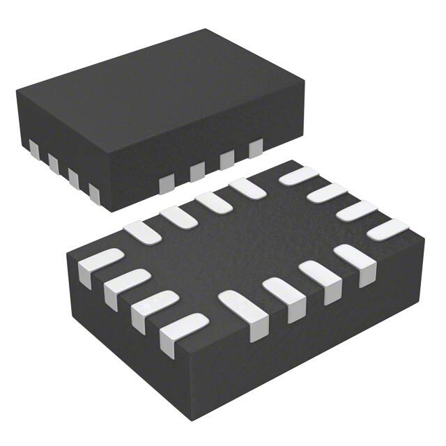
• Compact miniQFN16 package
(1.8 mm x 2.6 mm x 0.55 mm)
The DG9454E is designed to operate from a 3 V to 16 V
supply at V+, and 2.5 V to 5.5 V at VL, while guarantees
1.8 V logic compatible over the full operation voltage range.
Processed with advanced CMOS technology, the DG9454E
conducts equally well in both directions, offers rail to rail
analog signal handling and can be used both as a
multiplexer as well as a de-multiplexer.
• Material categorization: for definitions of
compliance please see www.vishay.com/doc?99912
APPLICATIONS
The DG9454E operating temperature is specified
from -40 °C to +125 °C. It is available in ultra-compact
1.8 mm x 2.6 mm miniQFN16 package of lead (Pb)-free
nickel-palladium-gold device termination. It is represented
by the lead (Pb)-free “-E4” suffix. The nickel-palladium-gold
device terminations meet all JEDEC® standards for reflow
and MSL ratings.
•
•
•
•
•
•
•
•
Medical and healthcare systems
Data acquisition systems
Meters and instruments
Games and Goggles
Automatic test equipment
Process control and automation
Communication systems
Battery powered systems
BENEFITS
•
•
•
•
•
•
Low power consumption
Precision switching
Low voltage logic interface
Bi-directional rail to rail signal switching
Compact package option
Extended operation temperature range
FUNCTIONAL BLOCK DIAGRAM AND PIN CONFIGURATION
DG9454E
mQFN-16
Y0
Y1
V+
Y
16
15
14
13
Z1
1
12
X
Z
2
11
X1
Z0
3
10
X0
Enable
4
9
A
Yxx
Pin 1
5
6
77
8
VL
GND
C
B
Device Marking: Jxx for DG9454E
(miniQFN16)
xx = Date/Lot Traceability Code
Top View
S16-0652-Rev. A, 18-Apr-16
Document Number: 67172
1
For technical questions, contact: analogswitchtechsupport@vishay.com
THIS DOCUMENT IS SUBJECT TO CHANGE WITHOUT NOTICE. THE PRODUCTS DESCRIBED HEREIN AND THIS DOCUMENT
ARE SUBJECT TO SPECIFIC DISCLAIMERS, SET FORTH AT www.vishay.com/doc?91000
�DG9454E
www.vishay.com
Vishay Siliconix
TRUTH TABLE
SELECT INPUTS
ON SWITCHES
ENABLE
INPUT
C
B
A
DG9454E
H
X
X
X
All Switches Open
L
L
L
L
X to X0, Y to Y0, Z to Z0
L
L
L
H
X to X1, Y to Y0, Z to Z0
L
L
H
L
X to X0, Y to Y1, Z to Z0
L
L
H
H
X to X1, Y to Y1, Z to Z0
L
H
L
L
X to X0, Y to Y0, Z to Z1
L
H
L
H
X to X1, Y to Y0, Z to Z1
L
H
H
L
X to X0, Y to Y1, Z to Z1
L
H
H
H
X to X1, Y to Y1, Z to Z1
ORDERING INFORMATION
TEMP. RANGE
-40 °C to +85 °C lead (Pb)-free
PACKAGE
PART NUMBER
MIN. ORDER / PACK. QUANTITY
16-Pin miniQFN
DG9454EEN-T1-GE4
Tape and reel, 3000 units
ABSOLUTE MAXIMUM RATINGS (TA = 25 °C, unless otherwise noted)
PARAMETER
Digital Inputs
a,
VS, VD, VL
V+ to GND
LIMIT
UNIT
GND - 0.3 to (V+) + 0.3
or 30 mA, whichever occurs first
V
-0.3 to +18
Continuous Current (any terminal)
30
Peak Current, S or D (pulsed 1 ms, 10 % duty cycle)
100
Storage Temperature
Power Dissipation b
Thermal Resistance b
mA
-65 to +150
°C
16-Pin miniQFN c, d
525
mW
16-Pin miniQFN d
152
°C/W
Latch-Up (per JESD78)
100
mA
ESD Human Body Model (HBM); per ANSI / ESDA / JEDEC JS-001
2500
V
Notes
a. Signals on SX, DX, VL or INX exceeding V+ will be clamped by internal diodes. Limit forward diode current to maximum current ratings.
b. All leads welded or soldered to PC board.
c. Derate 6.6 mW/°C above 70 °C.
d. Manual soldering with iron is not recommended for leadless components. The miniQFN-16 is a leadless package. The end of the lead
terminal is exposed copper (not plated) as a result of the singulation process in manufacturing. A solder fillet at the exposed copper lip
cannot be guaranteed and is not required to ensure adequate bottom side solder interconnection.
Stresses beyond those listed under “Absolute Maximum Ratings” may cause permanent damage to the device. These are stress ratings only, and functional operation
of the device at these or any other conditions beyond those indicated in the operational sections of the specifications is not implied. Exposure to absolute maximum
rating conditions for extended periods may affect device reliability.
S16-0652-Rev. A, 18-Apr-16
Document Number: 67172
2
For technical questions, contact: analogswitchtechsupport@vishay.com
THIS DOCUMENT IS SUBJECT TO CHANGE WITHOUT NOTICE. THE PRODUCTS DESCRIBED HEREIN AND THIS DOCUMENT
ARE SUBJECT TO SPECIFIC DISCLAIMERS, SET FORTH AT www.vishay.com/doc?91000
�DG9454E
www.vishay.com
Vishay Siliconix
SPECIFICATIONS FOR UNIPOLAR SUPPLIES
-40 °C to +125 °C -40 °C to +85 °C
TEST CONDITIONS
UNLESS OTHERWISE SPECIFIED
b
c
SYMBOL
TEMP. TYP.
V+ = 12 V, VL = 2.7 V
MIN. d MAX. d MIN. d MAX. d
VIN(A, B, C and enable) = 1.8 V, 0.5 V a
PARAMETER
UNIT
Analog Switch
Analog Signal Range e
VANALOG
On-Resistance
RON
RON
IS = 1 mA, VD = 0.7 V, 11.3 V
RFLATNESS
IS = 1 mA, VD = 0.7 V, 6 V, 11.3 V
On-Resistance Match
On-Resistance Flatness
IS = 1 mA, VD = 0.7 V, 6 V, 11.3 V
IS(off)
Switch Off
Leakage Current
ID(off)
Channel On
Leakage Current
ID(on)
V+ = 13.2 V, VL = 2.7 V
VD = 1 V / 12.2 V, VS = 12.2 V / 1 V
V+ = 13.2 V, VL = 2.7 V
VD = VS = 1 V / 12.2 V
Full
-
0
12
0
12
Room
85
-
103
-
103
125
Full
-
-
133
-
Room
1.24
-
8
-
8
Full
-
-
8
-
8
Room
27
-
37
-
37
Full
-
-
44
-
43
Room
± 0.05
-1
1
-1
1
Full
-
-50
50
-5
5
Room
± 0.07
-1
1
-1
1
Full
-
-50
50
-5
5
Room
± 0.07
-1
1
-1
1
Full
-
-50
50
-5
5
V
nA
Digital Control
Logic Low Input Voltage
VINL
Logic High Input Voltage
VINH
Logic Low Input Current
IL
Logic High Input current
IH
Full
-
-
0.5
-
0.5
Full
-
1.8
-
1.8
-
VIN(A0, A1, A2 and enable)
under test = 0.5 V
Full
0.02
-1
1
-1
1
VIN(A0, A1, A2 and enable)
under test = 1.8 V
Full
0.02
-1
1
-1
1
Room
79
-
119
-
119
Full
-
-
134
-
126
Room
70
-
110
-
110
Full
-
-
130
-
116
Room
51
-
91
-
91
Full
-
-
95
-
94
Room
17
-
-
-
-
Full
-
1
-
1
-
Full
5.84
-
-
-
-
100 kHz
Room
-95
-
-
-
-
VL = 2.7 V
V
μA
Dynamic Characteristics
Transition Time
tTRANS
Enable Turn-On Time
tON(EN)
Enable Turn-Off Time
tOFF(EN)
Break-Before-Make
Time Delay
tD
Charge Injection e
Q
Off Isolation e
RL = 300 , CL = 35 pF
see Fig. 1, 2, 3
CL = 1 nF, RGEN = 0 , VGEN = 0 V
OIRR
f = 1 MHz,
RL = 50 , CL = 5 pF
Crosstalk e
Bandwidth, -3 dB
XTALK
e
BW
Source Off Capacitance e
CS(off)
Drain Off Capacitance e
CD(off)
Channel On Capacitance e
CD(on)
Total Harmonic
Distortion e
THD
S16-0652-Rev. A, 18-Apr-16
1 MHz
Room
-85
-
-
-
-
10 MHz
Room
-65
-
-
-
-
100 kHz
Room
-92
-
-
-
-
1 MHz
Room
-73
-
-
-
-
10 MHz
Room
-53
-
-
-
-
Room
356
-
-
-
-
Room
3.1
-
-
-
-
Room
4
-
-
-
-
Room
8.8
-
-
-
-
Room
0.075
-
-
-
-
RL = 50
f = 1 MHz
Signal = 1 VRMS,
20 Hz to 20 kHz, RL = 600
ns
pC
dB
MHz
pF
%
Document Number: 67172
3
For technical questions, contact: analogswitchtechsupport@vishay.com
THIS DOCUMENT IS SUBJECT TO CHANGE WITHOUT NOTICE. THE PRODUCTS DESCRIBED HEREIN AND THIS DOCUMENT
ARE SUBJECT TO SPECIFIC DISCLAIMERS, SET FORTH AT www.vishay.com/doc?91000
�DG9454E
www.vishay.com
Vishay Siliconix
SPECIFICATIONS FOR UNIPOLAR SUPPLIES
PARAMETER
SYMBOL
-40 °C to +125 °C -40 °C to +85 °C
TEST CONDITIONS
UNLESS OTHERWISE SPECIFIED
TEMP. b TYP. c
V+ = 12 V, VL = 2.7 V
MIN. d MAX. d MIN. d MAX. d
VIN(A, B, C and enable) = 1.8 V, 0.5 V a
UNIT
Power Supply
Power Supply Range
I+
VIN(A, B, C and enable) = 0 V or 12 V
Ground Current
Logic Supply Current
IGND
IL
VL = 2.7 V
Room
0.05
-
1
-
1
Full
-
-
10
-
10
Room
0.05
-1
-
-1
-
Full
-
-10
-
-10
-
Room
0.05
-
1
-
1
Full
-
-
10
-
10
μA
Notes
a. VIN = input voltage to perform proper function.
b. Room = 25 °C, Full = as determined by the operating temperature suffix.
c. Typical values are for DESIGN AID ONLY, not guaranteed nor subject to production testing.
d. The algebraic convention whereby the most negative value is a minimum and the most positive a maximum, is used in this datasheet.
e. Guaranteed by design, not subject to production test.
S16-0652-Rev. A, 18-Apr-16
Document Number: 67172
4
For technical questions, contact: analogswitchtechsupport@vishay.com
THIS DOCUMENT IS SUBJECT TO CHANGE WITHOUT NOTICE. THE PRODUCTS DESCRIBED HEREIN AND THIS DOCUMENT
ARE SUBJECT TO SPECIFIC DISCLAIMERS, SET FORTH AT www.vishay.com/doc?91000
�DG9454E
www.vishay.com
Vishay Siliconix
SPECIFICATIONS FOR UNIPOLAR SUPPLIES
PARAMETER
SYMBOL
-40 °C to +125 °C -40 °C to +85 °C
TEST CONDITIONS
UNLESS OTHERWISE SPECIFIED
UNIT
TEMP. b TYP. c
V+ = 5 V, VL = 2.7 V
MIN. d MAX. d MIN. d MAX. d
VIN(A, B, C and enable) = 1.8 V, 0.5 V a
Analog Switch
Analog Signal Range e
On-Resistance
On-Resistance Match
On-Resistance Flatness
Switch Off
Leakage Current
VANALOG
RON
RON
IS = 1 mA, VD = 3.5 V
RFLATNESS
IS = 1 mA, VD = 0 V, 3 V
IS(off)
ID(off)
Channel On
Leakage Current
IS = 1 mA, VD = 0 V, 3.5 V
V+ = 5.5 V, V- = 0 V
VD = 1 V / 4.5 V, VS = 4.5 V / 1 V
Full
-
0
5
0
5
Room
125
-
147
-
147
Full
-
-
176
-
168
Room
1.33
-
8
-
8
Full
-
-
8
-
8
Room
21
-
31
-
31
Full
-
-
25
-
29
Room
± 0.03
-1
1
-1
1
Full
-
-50
50
-5
5
Room
± 0.03
-1
1
-1
1
Full
-
-50
50
-5
5
ID(on)
V+ = 5.5 V, V- = 0 V
VD = VS = 1 V / 4.5 V
Room
± 0.03
-1
1
-1
1
Full
-
-50
50
-5
5
VIN(A, B, C and enable) Low
VIL
VL = 2.7 V
Full
-
-
0.6
-
0.6
VIN(A, B, C and enable) High
VIH
VL = 2.7 V
Full
-
1.8
-
1.8
-
Input Current, VIN Low
IL
VIN(A, B, C and enable) under test = 0.6 V
Full
0.02
-1
1
-1
1
Input Current, VIN High
IH
VIN(A, B, C and enable) under test = 1.8 V
Full
0.02
-1
1
-1
1
Room
95
-
135
-
135
Full
-
-
164
-
152
Room
80
-
120
-
120
V
nA
Digital Control
V
μA
Dynamic Characteristics
Transition Time
Enable Turn-On Time
Enable Turn-Off Time
tTRANS
tON
RL = 300 , CL = 35 pF
see Fig. 1, 2, 3
tOFF
Break-Before-Make
Time Delay
tD
Charge Injection e
Q
Off Isolation e
OIRR
Channel-to-Channel
Crosstalk e
XTALK
Source Off Capacitance e
CS(off)
Drain Off Capacitance e
CD(off)
Channel On Capacitance e
CD(on)
Full
-
-
138
-
129
Room
58
-
98
-
98
Full
-
-
106
-
103
Room
45
-
-
-
-
Full
-
24
-
15
-
Vg = 0 V, Rg = 0 , CL = 1 nF
Full
1.44
-
-
-
-
RL = 50 , CL = 5 pF
f = 100 kHz
Room
-95
-
-
-
-
Room
-92
-
-
-
-
Room
3.5
-
-
-
-
Room
4.5
-
-
-
-
Room
10.2
-
-
-
-
Room
0.05
-
1
-
1
Full
-
-
10
-
10
Room
-0.05
-1
-
-1
-
Full
-
-10
-
-10
-
Room
0.05
-
1
-
1
Full
-
-
10
-
10
f = 1 MHz
ns
pC
dB
pF
Power Supply
Power Supply Current
I+
VIN(A, B, C and enable) = 0 V or 5 V
Ground Current
Logic Supply Current
IGND
IL
VL = 2.7 V
μA
Notes
a. VIN = input voltage to perform proper function.
b. Room = 25 °C, Full = as determined by the operating temperature suffix.
c. Typical values are for DESIGN AID ONLY, not guaranteed nor subject to production testing.
d. The algebraic convention whereby the most negative value is a minimum and the most positive a maximum, is used in this datasheet.
e. Guaranteed by design, not subject to production test.
S16-0652-Rev. A, 18-Apr-16
Document Number: 67172
5
For technical questions, contact: analogswitchtechsupport@vishay.com
THIS DOCUMENT IS SUBJECT TO CHANGE WITHOUT NOTICE. THE PRODUCTS DESCRIBED HEREIN AND THIS DOCUMENT
ARE SUBJECT TO SPECIFIC DISCLAIMERS, SET FORTH AT www.vishay.com/doc?91000
�DG9454E
www.vishay.com
Vishay Siliconix
SPECIFICATIONS FOR UNIPOLAR SUPPLIES
PARAMETER
-40 °C to +125 °C -40 °C to +85 °C
TEST CONDITIONS
UNLESS OTHERWISE SPECIFIED
b
c
UNIT
SYMBOL
TEMP. TYP.
V+ = 3 V, VL = 2.7 V
MIN. d MAX. d MIN. d MAX. d
VIN(A, B, C AND ENABLE) = 1.5 V, 0.6 V a
Analog Switch
Analog Signal Range e
On-Resistance
Switch Off
Leakage Current
VANALOG
RON
IS(off)
ID(off)
Channel On
Leakage Current
ID(on)
IS = 1 mA, VD = 1.5 V
V+ = 3.3 V, VL = 2.7 V
VD = 0.3 V / 3 V, VS = 3 V / 0.3 V
V+ = 3.3 V, VL = 2.7 V
VS = VD = 0.3 V / 3 V
Full
-
0
3
0
3
V
Room
221
-
-
-
-
Full
-
-
-
-
-
Room
± 0.02
-1
1
-1
1
Full
-
-50
50
-5
5
Room
± 0.02
-1
1
-1
1
Full
-
-50
50
-5
5
Room
± 0.02
-1
1
-1
1
Full
-
-50
50
-5
5
nA
Digital Control
Logic Low Input Voltage
VINL
Logic High Input Voltage
VINH
Logic Low Input Current
IL
Logic High Input Current
IH
Full
-
-
0.6
-
0.6
Full
-
1.8
-
1.8
-
VIN(A0, A1, A2 and enable)
under test = 0.6 V
Full
0.02
-1
1
-1
1
VIN(A0, A1, A2 and enable)
under test = 1.8 V
Full
0.02
-1
1
-1
1
Room
161
-
-
-
-
Full
-
-
-
-
-
Room
120
-
-
-
-
Full
-
-
-
-
-
Room
79
-
-
-
-
VL = 2.7 V
V
μA
Dynamic Characteristics
Transition Time
tTRANS
Enable Turn-On Time
tON(EN)
Enable Turn-Off Time
tOFF(EN)
Break-Before-Make
Time Delay
Charge Injection e
RL = 300 , CL = 35 pF
see Fig. 1, 2, 3
tD
Q
Off Isolation e
OIRR
Crosstalk e
XTALK
Source Off Capacitance e
CS(off)
Drain Off Capacitance e
CD(off)
Channel On Capacitance e
CD(on)
CL = 1 nF, RGEN = 0 , VGEN = 0 V
f = 1 MHz, RL = 50 ,
CL = 5 pF
Full
-
-
-
-
Room
98
-
-
-
-
Full
-
-
-
-
-
Full
0.58
-
-
-
-
100 kHz
Room
-95
-
-
-
-
100 kHz
Room
-92
-
-
-
-
f = 1 MHz
Room
3.7
-
-
-
-
Room
4.7
-
-
-
-
Room
10.4
-
-
-
-
Room
0.05
-
1
-
1
Full
-
-
10
-
10
Room
0.05
-1
-
-1
-
Full
-
-10
-
-10
-
Room
0.05
-
1
-
1
Full
-
-
10
-
10
ns
pC
dB
pF
Power Supply
Power Supply Range
I+
VIN (A, B, C and enable) = 0 V or 3 V
Ground Current
Logic Supply Current
IGND
IL
VL = 2.7 V
μA
Notes
a. VIN = input voltage to perform proper function.
b. Room = 25 °C, Full = as determined by the operating temperature suffix.
c. Typical values are for DESIGN AID ONLY, not guaranteed nor subject to production testing.
d. The algebraic convention whereby the most negative value is a minimum and the most positive a maximum, is used in this datasheet.
e. Guaranteed by design, not subject to production test.
S16-0652-Rev. A, 18-Apr-16
Document Number: 67172
6
For technical questions, contact: analogswitchtechsupport@vishay.com
THIS DOCUMENT IS SUBJECT TO CHANGE WITHOUT NOTICE. THE PRODUCTS DESCRIBED HEREIN AND THIS DOCUMENT
ARE SUBJECT TO SPECIFIC DISCLAIMERS, SET FORTH AT www.vishay.com/doc?91000
�DG9454E
www.vishay.com
Vishay Siliconix
TYPICAL CHARACTERISTICS (25 °C, unless otherwise noted)
225
400
V+ = +3 V, V- = 0 V
350
175
RON - On-Resistance (Ω)
RON - On-Resistance (Ω)
300
V+ = +5 V, V- = 0 V
250
200
150
V+ = +12 V, V - = 0 V
V+ = +16 V, V - = 0 V
100
+125 °C
+85 °C
150
125
100
75
25
0
0
0
2
4
6
8
10
12
14
16
0.0
18
0.5
1.0
1.5
2.5
3.0
3.5
4.0
4.5
5.0
VD - Analog Voltage (V)
On-Resistance vs. VD and Signal Supply Voltage
On-Resistance vs. Analog Voltage and Temperature
175
V+ = +12 V
v- = 0 V
IS = 1 mA
V+ = +3 V, V- = 0 V, tON
100
+125 °C
+85 °C
80
60
40
+25 °C
20
-40 °C
150
tON(EN), tOFF(EN) - Switching Time (ns)
120
V+ = +5 V, V- = 0 V, tON
125
V+ = +3 V, V- = 0 V, tOFF
0
1
2
3
4
5
6
7
8
9
V+ = +12 V, V- = 0 V, tON
100
V+ = +16 V, V- = 0 V, tON
75
50
V+ = +5 V, V- = 0 V, tOFF
25
0
V+ = +12 V, V- = 0 V, tOFF
V+ = +16 V, V- = 0 V, tOFF
0
10 11 12
-60 -40
-20
VD - Analog Voltage (V)
0
20 40 60 80
Temperature (°C)
100 120 140
Switching Time vs. Temperature
On-Resistance vs. Analog Voltage and Temperature
100n
0
-10
V+ = +13.2 V
V- = -0 V
ID(ON), VD = 12.2 V
Loss
-20
Loss, OIRR, XTALK (dB)
Leakage Current (A)
2.0
VD - Analog Voltage (V)
140
10n
-40 °C
+25 °C
50
50
RON - On-Resistance (Ω)
V+ = +5 V
v- = 0 V
IS = 1 mA
200
TA = 25 °C
IS = -1 mA
ID(OFF), VD = 12.2 V, VS = 1 V
1n
IS(OFF), VD = 12.2 V, VS = 1 V
100p
10p
-30
-40
XTALK
-50
OIRR
-60
-70
V+ = 12 V
VL = 2.7 V
RL = 50 Ω
-80
-90
1p
-60 -40 -20
0
20
40
60
80
100 120 140
-100
100K
Temperature (°C)
10M
Frequency (Hz)
Leakage Current vs. Temperature
Insertion Loss, Off-Isolation, Crosstalk vs. Frequency
S16-0652-Rev. A, 18-Apr-16
1M
100M
1G
Document Number: 67172
7
For technical questions, contact: analogswitchtechsupport@vishay.com
THIS DOCUMENT IS SUBJECT TO CHANGE WITHOUT NOTICE. THE PRODUCTS DESCRIBED HEREIN AND THIS DOCUMENT
ARE SUBJECT TO SPECIFIC DISCLAIMERS, SET FORTH AT www.vishay.com/doc?91000
�DG9454E
www.vishay.com
Vishay Siliconix
1.6
1.5
1.4
1.3
1.2
1.1
1.0
0.9
0.8
0.7
0.6
0.5
0.4
0.3
0.2
0.1
0
8.0
-40 °C to +125 °C
6.0
V+ = 5 V
QINJ - Charge Injection (pC)
VT - Switching Threshold (V)
TYPICAL CHARACTERISTICS (25 °C, unless otherwise noted)
VIH = -40 °C
VIL = 125 °C
V+ = 12 V
4.0
V+ = 3 V
2.0
0
-2.0
-4.0
-6.0
VL = 2.7 V
-8.0
-10.0
0
2
4
6
8
10 12 14
V+ - Supply Voltage (V)
16
18
20
0
Switching Threshold vs. Logic Supply Voltage
1
2
3
4
5
6
7
8
9
VS - Analog Voltage (V)
10 11 12
Charge Injection vs. Analog Voltage
100m
IL - Supply Current (μA)
10m
V+ = 12V
VL = 2.7 V
T = 25 °C
1m
100n
10n
1n
100p
10p
1p
0
1
2
3
4
5
6
7
8
9
10 11 12
VIN (V)
IL vs. VIN
SCHEMATIC DIAGRAM (typical channel)
V+
VL
X, Y, Z
A, B
VBody
snatcher
GND
Level
shift
C
V+
V-
Decode/
drive
X0, Y0, Z0
VEN
X1, Y1, Z1
V-
V-
S16-0652-Rev. A, 18-Apr-16
Document Number: 67172
8
For technical questions, contact: analogswitchtechsupport@vishay.com
THIS DOCUMENT IS SUBJECT TO CHANGE WITHOUT NOTICE. THE PRODUCTS DESCRIBED HEREIN AND THIS DOCUMENT
ARE SUBJECT TO SPECIFIC DISCLAIMERS, SET FORTH AT www.vishay.com/doc?91000
�DG9454E
www.vishay.com
Vishay Siliconix
TEST CIRCUITS
V+
1.8 V
50 %
VA, B, C
X0 or Y0
or Z0
A or B
or C
VX0 or VY0 or VZ0
VX0 or VY0 or VZ0
50 Ω
90 %
DG9454E
X1 or Y1 or Z1
VO
GND
50 %
VX1 or VY1 or VZ1
VO
X or Y or Z
ENABLE
0V
300 Ω
VX1
VX7
VX3 or VY3
or VY1 or VZ1
90 %
t TRANS
35 pF
t TRANS
V0 or Y0 or Z0 ON
X1 or Y1 or Z1 ON (DG9454)
VL
Fig. 1 - Transition Time
V+
1.8 V
VENABLE
X0 or Y0
or Z0
A or B
or C
V+
VX0 or VY0 or VZ0
X1 or Y1 or Z1
DG9454E
50 Ω
GND
90 %
VO
50 %
VO
X or Y or Z
ENABLE
50 %
0V
300 Ω
90 %
0V
35 pF
t OFF
tON
Disable X or Y or Z
Enable X or Y or Z
VL
Fig. 2 - Enable Switching Time
V+
1.8 V
VA, B, C
A or B
or C
X0, X1 or Y0,
Y1 or Z0, Z1
50 %
0V
V+
50 Ω
VX0 or VY0 or VZ0
80 %
DG9454E
ENABLE
VO
VO
X or Y or Z
GND
300 Ω
35 pF
0V
tD
VL
Fig. 3 - Break-Before-Make
S16-0652-Rev. A, 18-Apr-16
Document Number: 67172
9
For technical questions, contact: analogswitchtechsupport@vishay.com
THIS DOCUMENT IS SUBJECT TO CHANGE WITHOUT NOTICE. THE PRODUCTS DESCRIBED HEREIN AND THIS DOCUMENT
ARE SUBJECT TO SPECIFIC DISCLAIMERS, SET FORTH AT www.vishay.com/doc?91000
�DG9454E
www.vishay.com
Vishay Siliconix
TEST CIRCUITS
V+
tr < 5 ns
tf < 5 ns
V+
A
B
C
Channel
Select
ON
OFF
VENABLE
OFF
0V
Rg
Xx
VO
Vg
ΔVO
VO
X
ENABLE
GND
1 nF
VL
Fig. 4 - Charge Injection
V+
V+
Network Analyzer
Network Analyzer
VIN
A
B
C
X0
VOUT
X
ENABLE
A
B
C
Rg = 50 Ω
Vg
V+
GND
VIN
X0
Vg
VOUT
X
ENABLE
GND
50 Ω
Rg = 50 Ω
50 Ω
VL
VL
Insertion Loss = 20 log
VOUT
VIN
Off Isolation = 20 log
VOUT
VIN
Fig. 7 - Off Isolation
Fig. 5 - Insertion Loss
V+
V+
Network Analyzer
A
B
C
X0
VIN
Vg
Rg = 50 Ω
Channel
Select
A
B
C
X0
|
to
|
Xx
X
50 Ω
Xx
ENABLE
VOUT
GND
50 Ω
ENABLE
Impedance
Analyzer
X
GND
VL
Crosstalk = 20 log
VOUT
VIN
Fig. 6 - Crosstalk
VL
Fig. 8 - Source, Drain Capacitance
Vishay Siliconix maintains worldwide manufacturing capability. Products may be manufactured at one of several qualified locations. Reliability data for Silicon
Technology and Package Reliability represent a composite of all qualified locations. For related documents such as package/tape drawings, part marking, and
reliability data, see www.vishay.com/ppg?67172.
S16-0652-Rev. A, 18-Apr-16
Document Number: 67172
10
For technical questions, contact: analogswitchtechsupport@vishay.com
THIS DOCUMENT IS SUBJECT TO CHANGE WITHOUT NOTICE. THE PRODUCTS DESCRIBED HEREIN AND THIS DOCUMENT
ARE SUBJECT TO SPECIFIC DISCLAIMERS, SET FORTH AT www.vishay.com/doc?91000
�Package Information
www.vishay.com
Vishay Siliconix
Thin miniQFN16 Case Outline
B
12
0.10 C
Terminal tip (4)
16 x b
D
A
11
9
9
10
10
11
0.10 M C A B
0.05 M C
12
13
8
8
13
14
7
7
14
6
6
15
5
5
E
15
16
1
2
3
4
16
4
Pin #1 identifier (5)
15 x L
0.10 C
Top view
3
2
L1
1
e
Bottom view
0.10 C
C
A
Seating
plane
0.10 C
A3
Side view
DIMENSIONS
MILLIMETERS (1)
INCHES
MIN.
NOM.
MAX.
MIN.
NOM.
MAX.
A
0.50
0.55
0.60
0.020
0.022
0.024
A1
0
-
0.05
0
-
0.002
A3
0.15 ref.
b
0.15
D
2.50
e
0.006 ref.
0.20
0.25
0.006
2.60
2.70
0.098
0.40 BSC
E
1.70
1.80
0.008
0.010
0.102
0.106
0.016 BSC
1.90
0.067
0.071
0.075
L
0.35
0.40
0.45
0.014
0.016
0.018
L1
0.45
0.50
0.55
0.018
0.020
0.022
N (3)
16
16
Nd (3)
4
4
(3)
4
4
Ne
Notes
(1) Use millimeters as the primary measurement.
(2) Dimensioning and tolerances conform to ASME Y14.5M. - 1994.
(3) N is the number of terminals. Nd and Ne is the number of terminals in each D and E site respectively.
(4) Dimensions b applies to plated terminal and is measured between 0.15 mm and 0.30 mm from terminal tip.
(5) The pin 1 identifier must be existed on the top surface of the package by using identification mark or other feature of package body.
(6) Package warpage max. 0.05 mm.
ECN: T16-0226-Rev. B, 09-May-16
DWG: 6023
Revision: 09-May-16
Document Number: 64694
1
For technical questions, contact: analogswitchtechsupport@vishay.com
THIS DOCUMENT IS SUBJECT TO CHANGE WITHOUT NOTICE. THE PRODUCTS DESCRIBED HEREIN AND THIS DOCUMENT
ARE SUBJECT TO SPECIFIC DISCLAIMERS, SET FORTH AT www.vishay.com/doc?91000
�PAD Pattern
Vishay Siliconix
RECOMMENDED MINIMUM PADS FOR MINI QFN 16L
0.562
(0.0221)
0.400
(0.0157)
0.225
(0.0089)
1
2.900
(0.1142)
0.463
(0.0182)
1.200
(0.0472)
2.100
(0.0827)
Mounting Footprint
Dimensions in mm (inch)
Document Number: 66557
Revision: 05-Mar-10
www.vishay.com
1
�Legal Disclaimer Notice
www.vishay.com
Vishay
Disclaimer
ALL PRODUCT, PRODUCT SPECIFICATIONS AND DATA ARE SUBJECT TO CHANGE WITHOUT NOTICE TO IMPROVE
RELIABILITY, FUNCTION OR DESIGN OR OTHERWISE.
Vishay Intertechnology, Inc., its affiliates, agents, and employees, and all persons acting on its or their behalf (collectively,
“Vishay”), disclaim any and all liability for any errors, inaccuracies or incompleteness contained in any datasheet or in any other
disclosure relating to any product.
Vishay makes no warranty, representation or guarantee regarding the suitability of the products for any particular purpose or
the continuing production of any product. To the maximum extent permitted by applicable law, Vishay disclaims (i) any and all
liability arising out of the application or use of any product, (ii) any and all liability, including without limitation special,
consequential or incidental damages, and (iii) any and all implied warranties, including warranties of fitness for particular
purpose, non-infringement and merchantability.
Statements regarding the suitability of products for certain types of applications are based on Vishay’s knowledge of
typical requirements that are often placed on Vishay products in generic applications. Such statements are not binding
statements about the suitability of products for a particular application. It is the customer’s responsibility to validate that a
particular product with the properties described in the product specification is suitable for use in a particular application.
Parameters provided in datasheets and / or specifications may vary in different applications and performance may vary over
time. All operating parameters, including typical parameters, must be validated for each customer application by the customer’s
technical experts. Product specifications do not expand or otherwise modify Vishay’s terms and conditions of purchase,
including but not limited to the warranty expressed therein.
Except as expressly indicated in writing, Vishay products are not designed for use in medical, life-saving, or life-sustaining
applications or for any other application in which the failure of the Vishay product could result in personal injury or death.
Customers using or selling Vishay products not expressly indicated for use in such applications do so at their own risk.
Please contact authorized Vishay personnel to obtain written terms and conditions regarding products designed for
such applications.
No license, express or implied, by estoppel or otherwise, to any intellectual property rights is granted by this document
or by any conduct of Vishay. Product names and markings noted herein may be trademarks of their respective owners.
© 2017 VISHAY INTERTECHNOLOGY, INC. ALL RIGHTS RESERVED
Revision: 08-Feb-17
1
Document Number: 91000
�


 工商网监
湘ICP备2023018690号
工商网监
湘ICP备2023018690号

