Si1865DDL
www.vishay.com
Vishay Siliconix
Load Switch with Level-Shift
FEATURES
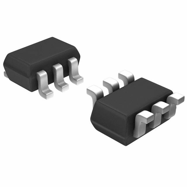
SOT-363
SC-70 (6 leads)
ON/OFF
5
R1, C1
6
• Low RDS(on) TrenchFET®
• 1.8 V to 12 V input
S2
4
• 1.5 V to 8 V logic level control
• Low profile, small footprint SC-70-6 package
• 2000 V ESD protection on input switch, VON/OFF
• Adjustable slew-rate
1
R2
Top View
3
D2
2
D2
• Material categorization: for definitions of compliance
please see www.vishay.com/doc?99912
APPLICATIONS
• Load switch with level-shift
Marking Code: VD
• Slew-rate control
• Portable / consumer devices
PRODUCT SUMMARY
VDS (V)
12
RDS(on) () at VIN = 4.5 V
0.200
RDS(on) () at VIN = 2.5 V
0.300
RDS(on) () at VIN = 1.8 V
0.508
ID (A)
DESCRIPTION
The Si1865DDL includes a p- and n-channel MOSFET in
a single SC-70-6 package. The low on-resistance p-channel
TrenchFET is tailored for use as a load switch. The
n-channel, with an external resistor, can be used as a
level-shift to drive the p-channel load-switch. The n-channel
MOSFET has internal ESD protection and can be driven by
logic signals as low as 1.5 V. The Si1865DDL operates on
supply lines from 1.8 V to 12 V, and can drive loads up to
1.1 A.
± 1.1
Configuration
Level-shift
APPLICATION CIRCUITS
Si1865DDL
2, 3
4
14
VOUT
VIN
IL = 1 A
VON/OFF = 3 V
Ci = 10 µF
Co = 1 µF
Q2
R1
C1
6
6
10.5
tr
5
ON/OFF
Co
LOAD
Time (us)
tf
7
Q1
td(off)
3.5
Ci
td(on)
1
0
R2
0
GND
R2
2
4
6
8
10
R2 (kΩ)
Switching Variation R2 at VIN = 2.5 V, R1 = 20 k
COMPONENTS
R1
Pull-up resistor
Typical 10 k to 1 M a
R2
Optional slew-rate control
Typical 0 to 100 k a
C1
Optional slew-rate control
Typical 1000 pF
Note
a. Minimum R1 value should be at least 10 x R2 to ensure Q1
turn-on
S13-2618-Rev. B, 23-Dec-13
The Si1865DDL is ideally suited for high-side load switching
in portable applications. The integrated n-channel level-shift
device saves space by reducing external components. The
slew rate is set externally so that rise-times can be tailored
to different load types.
Document Number: 62888
1
For technical questions, contact: pmostechsupport@vishay.com
THIS DOCUMENT IS SUBJECT TO CHANGE WITHOUT NOTICE. THE PRODUCTS DESCRIBED HEREIN AND THIS DOCUMENT
ARE SUBJECT TO SPECIFIC DISCLAIMERS, SET FORTH AT www.vishay.com/doc?91000
�Si1865DDL
www.vishay.com
Vishay Siliconix
FUNCTIONAL BLOCK DIAGRAM
Si1865DDL
4
2, 3
S2
D2
Q2
6
R1, C1
Q1
5
ON/OFF
1
R2
ORDERING INFORMATION
Package
SC-70
Lead (Pb)-free and halogen-free
Si1865DDL-T1-GE3
ABSOLUTE MAXIMUM RATINGS (TA = 25 °C, unless otherwise noted)
PARAMETER
SYMBOL
LIMIT
Input voltage
VIN(VDS2)
12
On/off voltage
VON/OFF
8
Continuous a, b
Load current
Continuous intrinsic diode conduction a
Operating junction and storage temperature range
ESD rating, MIL-STD-883D human body model (100 pF, 1500 )
A
±5
IS
Maximum power dissipation a
V
± 1.1
IL
Pulsed b, c
UNIT
-0.3
PD
0.357
W
TJ, Tstg
-55 to 150
°C
ESD
2
kV
THERMAL RESISTANCE RATINGS
PARAMETER
SYMBOL
TYPICAL
MAXIMUM
Maximum junction-to-ambient (continuous current) a
RthJA
290
350
Maximum junction-to-foot (Q2)
RthJF
250
300
UNIT
°C/W
SPECIFICATIONS (TJ = 25 °C, unless otherwise noted)
PARAMETER
SYMBOL
TEST CONDITIONS
MIN.
Reverse leakage current
IFL
VIN = 12 V, VON/OFF = 0 V
-
Diode forward voltage
VSD
IS = -0.8 A
-
TYP.
MAX.
UNIT
-
1
μA
-0.84
-1.2
V
V
Off Characteristics
On Characteristics
Input voltage range
On-resistance (p-channel)
On-state (p-channel) drain-current
VIN
RDS(on)
ID(on)
1.8
-
12
VON/OFF = 1.5 V, VIN = 4.5 V, ID = 1.1 A
-
0.165
0.200
VON/OFF = 1.5 V, VIN = 2.5 V, ID = 0.9 A
-
0.250
0.300
VON/OFF = 1.5 V, VIN = 1.8 V, ID = 0.2 A
-
0.376
0.508
VIN-OUT 0.2 V, VIN = 5 V, VON/OFF = 1.5 V
1
-
-
VIN-OUT 0.3 V, VIN = 3 V, VON/OFF = 1.5 V
1
-
-
A
Notes
a. Surface mounted on FR4 board
b. VIN = 12 V, VON/OFF = 8 V, TA = 25 °C
c. Pulse test: pulse width 300 μs, duty cycle 2 %
Stresses beyond those listed under “Absolute Maximum Ratings” may cause permanent damage to the device. These are stress ratings only, and functional operation
of the device at these or any other conditions beyond those indicated in the operational sections of the specifications is not implied. Exposure to absolute maximum
rating conditions for extended periods may affect device reliability.
S13-2618-Rev. B, 23-Dec-13
Document Number: 62888
2
For technical questions, contact: pmostechsupport@vishay.com
THIS DOCUMENT IS SUBJECT TO CHANGE WITHOUT NOTICE. THE PRODUCTS DESCRIBED HEREIN AND THIS DOCUMENT
ARE SUBJECT TO SPECIFIC DISCLAIMERS, SET FORTH AT www.vishay.com/doc?91000
�Si1865DDL
www.vishay.com
Vishay Siliconix
TYPICAL CHARACTERISTICS (25 °C, unless otherwise noted)
5
1.8
VGS = 5 V thru 3 V
VON/OFF = 1.5 V to 8 V
TJ = 125 oC
VGS =2.5V
1.4
3
VDROP (V)
ID - Drain Current (A)
4
VGS =2V
2
0.9
VGS =1.8V
0.5
1
TJ = 25 oC
VGS = 1.5 V
0
0.0
0
0.5
1
1.5
2
0
1.5
3
IL (A)
VDS - Drain-to-Source Voltage (V)
Output Characteristics
0.5
VON/OFF = 1.5 V to 8 V
VON/OFF = 1.5 V to 8 V
TJ =
1.2
125 oC
TJ = 125 oC
0.4
0.9
VDROP (V)
VDROP (V)
6
VDROP vs. IL at VIN = 4.5 V
1.5
0.6
0.3
0.3
0.2
TJ = 25 oC
0.1
TJ =
25 oC
0.0
0.0
0
0.6
1.2
1.8
2.4
3
0
0.2
0.4
IL (A)
0.6
0.8
1
IL (A)
VDROP vs. IL at VIN = 2.5 V
VDROP vs. IL at VIN = 1.8 V
1.8
0.4
RDS(on) - On-Resistance (Normalized)
IL = 1 A
VON/OFF = 1.5 V to 8 V
0.3
VDROP (V)
4.5
TJ = 125 °C
0.2
TJ = 25 °C
0.1
1.6
IL = 1 A
VON/OFF = 1.5 V to 8 V
VGS = 4.5 V
1.4
VGS = 2.5 V
1.2
VGS = 1.8 V
1.0
0.8
0.6
0
0
2
4
VIN - (V)
VDROP vs. VIN at IL = 1 A
S13-2618-Rev. B, 23-Dec-13
6
8
- 50
- 25
0
25
50
75
100
125
150
TJ - Junction Temperature (°C)
Normalized On-Resistance vs. Junction Temperature
Document Number: 62888
3
For technical questions, contact: pmostechsupport@vishay.com
THIS DOCUMENT IS SUBJECT TO CHANGE WITHOUT NOTICE. THE PRODUCTS DESCRIBED HEREIN AND THIS DOCUMENT
ARE SUBJECT TO SPECIFIC DISCLAIMERS, SET FORTH AT www.vishay.com/doc?91000
�Si1865DDL
www.vishay.com
Vishay Siliconix
TYPICAL CHARACTERISTICS (25 °C, unless otherwise noted)
0.4
10
0.3
IS - Source Current (A)
RDS(on) - On-Resistance (Ω)
IL = 1 A
VON/OFF = 1.5 V to 8 V
TJ = 125 °C
0.2
TJ = 25 °C
0.1
TJ = 150 °C
TJ = 25 °C
1
0.1
0
0
2
4
6
0.0
8
On-Resistance vs. Input Voltage
18
0.4
0.6
0.8
1.0
1.2
Source-Drain Diode Forward Voltage
14
IL = 1 A
VON/OFF = 3 V
Ci = 10 µF
Co = 1 µF
tf
13.5
0.2
VSD - Source-to-Drain Voltage (V)
VGS - Gate-to-Source Voltage (V)
IL = 1 A
VON/OFF = 3 V
Ci = 10 µF
Co = 1 µF
10.5
tr
9
Time (us)
Time (us)
tf
td(off)
4.5
7
td(off)
3.5
tr
td(on)
td(on)
0
0
0
2
4
6
8
10
0
2
4
R2 (kΩ)
Switching Variation R2 at VIN = 4.5 V, R1 = 20 k
20
8
150
tf
120
Time (us)
tr
Time (us)
10
Switching Variation R2 at VIN = 2.5 V, R1 = 20 k
IL = 1 A
VON/OFF = 3 V
Ci = 10 µF
Co = 1 µF
15
6
R2 (kΩ)
10
tf
td(off)
90
IL = 1 A
VON/OFF = 3 V
Ci = 10 µF
Co = 1 µF
60
5
30
td(off)
td(on)
0
0
tr
td(on)
0
2
4
6
8
10
R2 (kΩ)
Switching Variation R2 at VIN = 1.8 V, R1 = 20 k
S13-2618-Rev. B, 23-Dec-13
0
20
40
60
80
100
R2 (kΩ)
Switching Variation R2 at VIN = 4.5 V, R1 = 300 k
Document Number: 62888
4
For technical questions, contact: pmostechsupport@vishay.com
THIS DOCUMENT IS SUBJECT TO CHANGE WITHOUT NOTICE. THE PRODUCTS DESCRIBED HEREIN AND THIS DOCUMENT
ARE SUBJECT TO SPECIFIC DISCLAIMERS, SET FORTH AT www.vishay.com/doc?91000
�Si1865DDL
www.vishay.com
Vishay Siliconix
TYPICAL CHARACTERISTICS (25 °C, unless otherwise noted)
200
350
IL = 1 A
VON/OFF = 3 V
Ci = 10 µF
Co = 1 µF
tr
280
IL = 1 A
VON/OFF = 3 V
Ci = 10 µF
Co = 1 µF
tr
Time (us)
Time (us)
150
100
210
140
tf
50
70
td(off)
0
0
20
40
60
tf
td(off)
td(on)
td(on)
0
80
0
100
20
40
60
80
100
R2 (kΩ)
R2 (kΩ)
Switching Variation R2 at VIN = 2.5 V, R1 = 300 k
Switching Variation R2 at VIN = 1.8 V, R1 = 300 k
10
Limited by RDS(on)*
ID - Drain Current (A)
100 μs
1
1 ms
10 ms
0.1
100 ms
TA = 25 °C
Single Pulse
0.01
0.1
1s
DC, 10 s
BVDSS Limited
1
10
100
VDS - Drain-to-Source Voltage (V)
* VGS > minimum VGS at which RDS(on) is specified
Safe Operating Area, Junction-to-Foot
Normalized Effective Transient
Thermal Impedance
1
Duty Cycle = 0.5
0.2
0.1
Notes:
0.1
PDM
t1
0.05
t2
1. Duty Cycle, D =
0.02
t1
t2
2. Per Unit Base = R thJA = 130 °C/W
3. T JM - TA = PDMZthJA(t)
Single Pulse
4. Surface Mounted
0.01
0.0001
0.001
0.01
0.1
1
10
100
Square Wave Pulse Duration (s)
Normalized Thermal Transient Impedance, Junction-to-Ambient
Vishay Siliconix maintains worldwide manufacturing capability. Products may be manufactured at one of several qualified locations. Reliability data for Silicon
Technology and Package Reliability represent a composite of all qualified locations. For related documents such as package/tape drawings, part marking, and
reliability data, see www.vishay.com/ppg?62888.
S13-2618-Rev. B, 23-Dec-13
Document Number: 62888
5
For technical questions, contact: pmostechsupport@vishay.com
THIS DOCUMENT IS SUBJECT TO CHANGE WITHOUT NOTICE. THE PRODUCTS DESCRIBED HEREIN AND THIS DOCUMENT
ARE SUBJECT TO SPECIFIC DISCLAIMERS, SET FORTH AT www.vishay.com/doc?91000
�Package Information
Vishay Siliconix
SCĆ70:
6ĆLEADS
MILLIMETERS
6
5
Dim
A
A1
A2
b
c
D
E
E1
e
e1
L
4
E1 E
1
2
3
-B-
e
b
e1
D
-Ac
A2 A
L
A1
Document Number: 71154
06-Jul-01
INCHES
Min
Nom
Max
Min
Nom
Max
0.90
–
1.10
0.035
–
0.043
–
–
0.10
–
–
0.004
0.80
–
1.00
0.031
–
0.039
0.15
–
0.30
0.006
–
0.012
0.10
–
0.25
0.004
–
0.010
1.80
2.00
2.20
0.071
0.079
0.087
1.80
2.10
2.40
0.071
0.083
0.094
1.15
1.25
1.35
0.045
0.049
0.053
0.65BSC
0.026BSC
1.20
1.30
1.40
0.047
0.051
0.055
0.10
0.20
0.30
0.004
0.008
0.012
7_Nom
7_Nom
ECN: S-03946—Rev. B, 09-Jul-01
DWG: 5550
www.vishay.com
1
�Application Note 826
Vishay Siliconix
RECOMMENDED MINIMUM PADS FOR SC-70: 6-Lead
0.067
0.026
(0.648)
0.045
(1.143)
0.096
(2.438)
(1.702)
0.016
0.026
0.010
(0.406)
(0.648)
(0.241)
Recommended Minimum Pads
Dimensions in Inches/(mm)
Return to Index
APPLICATION NOTE
Return to Index
www.vishay.com
18
Document Number: 72602
Revision: 21-Jan-08
�Legal Disclaimer Notice
www.vishay.com
Vishay
Disclaimer
ALL PRODUCT, PRODUCT SPECIFICATIONS AND DATA ARE SUBJECT TO CHANGE WITHOUT NOTICE TO IMPROVE
RELIABILITY, FUNCTION OR DESIGN OR OTHERWISE.
Vishay Intertechnology, Inc., its affiliates, agents, and employees, and all persons acting on its or their behalf (collectively,
“Vishay”), disclaim any and all liability for any errors, inaccuracies or incompleteness contained in any datasheet or in any other
disclosure relating to any product.
Vishay makes no warranty, representation or guarantee regarding the suitability of the products for any particular purpose or
the continuing production of any product. To the maximum extent permitted by applicable law, Vishay disclaims (i) any and all
liability arising out of the application or use of any product, (ii) any and all liability, including without limitation special,
consequential or incidental damages, and (iii) any and all implied warranties, including warranties of fitness for particular
purpose, non-infringement and merchantability.
Statements regarding the suitability of products for certain types of applications are based on Vishay's knowledge of typical
requirements that are often placed on Vishay products in generic applications. Such statements are not binding statements
about the suitability of products for a particular application. It is the customer's responsibility to validate that a particular product
with the properties described in the product specification is suitable for use in a particular application. Parameters provided in
datasheets and / or specifications may vary in different applications and performance may vary over time. All operating
parameters, including typical parameters, must be validated for each customer application by the customer's technical experts.
Product specifications do not expand or otherwise modify Vishay's terms and conditions of purchase, including but not limited
to the warranty expressed therein.
Hyperlinks included in this datasheet may direct users to third-party websites. These links are provided as a convenience and
for informational purposes only. Inclusion of these hyperlinks does not constitute an endorsement or an approval by Vishay of
any of the products, services or opinions of the corporation, organization or individual associated with the third-party website.
Vishay disclaims any and all liability and bears no responsibility for the accuracy, legality or content of the third-party website
or for that of subsequent links.
Except as expressly indicated in writing, Vishay products are not designed for use in medical, life-saving, or life-sustaining
applications or for any other application in which the failure of the Vishay product could result in personal injury or death.
Customers using or selling Vishay products not expressly indicated for use in such applications do so at their own risk. Please
contact authorized Vishay personnel to obtain written terms and conditions regarding products designed for such applications.
No license, express or implied, by estoppel or otherwise, to any intellectual property rights is granted by this document or by
any conduct of Vishay. Product names and markings noted herein may be trademarks of their respective owners.
© 2021 VISHAY INTERTECHNOLOGY, INC. ALL RIGHTS RESERVED
Revision: 09-Jul-2021
1
Document Number: 91000
�


 工商网监
湘ICP备2023018690号
工商网监
湘ICP备2023018690号
