TFDU4101
www.vishay.com
Vishay Semiconductors
Infrared Transceiver Module (SIR, 115.2 kbit/s)
for IrDA® Applications
DESCRIPTION
TFDU4101 is an infrared transceiver that supports data rates
up to 115 kbit/s per the IrDA standard. The link distance is
up to 1 meter. The transceiver includes a PIN photodiode,
an infrared emitter, and a low-power control IC. These
components have not been qualified according to
automotive specifications.
FEATURES
• Compliant to the IrDA physical layer
specification
• Standard IrDA link distance of 1 m
• Low power consumption, typically less than
70 μA
• Less than 1 μA in shutdown mode
• Material categorization:
for definitions of compliance please see
www.vishay.com/doc?99912
20110-1
APPLICATIONS
• Short-distance wireless communication and data transfer
• Use in environments where RF is problematic
LINKS TO ADDITIONAL RESOURCES
Product Page
Related
Documents
DESIGN SUPPORT TOOLS
•
•
•
•
•
3D model
Window size calculator
Symbols and terminology
IRDC protocol
Reference layouts and circuit diagrams
FUNCTIONAL BLOCK DIAGRAM
VCC1
Tri-state
driver
PD
Amplifier
RXD
Comparator
VCC2
(IRED anode)
SD
Mode
control
TXD
IRED driver
IRED
IREDC
ASIC
19283-2
GND
Rev. 2.2, 25-Jul-2022
Document Number: 81288
1
For technical questions within your region: irdasupportAM@vishay.com, irdasupportAP@vishay.com, irdasupportEU@vishay.com
THIS DOCUMENT IS SUBJECT TO CHANGE WITHOUT NOTICE. THE PRODUCTS DESCRIBED HEREIN AND THIS DOCUMENT
ARE SUBJECT TO SPECIFIC DISCLAIMERS, SET FORTH AT www.vishay.com/doc?91000
�TFDU4101
www.vishay.com
Vishay Semiconductors
PRODUCT SUMMARY
PART NUMBER
DATA RATE
(kbit/s)
DIMENSIONS
HxLxW
(mm x mm x mm)
LINK DISTANCE
(m)
OPERATING
VOLTAGE
(V)
IDLE SUPPLY
CURRENT
(mA)
115.2
4 x 9.7 x 4.7
0 to ≥ 1
2.4 to 5.5
0.07
TFDU4101
PARTS TABLE
PART
DESCRIPTION
QTY/REEL
TFDU4101-TR3
Oriented in carrier tape for side view surface mounting
1000 pcs
TFDU4101-TT3
Oriented in carrier tape for top view surface mounting
1000 pcs
PIN DESCRIPTION
PIN
NUMBER
SYMBOL
DESCRIPTION
1
VCC2
IRED anode
IRED anode to be externally connected to VCC2. An external resistor is
only necessary for controlling the IRED current when a current reduction
below 300 mA is intended to operate in IrDA low power mode.
This pin is allowed to be supplied from an uncontrolled power supply
separated from the controlled VCC1 - supply.
2
IRED cathode
IRED cathode, internally connected to driver transistor
3
4
I/O
ACTIVE
TXD
This Schmitt-Trigger input is used to transmit serial data when SD is low.
An on-chip protection circuit disables the LED driver if the TXD pin is
asserted for longer than 50 μs (max. 300 μs).
I
High
RXD
Received data output, push-pull CMOS driver output capable of driving
standard CMOS or TTL loads. During transmission the RXD output is
active (echo-on). No external pull-up or pull-down resistor is required.
Floating with a weak pull-up of 500 kΩ (typ.) in shutdown mode.
O
Low
I
High
5
SD
Shutdown
6
VCC1
Supply voltage
7
NC
No internal connection
8
GND
Ground
I
Rev. 2.2, 25-Jul-2022
Document Number: 81288
2
For technical questions within your region: irdasupportAM@vishay.com, irdasupportAP@vishay.com, irdasupportEU@vishay.com
THIS DOCUMENT IS SUBJECT TO CHANGE WITHOUT NOTICE. THE PRODUCTS DESCRIBED HEREIN AND THIS DOCUMENT
ARE SUBJECT TO SPECIFIC DISCLAIMERS, SET FORTH AT www.vishay.com/doc?91000
�TFDU4101
www.vishay.com
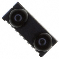
Vishay Semiconductors
PINOUT
TFDU4101
Weight 200 mg
”U” Option Baby Face (universal)
IRED
1
2
Detector
3
4
5
6
7 8
17087
ABSOLUTE MAXIMUM RATINGS
PARAMETER
TEST CONDITIONS
SYMBOL
MIN.
TYP.
MAX.
UNIT
-0.3 V < VCC2 < 6 V
VCC1
-0.5
-
6
V
Supply voltage range, transmitter
-0.5 V < VCC1 < 6 V
VCC2
-0.5
-
6
V
Voltage at RXD
-0.5 V < VCC1 < 6 V
VRXD
-0.5
-
VCC1 + 0.5
V
Vin > VCC1 is allowed
Vin
-0.5
-
6
V
Supply voltage range, transceiver
Voltage at all inputs and outputs
Input currents
For all pins, except IRED anode pin
Output sinking current
-
-
10
mA
-
-
25
mA
Power dissipation
PD
-
-
250
mW
Junction temperature
TJ
-
-
125
°C
Tamb
-30
-
+85
°C
Tstg
-30
-
+85
°C
-
-
260
°C
IIRED (DC)
-
-
80
mA
Ambient temperature range (operating)
Storage temperature range
Soldering temperature
See “Recommended Solder Profile”
Average output current, pin 1
Repetitive pulse output current, pin 1 to
pin 2
< 90 μs, ton < 20 %
IIRED (RP)
-
-
400
mA
Thermal resistance junction-to-ambient
JESD51
RthJA
-
300
-
K/W
Note
• Reference point pin, GND unless otherwise noted. Typical values are for DESIGN AID ONLY, not guaranteed nor subject to production
testing
EYE SAFETY INFORMATION
STANDARD
CLASSIFICATION
IEC/EN 60825-1 (2007-03), DIN EN 60825-1 (2008-05) “SAFETY OF LASER PRODUCTS Part 1: equipment classification and requirements”, simplified method
Class 1
IEC 62471 (2006), CIE S009 (2002) “Photobiological Safety of Lamps and Lamp Systems”
Exempt
DIRECTIVE 2006/25/EC OF THE EUROPEAN PARLIAMENT AND OF THE COUNCIL of 5th April 2006
on the minimum health and safety requirements regarding the exposure of workers to risks arising
from physical agents (artificial optical radiation) (19th individual directive within the meaning of article
16(1) of directive 89/391/EEC)
Exempt
Note
• Vishay transceivers operating inside the absolute maximum ratings are classified as eye safe according the above table
Rev. 2.2, 25-Jul-2022
Document Number: 81288
3
For technical questions within your region: irdasupportAM@vishay.com, irdasupportAP@vishay.com, irdasupportEU@vishay.com
THIS DOCUMENT IS SUBJECT TO CHANGE WITHOUT NOTICE. THE PRODUCTS DESCRIBED HEREIN AND THIS DOCUMENT
ARE SUBJECT TO SPECIFIC DISCLAIMERS, SET FORTH AT www.vishay.com/doc?91000
�TFDU4101
www.vishay.com
Vishay Semiconductors
ELECTRICAL CHARACTERISTICS (Tamb = 25 °C, VCC1 = VCC2 = 2.4 V to 5.5 V unless otherwise noted)
PARAMETER
TEST CONDITIONS/PINS
SYMBOL
MIN.
TYP.
MAX.
UNIT
TRANSCEIVER
Supply voltage
VCC1
2.4
-
5.5
V
Dynamic supply current
SD = low, Ee = 1 klx (1),
Tamb = -25 °C to +85 °C
VCC1 = VCC2 = 2.4 V to 5.5 V
ICC1
40
90
130
μA
Dynamic supply current
SD = low, Ee = 1 klx (1),
Tamb = 25 °C
VCC1 = VCC2 = 2.4 V to 5.5 V
ICC1
40
75
-
μA
Average dynamic supply
current, transmitting
IIRED = 300 mA,
25 % duty cycle
ICC
-
0.65
2.5
mA
SD = high, T = 25 °C, Ee = 0 klx
no signal, no resistive load
ISD
-
0.01
0.1
μA
SD = high, T = 70 °C
no signal, no resistive load
ISD
-
-
1
μA
SD = high, T = 85 °C
no signal, no resistive load
ISD
-
-
1
μA
TA
-30
-
+85
°C
Shutdown supply current
Operating temperature range
Output voltage low, RXD
Output voltage high, RXD
Cload = 15 pF
VOL
-0.5
-
0.15 x VCC1
V
IOH = -500 μA, CLoad = 15 pF
VOH
0.8 x VCC1
-
VCC1 + 0.5
V
IOH = -250 μA, CLoad = 15 pF
VOH
0.9 x VCC1
-
VCC1 + 0.5
V
RRXD
400
500
600
kΩ
V
RXD to VCC1 impedance
Input voltage low (TXD, SD)
SD = high
VIL
-0.5
-
0.5
VIH
VCC1 - 0.5
-
6
V
Vin = 0.9 x VCC1
IICH
-2
-
+2
μA
SD, TXD = “0” or “1”
IIrTX
-1
0
+150
1
μA
μA
-
-
5
pF
Input voltage high (TXD, SD)
Input leakage current (TXD, SD)
Controlled pull down current
0 < Vin < 0.15 VCC1
Vin > 0.7 VCC1
Input capacitance (TXD, SD)
CI
Notes
• Typical values are for DESIGN AID ONLY, not guaranteed nor subject to production testing
(1) Standard illuminant A
(2) The typical threshold level is 0.5 x V
CC1. It is recommended to use the specified min./max. values to avoid increased operating current
Rev. 2.2, 25-Jul-2022
Document Number: 81288
4
For technical questions within your region: irdasupportAM@vishay.com, irdasupportAP@vishay.com, irdasupportEU@vishay.com
THIS DOCUMENT IS SUBJECT TO CHANGE WITHOUT NOTICE. THE PRODUCTS DESCRIBED HEREIN AND THIS DOCUMENT
ARE SUBJECT TO SPECIFIC DISCLAIMERS, SET FORTH AT www.vishay.com/doc?91000
�TFDU4101
www.vishay.com
Vishay Semiconductors
OPTOELECTRONIC CHARACTERISTICS (Tamb = 25 °C, VCC1 = VCC2 = 2.4 V to 5.5 V unless otherwise noted)
PARAMETER
TEST CONDITIONS
SYMBOL
MIN.
TYP.
MAX.
UNIT
Minimum irradiance Ee in
angular range (2) SIR mode
9.6 kbit/s to 115.2 kbit/s
λ = 850 nm to 900 nm; α = 0°, 15°
Ee, min.
4
(0.4)
20
(2)
35 (1)
(3.5)
mW/m2
(μW/cm2)
Maximum irradiance Ee in
angular range (3)
λ = 850 nm to 900 nm
Ee, max.
5
(500)
-
-
kW/m2
(mW/cm2)
Rise time of output signal
10 % to 90 %, CL = 15 pF
tr (RXD)
20
-
100
ns
Fall time of output signal
90 % to 10 %, CL = 15 pF
tf (RXD)
20
-
100
ns
RXD pulse width
Input pulse length > 1.2 μs
tPW
1.65
2.2
3
μs
Input irradiance = 100 mW/m2,
≤ 115.2 kbit/s
-
-
250
ns
After shutdown active or power-on
-
100
500
μs
-
100
150
μs
RECEIVER
Leading edge jitter
Standby/shutdown delay,
receiver startup time
Latency
tL
TRANSMITTER (new surface emitter values introduced via PCN OPT-1210-2022)
IRED operating current
limitation
Forward voltage of built-in
IRED
Output leakage IRED current
Output radiant intensity
No external resistor for current limitation (4)
ID
200
300
430
mA
If = 300 mA
Vf
1.4
1.8
1.9
V
TXD = 0 V, 0 < VCC1 < 5.5 V
IIRED
-1
0.01
1
μA
α = 0°, 15°, TXD = high, SD = low
Ie
50
150
400
mW/sr
VCC1 = 5 V, α = 0°, 15°,
TXD = low or SD = high
(receiver is inactive as long as SD = high)
Ie
-
-
0.04
mW/sr
α
-
± 30
-
°
λp
870
-
910
nm
Δλ
-
45
-
nm
50
Output radiant intensity, angle
of half intensity
Peak - emission
wavelength (5)
Spectral bandwidth
Optical rise time, fall time
Optical output pulse duration
tropt, tfopt
10
Input pulse width 1.6 < tTXD < 23 μs
topt
tTXD - 0.15
Input pulse width tTXD ≥ 23 μs
topt
23
Optical overshoot
50
100
ns
tTXD + 0.15
μs
100
μs
25
%
Notes
• Typical values are for DESIGN AID ONLY, not guaranteed nor subject to production testing
(1) IrDA specification is 40 mW/m2. Specification takes a window loss of 10 % into account
(2) IrDA sensitivity definition: minimum irradiance E in angular range, power per unit area. The receiver must meet the BER specification while
e
the source is operating at the minimum intensity in angular range into the minimum half-angular range at the maximum link length
(3) Maximum irradiance E in angular range, power per unit area. The optical delivered to the detector by a source operating at the maximum
e
intensity in angular range at minimum link length must not cause receiver overdrive distortion and possible ralated link errors. If placed at
the active output interface reference plane of the transmitter, the receiver must meet its bit error ratio (BER) specification
(4) Using an external current limiting resistor is allowed and recommended to reduce IRED intensity and operating current when current
reduction is intended to operate at the IrDA low power conditions. E.g. for VCC2 = 3.3 V a current limiting resistor of RS = 56 Ω will allow a
power minimized operation at IrDA low power conditions
(5) Due to this wavelength restriction compared to the IrDA spec of 850 nm to 900 nm the transmitter is able to operate as source for the
standard remote control applications with codes as e.g. Phillips RC5/RC6® or RECS 80
For more definitions see the document “Symbols and Terminology” on the Vishay website.
Rev. 2.2, 25-Jul-2022
Document Number: 81288
5
For technical questions within your region: irdasupportAM@vishay.com, irdasupportAP@vishay.com, irdasupportEU@vishay.com
THIS DOCUMENT IS SUBJECT TO CHANGE WITHOUT NOTICE. THE PRODUCTS DESCRIBED HEREIN AND THIS DOCUMENT
ARE SUBJECT TO SPECIFIC DISCLAIMERS, SET FORTH AT www.vishay.com/doc?91000
�TFDU4101
www.vishay.com
Vishay Semiconductors
RECOMMENDED CIRCUIT DIAGRAM
Operated with a clean low impedance power supply the
TFDU4101 needs no additional external components.
However, depending on the entire system design and board
layout, additional components may be required (see figure
1). That is especially the case when separate power supplies
are used for bench tests. When using compact wiring and
regulated supplies as e. g. in phone applications in most
cases no external components are necessary.
VIRED
R1(1)
VCC
R2
GND
C1
VCC2, IRED A
VCC1
C2
Ground
SD
SD
TXD
TXD
RXD
RXD
20037
IRED C
Fig. 1 - Recommended Test Circuit
Note
(1) R1 is optional when reduced intensity is used
The capacitor C1 is buffering the supply voltage and
eliminates the inductance of the power supply line. This one
should be a Tantalum or other fast capacitor to guarantee
the fast rise time of the IRED current. The resistor R1 is the
current limiting resistor, which may be used to reduce the
operating current to levels below the specified controlled
values for saving battery power.
Vishay's transceivers integrate a sensitive receiver and a
built-in power driver. The combination of both needs a
careful circuit board layout. The use of thin, long, resistive
and inductive wiring should be avoided. The shutdown input
must be grounded for normal operation, also when the
shutdown function is not used.
The inputs (TXD, SD) and the output RXD should be directly
connected (DC-coupled) to the I/O circuit. The capacitor C2
combined with the resistor R2 is the low pass filter for
smoothing the supply voltage. R2, C1 and C2 are optional
and dependent on the quality of the supply voltages VCC1
and injected noise. An unstable power supply with dropping
voltage during transmission may reduce the sensitivity (and
transmission range) of the transceiver.
The placement of these parts is critical. It is strongly
recommended to position C2 as close as possible to the
transceiver power supply pins.
When extended wiring is used (bench tests!) the inductance
of the power supply can cause dynamically a voltage drop
at VCC2. Often some power supplies are not able to follow
the fast current rise time. In that case another 4.7 μF (type,
see table under C1) at VCC2 will be helpful.
Under extreme EMI conditions as placing an
RF-transmitter antenna on top of the transceiver, we
recommend to protect all inputs by a low-pass filter, as a
minimum a 12 pF capacitor, especially at the RXD port. The
transceiver itself withstands EMI at GSM frequencies above
500 V/m. When interference is observed, the wiring to the
inputs picks it up. It is verified by DPI measurements that as
long as the interfering RF - voltage is below the logic
threshold levels of the inputs and equivalent levels at the
outputs no interferences are expected.
One should keep in mind that basic RF-design rules for
circuit design should be taken into account. Especially
longer signal lines should not be used without termination.
See e.g. “The Art of Electronics” Paul Horowitz, Winfield Hill,
1989, Cambridge University Press, ISBN: 0521370957.
TABLE 1 - RECOMMENDED TESTS AND APPLICATION CIRCUIT COMPONENTS
COMPONENT
RECOMMENDED VALUE
VISHAY PART NUMBER
C1
4.7 μF, 16 V
293D 475X9 016B
0.1 μF, ceramic
VJ 1206 Y 104 J XXMT
C2
R1
R2
Depends on current to be adjusted, e. g. with VCC2 = 3.3 V 56 Ω is an option for minimum low power operation
47 Ω, 0.125 W
Figure 2 shows an example of a typical application with a
separate supply voltage VS and using the transceiver with
the IRED anode connected to the unregulated battery Vbatt.
This method reduces the peak load of the regulated power
supply and saves therefore costs. Alternatively all supplies
can also be tied to only one voltage source. R1 and C1 are
not used in this case and are depending on the circuit
design in most cases not necessary.
CRCW-1206-47R0-F-RT1
In Fig. 2 an option is shown to operate the transmitter at two
different power levels to switch for long range to low power
mode for e.g. saving power for IrDA application but use the
full range specification for remote control. The additional
components are marked in the figure.
For operating at RS232 ports we recommend to use an
encoder / decoder-module.
Rev. 2.2, 25-Jul-2022
Document Number: 81288
6
For technical questions within your region: irdasupportAM@vishay.com, irdasupportAP@vishay.com, irdasupportEU@vishay.com
THIS DOCUMENT IS SUBJECT TO CHANGE WITHOUT NOTICE. THE PRODUCTS DESCRIBED HEREIN AND THIS DOCUMENT
ARE SUBJECT TO SPECIFIC DISCLAIMERS, SET FORTH AT www.vishay.com/doc?91000
�TFDU4101
www.vishay.com
Vishay Semiconductors
I/O AND SOFTWARE
Vbatt 3 V
Hi/Low
Vs = 2.8 V
C1
R1
Vdd
IRTX
IRRX
IR MODE
R2
IRED anode (1)
IRED cathode (2)
TXD (3)
RXD (4)
SD (5)
VCC1 (6)
In the description, already different I/Os are mentioned.
Different combinations are tested and the function verified
with the special drivers available from the I/O suppliers. In
special cases refer to the I/O manual, the Vishay application
notes, or contact directly Vishay Sales, Marketing or
Application.
C2
GND (8)
20038
Fig. 2 - Typical Application Circuit
Grey: Optional for High/Low Switching
TABLE 2 - TRUTH TABLE
INPUTS
OUTPUTS
REMARK
SD
TXD
OPTICAL INPUT IRRADIANCE
mW/m2
High
> 1 ms
x
x
High < 50 μs
x
Low active
Ie
Transmitting
High > 50 μs
x
High inactive
0
Protection is active
Low
min. irradiance Ee
< max. irradiance Ee
Low (active)
0
Response to an IrDA compliant
optical input signal
Low
> max. irradiance Ee
Undefined
0
Overload conditions can cause
unexpected outputs
RXD
TRANSMITTER
OPERATION
Weakly pulled
(500 kΩ) to VCC1
0
Shutdown
Low
Rev. 2.2, 25-Jul-2022
Document Number: 81288
7
For technical questions within your region: irdasupportAM@vishay.com, irdasupportAP@vishay.com, irdasupportEU@vishay.com
THIS DOCUMENT IS SUBJECT TO CHANGE WITHOUT NOTICE. THE PRODUCTS DESCRIBED HEREIN AND THIS DOCUMENT
ARE SUBJECT TO SPECIFIC DISCLAIMERS, SET FORTH AT www.vishay.com/doc?91000
�TFDU4101
www.vishay.com
Vishay Semiconductors
ASSEMBLY INSTRUCTIONS
Reflow Soldering
• Reflow soldering must be done within 72 h while stored
under a max. temperature of 30 °C, 60 % RH after
opening the dry pack envelope
• Set the furnace temperatures for pre-heating and heating
in accordance with the reflow temperature profile as
shown in the diagram. Exercise extreme care to keep the
maximum temperature below 260 °C. The temperature
shown in the profile means the temperature at the device
surface. Since there is a temperature difference between
the component and the circuit board, it should be verified
that the temperature of the device is accurately being
measured
• Handling after reflow should be done only after the work
surface has been cooled off
Manual Soldering
• Use a soldering iron of 25 W or less. Adjust the
temperature of the soldering iron below 300 °C
• Finish soldering within 3 s
• Handle products only after the temperature has cooled off
VISHAY LEAD (Pb)-FREE REFLOW SOLDER PROFILE
Axis Title
10000
300
255 °C
240 °C
250
245 °C
217 °C
200
1000
max. 20 s
150
max. 120 s
max. 100 s
100
100
Max. ramp up 3 °C/s
50
Max. ramp down 6 °C/s
Max. 2 cycles allowed
0
0
19800
1st line
2nd line
2nd line
Temperature (°C)
max. 260 °C
50
100
150
200
250
10
300
Time (s)
Rev. 2.2, 25-Jul-2022
Document Number: 81288
8
For technical questions within your region: irdasupportAM@vishay.com, irdasupportAP@vishay.com, irdasupportEU@vishay.com
THIS DOCUMENT IS SUBJECT TO CHANGE WITHOUT NOTICE. THE PRODUCTS DESCRIBED HEREIN AND THIS DOCUMENT
ARE SUBJECT TO SPECIFIC DISCLAIMERS, SET FORTH AT www.vishay.com/doc?91000
�TFDU4101
www.vishay.com
Vishay Semiconductors
PACKAGE DIMENSIONS in millimeters
7x1=7
0.6
2.5
1
8
18470
1
Fig. 3 - Package Drawing TFDU4101. Tolerance ± 0.2 mm if not otherwise mentioned
20035
Fig. 4 - Recommended Footprint for Side View Applications and Solderpaste Mask
Rev. 2.2, 25-Jul-2022
Document Number: 81288
9
For technical questions within your region: irdasupportAM@vishay.com, irdasupportAP@vishay.com, irdasupportEU@vishay.com
THIS DOCUMENT IS SUBJECT TO CHANGE WITHOUT NOTICE. THE PRODUCTS DESCRIBED HEREIN AND THIS DOCUMENT
ARE SUBJECT TO SPECIFIC DISCLAIMERS, SET FORTH AT www.vishay.com/doc?91000
�TFDU4101
www.vishay.com
Vishay Semiconductors
20036
Fig. 5 - Recommended Footprint for Top View Applications and Solderpaste Mask
TAPE DIMENSIONS FOR TT3 in millimeters
Drawing-No.: 9.700-5251.01-4
Issue: 3; 02.09.05
19824
Fig. 6 - Tape Drawing, TFDU4101 for Top View Mounting, Tolerance ± 0.1 mm
Rev. 2.2, 25-Jul-2022
Document Number: 81288
10
For technical questions within your region: irdasupportAM@vishay.com, irdasupportAP@vishay.com, irdasupportEU@vishay.com
THIS DOCUMENT IS SUBJECT TO CHANGE WITHOUT NOTICE. THE PRODUCTS DESCRIBED HEREIN AND THIS DOCUMENT
ARE SUBJECT TO SPECIFIC DISCLAIMERS, SET FORTH AT www.vishay.com/doc?91000
�TFDU4101
www.vishay.com
Vishay Semiconductors
TAPE DIMENSIONS FOR TR3 in millimeters
19875
Fig. 7 - Tape Drawing, TFDU4101 for Side View Mounting, Tolerance ± 0.1 mm
Rev. 2.2, 25-Jul-2022
Document Number: 81288
11
For technical questions within your region: irdasupportAM@vishay.com, irdasupportAP@vishay.com, irdasupportEU@vishay.com
THIS DOCUMENT IS SUBJECT TO CHANGE WITHOUT NOTICE. THE PRODUCTS DESCRIBED HEREIN AND THIS DOCUMENT
ARE SUBJECT TO SPECIFIC DISCLAIMERS, SET FORTH AT www.vishay.com/doc?91000
�TFDU4101
www.vishay.com
Vishay Semiconductors
REEL DIMENSIONS in millimeters
Drawing-No.: 9.800-5090.01-4
Issue: 1; 29.11.05
14017
TAPE WIDTH
(mm)
A MAX.
(mm)
N
(mm)
W1 MIN.
(mm)
W2 MAX.
(mm)
W3 MIN.
(mm)
W3 MAX.
(mm)
24
330
60
24.4
30.4
23.9
27.4
LEADER AND TRAILER DIMENSIONS in millimeters
Trailer
no devices
Leader
devices
no devices
End
Start
min. 200
min. 400
96 11818
COVER TAPE PEEL STRENGTH
LABEL
According to DIN EN 60286-3
0.1 N to 1.3 N
300 ± 10 mm/min.
165° to 180° peel angle
Standard bar code labels for finished goods
The standard bar code labels are product labels and used
for identification of goods. The finished goods are packed in
final packing area. The standard packing units are labeled
with standard bar code labels before transported as finished
goods to warehouses. The labels are on each packing unit
and contain Vishay Semiconductor GmbH specific data.
Rev. 2.2, 25-Jul-2022
Document Number: 81288
12
For technical questions within your region: irdasupportAM@vishay.com, irdasupportAP@vishay.com, irdasupportEU@vishay.com
THIS DOCUMENT IS SUBJECT TO CHANGE WITHOUT NOTICE. THE PRODUCTS DESCRIBED HEREIN AND THIS DOCUMENT
ARE SUBJECT TO SPECIFIC DISCLAIMERS, SET FORTH AT www.vishay.com/doc?91000
�TFDU4101
www.vishay.com
Vishay Semiconductors
DRY PACKING
The reel is packed in an anti-humidity bag to protect the
devices from absorbing moisture during transportation and
storage.
Aluminum bag
Label
After more than 72 h under these conditions moisture
content will be too high for reflow soldering.
In case of moisture absorption, the devices will recover to
the former condition by drying under the following condition:
192 h at 40 °C + 5 °C / - 0 °C and < 5 % RH (dry air /
nitrogen) or
96 h at 60 °C + 5 °C and < 5 % RH for all device containers
or
24 h at 125 °C + 5 °C not suitable for reel or tubes.
An EIA JEDEC® standard J-STD-020 level 4 label is included
on all dry bags.
Reel
CAUTION
15973
This bag contains
MOISTURE-SENSITIVE DEVICES
FINAL PACKING
LEVEL
4
1. Shelf life in sealed bag: 12 months at < 40 °C and < 90 % relative
humidity (RH)
The sealed reel is packed into a cardboard box.
2. After this bag is opened, devices that will be subjected to soldering
reflow or equivalent processing (peak package body temp. 260 °C)
must be
2a. Mounted within 72 hours at factory condition of < 30 °C/60 % RH or
2b. Stored at < 5 % RH
RECOMMENDED METHOD OF STORAGE
3. Devices require baking befor mounting if:
Humidity Indicator Card is > 10 % when read at 23 °C ± 5 °C or
2a. or 2b. are not met.
Dry box storage is recommended as soon as the aluminum
bag has been opened to prevent moisture absorption. The
following conditions should be observed, if dry boxes are
not available:
• Storage temperature 10 °C to 30 °C
• Storage humidity ≤ 60 % RH max.
4. If baking is required, devices may be baked for:
192 hours at 40 °C + 5 °C/- 0 °C and < 5 % RH (dry air/nitrogen) or
96 hours at 60 °C ± 5 °C and < 5 % RH for all device containers or
24 hours at 125 °C ± 5 °C not suitable for reels or tubes
Bag Seal Date:
(If blank, see barcode label)
Note: Level and body temperature defined by EIA JEDEC Standard J-STD-020
22522
EIA JEDEC standard J-STD-020 level 4 label is included
on all dry bags
OUTER PACKAGING
The sealed reel is packed into a pizza box.
CARTON BOX DIMENSIONS in millimeters
Length
Thickness
22127
ORDER CODE
Width
BOXING
THICKNESS
WIDTH
LENGTH
TT3 / TR3
Pizza box (taping in reels)
50
340
340
TT1 / TR1
Pizza box (taping in reels)
32
190
190
Rev. 2.2, 25-Jul-2022
Document Number: 81288
13
For technical questions within your region: irdasupportAM@vishay.com, irdasupportAP@vishay.com, irdasupportEU@vishay.com
THIS DOCUMENT IS SUBJECT TO CHANGE WITHOUT NOTICE. THE PRODUCTS DESCRIBED HEREIN AND THIS DOCUMENT
ARE SUBJECT TO SPECIFIC DISCLAIMERS, SET FORTH AT www.vishay.com/doc?91000
�TFDU4101
www.vishay.com
Vishay Semiconductors
VISHAY SEMICONDUCTOR GmbH STANDARD BAR CODE PRODUCT LABEL (finished goods)
PLAIN WRITING
ABBREVIATION
LENGTH
Item-description
-
18
Item-number
INO
8
Selection-code
SEL
3
BATCH
10
Data-code
COD
3 (YWW)
Plant-code
PTC
2
Quantity
QTY
8
Accepted by
ACC
-
Packed by
PCK
-
LOT-/serial-number
Mixed code indicator
MIXED CODE
-
xxxxxxx+
Company logo
Origin
Long bar code top
Type
Length
Item-number
N
8
Plant-code
N
2
Sequence-number
X
3
Quantity
N
8
Total length
-
21
Short bar code bottom
Type
Length
Selection-code
X
3
Data-code
N
3
Batch-number
X
10
Filter
-
1
Total length
-
17
The Vishay Semiconductors standard bar code labels are printed at final packing areas. The labels are on each packing unit and
contain Vishay Semiconductors specific data.
Lead (Pb)-free category
e3 Sn
Lot 1: lot number or identification
Lot 2: 1920031A91
19 – plant code
20 – year
03 – workweek
1 – weekday: 1 Mon, 2 Tue, …
A – shift
91 – printer number
QA acceptance seal
Device type
Quantity
Plant location
Plant location code
23195
Batch number
YYYYWW
+ country
+ plant code
RoHS compliance
logo
Lead (Pb)-free
logo
Fig. 8 - 2D Bar Code Label (according the bar code standard for 2D label PDF 417)
for a Lead (Pb)-Free Device Made in Philippines, Detailed Description
ESD PRECAUTION
Proper storage and handling procedures should be followed to prevent ESD damage to the devices especially when they are
removed from the antistatic shielding bag. Electrostatic sensitive devices warning labels are on the packaging.
Rev. 2.2, 25-Jul-2022
Document Number: 81288
14
For technical questions within your region: irdasupportAM@vishay.com, irdasupportAP@vishay.com, irdasupportEU@vishay.com
THIS DOCUMENT IS SUBJECT TO CHANGE WITHOUT NOTICE. THE PRODUCTS DESCRIBED HEREIN AND THIS DOCUMENT
ARE SUBJECT TO SPECIFIC DISCLAIMERS, SET FORTH AT www.vishay.com/doc?91000
�Legal Disclaimer Notice
www.vishay.com
Vishay
Disclaimer
ALL PRODUCT, PRODUCT SPECIFICATIONS AND DATA ARE SUBJECT TO CHANGE WITHOUT NOTICE TO IMPROVE
RELIABILITY, FUNCTION OR DESIGN OR OTHERWISE.
Vishay Intertechnology, Inc., its affiliates, agents, and employees, and all persons acting on its or their behalf (collectively,
“Vishay”), disclaim any and all liability for any errors, inaccuracies or incompleteness contained in any datasheet or in any other
disclosure relating to any product.
Vishay makes no warranty, representation or guarantee regarding the suitability of the products for any particular purpose or
the continuing production of any product. To the maximum extent permitted by applicable law, Vishay disclaims (i) any and all
liability arising out of the application or use of any product, (ii) any and all liability, including without limitation special,
consequential or incidental damages, and (iii) any and all implied warranties, including warranties of fitness for particular
purpose, non-infringement and merchantability.
Statements regarding the suitability of products for certain types of applications are based on Vishay's knowledge of typical
requirements that are often placed on Vishay products in generic applications. Such statements are not binding statements
about the suitability of products for a particular application. It is the customer's responsibility to validate that a particular product
with the properties described in the product specification is suitable for use in a particular application. Parameters provided in
datasheets and / or specifications may vary in different applications and performance may vary over time. All operating
parameters, including typical parameters, must be validated for each customer application by the customer's technical experts.
Product specifications do not expand or otherwise modify Vishay's terms and conditions of purchase, including but not limited
to the warranty expressed therein.
Hyperlinks included in this datasheet may direct users to third-party websites. These links are provided as a convenience and
for informational purposes only. Inclusion of these hyperlinks does not constitute an endorsement or an approval by Vishay of
any of the products, services or opinions of the corporation, organization or individual associated with the third-party website.
Vishay disclaims any and all liability and bears no responsibility for the accuracy, legality or content of the third-party website
or for that of subsequent links.
Except as expressly indicated in writing, Vishay products are not designed for use in medical, life-saving, or life-sustaining
applications or for any other application in which the failure of the Vishay product could result in personal injury or death.
Customers using or selling Vishay products not expressly indicated for use in such applications do so at their own risk. Please
contact authorized Vishay personnel to obtain written terms and conditions regarding products designed for such applications.
No license, express or implied, by estoppel or otherwise, to any intellectual property rights is granted by this document or by
any conduct of Vishay. Product names and markings noted herein may be trademarks of their respective owners.
© 2022 VISHAY INTERTECHNOLOGY, INC. ALL RIGHTS RESERVED
Revision: 01-Jan-2022
1
Document Number: 91000
�


 工商网监
湘ICP备2023018690号
工商网监
湘ICP备2023018690号
