V12P12
www.vishay.com
Vishay General Semiconductor
High Current Density Surface-Mount
Trench MOS Barrier Schottky Rectifier
Ultra Low VF = 0.51 V at IF = 6 A
FEATURES
eSMP® Series
• Very low profile - typical height of 1.1 mm
Available
• Ideal for automated placement
• Trench MOS Schottky technology
K
• Low forward voltage drop, low power losses
• High efficiency operation
1
• Meets MSL level 1, per
LF maximum peak of 260 °C
2
J-STD-020,
• AEC-Q101 qualified available
- Automotive ordering code; base P/NHM3
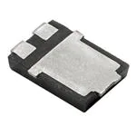
SMPC (TO-277A)
K
Anode 1
Cathode
Anode 2
• Material categorization: for definitions of compliance
please see www.vishay.com/doc?99912
TYPICAL APPLICATIONS
ADDITIONAL RESOURCES
For use in low voltage high frequency inverters,
freewheeling, DC/DC converters and polarity protection
applications.
3D 3D
3D Models
MECHANICAL DATA
PRIMARY CHARACTERISTICS
IF(AV)
12 A
VRRM
120 V
IFSM
150 A
EAS
100 mJ
VF at IF = 12 A
0.63 V
TJ max.
150 °C
Package
SMPC (TO-277A)
Circuit configuration
Single
Case: SMPC (TO-277A)
Molding compound meets UL 94 V-0 flammability rating
Base P/N-M3 - halogen-free, RoHS-compliant, and
commercial grade
Base P/NHM3_X - halogen-free, RoHS-compliant and
AEC-Q101 qualified
(“_X” denotes revision code e.g. A, B,.....)
Terminals: matte tin plated leads, solderable per
J-STD-002 and JESD 22-B102
M3 suffix meets JESD 201 class 1A whisker test, HM3 suffix
meets JESD 201 class 2 whisker test
MAXIMUM RATINGS (TA = 25 °C unless otherwise noted)
PARAMETER
SYMBOL
Device marking code
V12P12
UNIT
V1212
Maximum repetitive peak reverse voltage
VRRM
120
V
Maximum average forward rectified current (fig. 1)
IF(AV)
12
A
Peak forward surge current 10 ms single half sine-wave
superimposed on rated load
IFSM
150
A
Non-repetitive avalanche energy at IAS = 2.0 A, L = 50 mH, TJ = 25 °C
EAS
100
mJ
Peak repetitive reverse current at tp = 2 μs, 1 kHz, TJ = 38 °C ± 2 °C
Operating junction and storage temperature range
IRRM
0.5
A
TJ, TSTG
-40 to +150
°C
Revision: 11-Dec-2019
Document Number: 89094
1
For technical questions within your region: DiodesAmericas@vishay.com, DiodesAsia@vishay.com, DiodesEurope@vishay.com
THIS DOCUMENT IS SUBJECT TO CHANGE WITHOUT NOTICE. THE PRODUCTS DESCRIBED HEREIN AND THIS DOCUMENT
ARE SUBJECT TO SPECIFIC DISCLAIMERS, SET FORTH AT www.vishay.com/doc?91000
�V12P12
www.vishay.com
Vishay General Semiconductor
ELECTRICAL CHARACTERISTICS (TA = 25 °C unless otherwise noted)
PARAMETER
TEST CONDITIONS
Breakdown voltage
IR = 1.0 mA
IF = 6 A
SYMBOL
TYP.
MAX.
UNIT
VBR
120 (minimum)
-
V
0.57
-
0.72
0.80
0.51
-
0.63
0.70
TA = 25 °C
13
-
μA
TA = 125 °C
7
-
mA
50
500
μA
16
50
mA
TA = 25 °C
IF = 12 A
Instantaneous forward voltage
TA = 25 °C
VF (1)
IF = 6 A
TA = 125 °C
IF = 12 A
VR = 90 V
Reverse current
VR = 120 V
TA = 25 °C
IR (2)
TA = 125 °C
V
Notes
(1) Pulse test: 300 μs pulse width, 1 % duty cycle
(2) Pulse test: Pulse width ≤ 40 ms
THERMAL CHARACTERISTICS (TA = 25 °C unless otherwise noted)
PARAMETER
SYMBOL
RθJA
Typical thermal resistance
V12P12
(1)
60
RθJL
4
UNIT
°C/W
Note
(1) Units mounted on recommended PCB 1 oz. pad layout
ORDERING INFORMATION (Example)
PREFERRED P/N
UNIT WEIGHT (g)
PREFERRED PACKAGE CODE
BASE QUANTITY
DELIVERY MODE
V12P12-M3/86A
0.10
86A
1500
7" diameter plastic tape and reel
V12P12-M3/87A
0.10
87A
6500
13" diameter plastic tape and reel
V12P12HM3_A/H (1)
0.10
H
1500
7" diameter plastic tape and reel
V12P12HM3_A/I (1)
0.10
I
6500
13" diameter plastic tape and reel
Note
AEC-Q101 qualified
(1)
Revision: 11-Dec-2019
Document Number: 89094
2
For technical questions within your region: DiodesAmericas@vishay.com, DiodesAsia@vishay.com, DiodesEurope@vishay.com
THIS DOCUMENT IS SUBJECT TO CHANGE WITHOUT NOTICE. THE PRODUCTS DESCRIBED HEREIN AND THIS DOCUMENT
ARE SUBJECT TO SPECIFIC DISCLAIMERS, SET FORTH AT www.vishay.com/doc?91000
�V12P12
www.vishay.com
Vishay General Semiconductor
RATINGS AND CHARACTERISTICS CURVES (TA = 25 °C unless otherwise noted)
Axis Title
10000
100
Resistive or Inductive Load
12
10
8
6
TL Measured
at the Cathode Band Terminal
4
2
0
100
110
120
130
140
10
TJ = 150 °C
TJ = 125 °C
1
0.1
100
0.01
TJ = 25 °C
0.001
TJ = -40 °C
10
0.0001
150
20
40
Lead Temperature (°C)
60
80
100
Percent of Rated Peak Reverse Voltage (%)
Fig. 1 - Maximum Forward Current Derating Curve
Fig. 4 - Typical Reverse Characteristics
10 000
11
D = 0.3
10
D = 0.2
9
8
D = 0.1
7
TJ = 25 °C
f = 1.0 MHz
Vsig = 50 mVp-p
D = 0.5 D = 0.8
Junction Capacitance (pF)
Average Power Loss (W)
1000
TJ = 100 °C
1 t li
2nd line
Instantaneous Reverse Current (mA)
Average Forward Rectified Current (A)
14
D = 1.0
6
5
T
4
3
2
D = tp/T
1
1000
100
tp
10
0
0
2
4
6
8
10
12
0.1
14
1
10
100
Reverse Voltage (V)
Average Forward Current (A)
Fig. 2 - Forward Power Loss Characteristics
Fig. 5 - Typical Junction Capacitance
Axis Title
100
10000
T J = 150 °C
10
1000
T J = 125 ° C
1
T J = 100 °C
100
T J = 25 °C
0.1
T J = -40 °C
0.01
10
0
0.1 0.2 0.3 0.4 0.5 0.6 0.7 0.8 0.9 1.0
Instantaneous Forward Voltage (V)
Fig. 3 - Typical Instantaneous Forward Characteristics
Transient Thermal Impedance (°C/W)
2nd line
Instantaneous Forward Current (A)
100
Junction to Ambient
10
1
0.01
0.1
1
10
100
t - Pulse Duration (s)
Fig. 6 - Typical Transient Thermal Impedance
Revision: 11-Dec-2019
Document Number: 89094
3
For technical questions within your region: DiodesAmericas@vishay.com, DiodesAsia@vishay.com, DiodesEurope@vishay.com
THIS DOCUMENT IS SUBJECT TO CHANGE WITHOUT NOTICE. THE PRODUCTS DESCRIBED HEREIN AND THIS DOCUMENT
ARE SUBJECT TO SPECIFIC DISCLAIMERS, SET FORTH AT www.vishay.com/doc?91000
�V12P12
www.vishay.com
Vishay General Semiconductor
PACKAGE OUTLINE DIMENSIONS in inches (millimeters)
SMPC (TO-277A)
0.187 (4.75)
0.175 (4.45)
0.016 (0.40)
0.006 (0.15)
K
0.262 (6.65)
0.250 (6.35)
0.242 (6.15)
0.238 (6.05)
2
1
0.047 (1.20)
0.039 (1.00)
0.171 (4.35)
0.167 (4.25)
0.146 (3.70)
0.134 (3.40)
Mounting Pad Layout
0.087 (2.20)
0.075 (1.90)
0.189 (4.80)
MIN.
0.189 (4.80)
0.173 (4.40)
0.186 (4.72)
MIN.
0.268
(6.80)
0.155 (3.94)
NOM.
0.030 (0.75) NOM.
0.049 (1.24)
0.037 (0.94)
0.050 (1.27)
MIN.
0.084 (2.13) NOM.
0.053 (1.35)
0.041 (1.05)
0.041
(1.04)
0.055 (1.40)
MIN.
Conform to JEDEC® TO-277A
Revision: 11-Dec-2019
Document Number: 89094
4
For technical questions within your region: DiodesAmericas@vishay.com, DiodesAsia@vishay.com, DiodesEurope@vishay.com
THIS DOCUMENT IS SUBJECT TO CHANGE WITHOUT NOTICE. THE PRODUCTS DESCRIBED HEREIN AND THIS DOCUMENT
ARE SUBJECT TO SPECIFIC DISCLAIMERS, SET FORTH AT www.vishay.com/doc?91000
�Legal Disclaimer Notice
www.vishay.com
Vishay
Disclaimer
ALL PRODUCT, PRODUCT SPECIFICATIONS AND DATA ARE SUBJECT TO CHANGE WITHOUT NOTICE TO IMPROVE
RELIABILITY, FUNCTION OR DESIGN OR OTHERWISE.
Vishay Intertechnology, Inc., its affiliates, agents, and employees, and all persons acting on its or their behalf (collectively,
“Vishay”), disclaim any and all liability for any errors, inaccuracies or incompleteness contained in any datasheet or in any other
disclosure relating to any product.
Vishay makes no warranty, representation or guarantee regarding the suitability of the products for any particular purpose or
the continuing production of any product. To the maximum extent permitted by applicable law, Vishay disclaims (i) any and all
liability arising out of the application or use of any product, (ii) any and all liability, including without limitation special,
consequential or incidental damages, and (iii) any and all implied warranties, including warranties of fitness for particular
purpose, non-infringement and merchantability.
Statements regarding the suitability of products for certain types of applications are based on Vishay's knowledge of typical
requirements that are often placed on Vishay products in generic applications. Such statements are not binding statements
about the suitability of products for a particular application. It is the customer's responsibility to validate that a particular product
with the properties described in the product specification is suitable for use in a particular application. Parameters provided in
datasheets and / or specifications may vary in different applications and performance may vary over time. All operating
parameters, including typical parameters, must be validated for each customer application by the customer's technical experts.
Product specifications do not expand or otherwise modify Vishay's terms and conditions of purchase, including but not limited
to the warranty expressed therein.
Hyperlinks included in this datasheet may direct users to third-party websites. These links are provided as a convenience and
for informational purposes only. Inclusion of these hyperlinks does not constitute an endorsement or an approval by Vishay of
any of the products, services or opinions of the corporation, organization or individual associated with the third-party website.
Vishay disclaims any and all liability and bears no responsibility for the accuracy, legality or content of the third-party website
or for that of subsequent links.
Except as expressly indicated in writing, Vishay products are not designed for use in medical, life-saving, or life-sustaining
applications or for any other application in which the failure of the Vishay product could result in personal injury or death.
Customers using or selling Vishay products not expressly indicated for use in such applications do so at their own risk. Please
contact authorized Vishay personnel to obtain written terms and conditions regarding products designed for such applications.
No license, express or implied, by estoppel or otherwise, to any intellectual property rights is granted by this document or by
any conduct of Vishay. Product names and markings noted herein may be trademarks of their respective owners.
© 2022 VISHAY INTERTECHNOLOGY, INC. ALL RIGHTS RESERVED
Revision: 01-Jan-2022
1
Document Number: 91000
�