VS-30CTH02S-M3, VS-30CTH02-1-M3
www.vishay.com
Vishay Semiconductors
Hyperfast Rectifier, 30 A FRED Pt®
FEATURES
• Hyperfast recovery time
• Low forward voltage drop
• Low leakage current
2
• 175 °C operating junction temperature
1
1
3
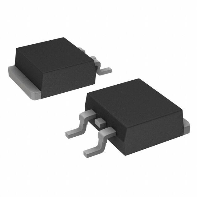
D2PAK
• Meets MSL level 1, per J-STD-020, LF maximum peak of
245 °C
2
(TO-263AB)
TO-262AA
3
Base
Common
Cathode
2
Base
Common
Cathode
2
2
Common
Cathode
2
Common
Cathode
3
Anode
1
Anode
DESCRIPTION / APPLICATIONS
Vishay Semiconductors 200 V series are the state of the art
hyperfast
recovery
rectifiers
designed
with
optimized performance of forward voltage drop and
hyperfast recovery time.
The planar structure and the platinum doped life
time control,
guarantee
the
best
overall
performance, ruggedness and reliability characteristics.
These devices are intended for use in the output rectification
stage of SMPS, UPS, DC/DC converters as well as
freewheeling diode in low voltage inverters and chopper
motor drives.
Their extremely optimized stored charge and low recovery
current minimize the switching losses and reduce over
dissipation in the switching element and snubbers.
3
Anode
1
Anode
VS-30CTH02S-M3
• Material categorization: for definitions of compliance
please see www.vishay.com/doc?99912
VS-30CTH02-1-M3
PRIMARY CHARACTERISTICS
IF(AV)
2 x 15 A
VR
200 V
VF at IF
0.78 V
trr typ.
30 ns
TJ max.
175 °C
Package
D2PAK (TO-263AB), TO-262AA
Circuit configuration
Common cathode
ABSOLUTE MAXIMUM RATINGS
PARAMETER
SYMBOL
Peak repetitive reverse voltage
TEST CONDITIONS
VRRM
per diode
Average rectified forward current
per device
Non-repetitive peak surge current
IF(AV)
IFSM
Operating junction and storage temperatures
TC = 159 °C
MAX.
UNITS
200
V
15
30
TC = 25 °C
TJ, TStg
A
200
-65 to +175
°C
ELECTRICAL SPECIFICATIONS (TJ = 25 °C unless otherwise specified)
PARAMETER
Breakdown voltage,
blocking voltage
SYMBOL
VBR, VR
Forward voltage
VF
Reverse leakage current
IR
Junction capacitance
CT
Series inductance
LS
TEST CONDITIONS
IR = 100 μA
MIN.
TYP.
MAX.
UNITS
200
-
-
V
IF = 15 A
-
0.92
1.05
IF = 15 A, TJ = 125 °C
-
0.78
0.85
VR = VR rated
-
-
10
TJ = 125 °C, VR = VR rated
-
5
300
VR = 200 V
-
57
-
pF
Measured lead to lead 5 mm from package body
-
8
-
nH
V
μA
Revision: 24-Oct-17
Document Number: 96234
1
For technical questions within your region: DiodesAmericas@vishay.com, DiodesAsia@vishay.com, DiodesEurope@vishay.com
THIS DOCUMENT IS SUBJECT TO CHANGE WITHOUT NOTICE. THE PRODUCTS DESCRIBED HEREIN AND THIS DOCUMENT
ARE SUBJECT TO SPECIFIC DISCLAIMERS, SET FORTH AT www.vishay.com/doc?91000
�VS-30CTH02S-M3, VS-30CTH02-1-M3
www.vishay.com
Vishay Semiconductors
DYNAMIC RECOVERY CHARACTERISTICS (TC = 25 °C unless otherwise specified)
PARAMETER
SYMBOL
Reverse recovery time
trr
TEST CONDITIONS
Reverse recovery charge
Qrr
MAX.
-
-
35
IF = 1 A, dIF/dt = 100 A/μs, VR = 30 V
-
-
30
TJ = 25 °C
-
26
-
-
40
-
TJ = 25 °C
IRRM
TYP.
IF = 1 A, dIF/dt = 50 A/μs, VR = 30 V
TJ = 125 °C
Peak recovery current
MIN.
IF = 15 A
dIF/dt = 200 A/μs
VR = 160 V
-
2.8
-
TJ = 125 °C
-
6.0
-
TJ = 25 °C
-
37
-
TJ = 125 °C
-
120
-
UNITS
ns
A
nC
THERMAL - MECHANICAL SPECIFICATIONS
PARAMETER
Maximum junction and storage temperature range
Thermal resistance, junction to case per diode
SYMBOL
MIN.
TYP.
MAX.
TJ, TStg
-65
-
175
°C
RthJC
-
-
1.1
°C/W
-
2.0
-
g
-
0.07
-
oz.
6.0
(5.0)
-
12
(10)
kgf · cm
(lbf · in)
Weight
Mounting torque
Marking device
UNITS
Case style D2PAK (TO-263AB)
30CTH02S
Case style TO-262
30CTH02-1
100
100
TJ = 175 °C
TJ = 125 °C
TJ = 25 °C
10
1
0.4
IR - Reverse Current (µA)
IF - Instantaneous Forward
Current (A)
TJ = 175 °C
TJ = 150 °C
10
TJ = 125 °C
1
TJ = 100 °C
TJ = 75 °C
0.1
TJ = 50 °C
0.01
TJ = 25 °C
0.001
0.0001
0.6
0.8
1.0
1.2
1.4
1.6
0
50
100
150
200
VFM - Forward Voltage Drop (V)
VR - Reverse Voltage (V)
Fig. 1 - Maximum Forward Voltage Drop Characteristics
Fig. 2 - Typical Values of Reverse Current vs.
Reverse Voltage
Revision: 24-Oct-17
Document Number: 96234
2
For technical questions within your region: DiodesAmericas@vishay.com, DiodesAsia@vishay.com, DiodesEurope@vishay.com
THIS DOCUMENT IS SUBJECT TO CHANGE WITHOUT NOTICE. THE PRODUCTS DESCRIBED HEREIN AND THIS DOCUMENT
ARE SUBJECT TO SPECIFIC DISCLAIMERS, SET FORTH AT www.vishay.com/doc?91000
�VS-30CTH02S-M3, VS-30CTH02-1-M3
www.vishay.com
Vishay Semiconductors
CT - Junction Capacitance (pF)
1000
100
TJ = 25 °C
10
0
50
100
150
200
ZthJC - Thermal Impedance (°C/W)
VR - Reverse Voltage (V)
Fig. 3 - Typical Junction Capacitance vs. Reverse Voltage
10
1
PDM
Single pulse
(thermal resistance)
0.01
0.00001
t1
D = 0.50
D = 0.20
D = 0.10
D = 0.05
D = 0.02
D = 0.01
0.1
0.0001
0.001
t2
Notes:
1. Duty factor D = t1/t2 .
2. Peak TJ = PDM x ZthJC + TC
0.01
0.1
1
.
10
t1 - Rectangular Pulse Duration (s)
Fig. 4 - Maximum Thermal Impedance ZthJC Characteristics
25
Average Power Loss (W)
Allowable Case Temperature (°C)
180
170
DC
160
Square wave (D = 0.50)
Rated VR applied
150
20
RMS limit
15
10
5
DC
See note (1)
140
D = 0.01
D = 0.02
D = 0.05
D = 0.1
D = 0.2
D = 0.5
0
0
5
10
15
20
25
0
5
10
15
20
25
IF(AV) - Average Forward Current (A)
IF(AV) - Average Forward Current (A)
Fig. 5 - Maximum Allowable Case Temperature vs.
Average Forward Current
Fig. 6 - Forward Power Loss Characteristics
Revision: 24-Oct-17
Document Number: 96234
3
For technical questions within your region: DiodesAmericas@vishay.com, DiodesAsia@vishay.com, DiodesEurope@vishay.com
THIS DOCUMENT IS SUBJECT TO CHANGE WITHOUT NOTICE. THE PRODUCTS DESCRIBED HEREIN AND THIS DOCUMENT
ARE SUBJECT TO SPECIFIC DISCLAIMERS, SET FORTH AT www.vishay.com/doc?91000
�VS-30CTH02S-M3, VS-30CTH02-1-M3
www.vishay.com
Vishay Semiconductors
100
1000
IF = 15 A
trr (ns)
Qrr (nC)
IF = 15 A
100
VR = 160 V
TJ = 125 °C
TJ = 25 °C
10
100
VR = 160 V
TJ = 125 °C
TJ = 25 °C
10
100
1000
1000
dIF/dt (A/µs)
dIF/dt (A/µs)
Fig. 7 - Typical Reverse Recovery Time vs. dIF/dt
Fig. 8 - Typical Stored Charge vs. dIF/dt
Note
Formula used: TC = TJ - (Pd + PdREV) x RthJC;
Pd = forward power loss = IF(AV) x VFM at (IF(AV)/D) (see fig. 6);
PdREV = inverse power loss = VR1 x IR (1 - D); IR at VR1 = rated VR
(1)
(3)
trr
IF
ta
tb
0
Qrr
(2)
IRRM
(4)
0.5 IRRM
di(rec)M/dt (5)
0.75 IRRM
(1) diF/dt
(1) diF/dt - rate of change of current
through zero crossing
(2) IRRM - peak reverse recovery current
(3) trr - reverse recovery time measured
from zero crossing point of negative
going IF to point where a line passing
through 0.75 IRRM and 0.50 IRRM
extrapolated to zero current.
(4) Qrr - area under curve defined by trr
and IRRM
Qrr =
trr x IRRM
2
(5) di(rec)M/dt - peak rate of change of
current during tb portion of trr
Fig. 9 - Reverse Recovery Waveform and Definitions
Revision: 24-Oct-17
Document Number: 96234
4
For technical questions within your region: DiodesAmericas@vishay.com, DiodesAsia@vishay.com, DiodesEurope@vishay.com
THIS DOCUMENT IS SUBJECT TO CHANGE WITHOUT NOTICE. THE PRODUCTS DESCRIBED HEREIN AND THIS DOCUMENT
ARE SUBJECT TO SPECIFIC DISCLAIMERS, SET FORTH AT www.vishay.com/doc?91000
�VS-30CTH02S-M3, VS-30CTH02-1-M3
www.vishay.com
Vishay Semiconductors
ORDERING INFORMATION TABLE
Device code
VS-
30
C
T
H
02
S
1
2
3
4
5
6
7
1
-
Vishay Semiconductors product
2
-
Current rating (30 A)
3
-
C = common cathode
4
-
T = TO-220, D2PAK
5
-
H = hyperfast rectifier
6
-
Voltage rating (02 = 200 V)
7
-
TRL -M3
8
9
S = D2PAK
-1 = TO-262
8
-
None = tube (50 pieces)
TRL = tape and reel (left oriented, for D2PAK package)
TRR = tape and reel (right oriented, for D2PAK package)
9
-
Environmental digit:
-M3 = halogen-free, RoHS-compliant, and terminations lead (Pb)-free
LINKS TO RELATED DOCUMENTS
Dimensions
Part marking information
Packaging information
D2PAK
www.vishay.com/doc?96164
TO-262AA
www.vishay.com/doc?96165
D2PAK
www.vishay.com/doc?95444
TO-262AA
www.vishay.com/doc?95443
www.vishay.com/doc?96424
Revision: 24-Oct-17
Document Number: 96234
5
For technical questions within your region: DiodesAmericas@vishay.com, DiodesAsia@vishay.com, DiodesEurope@vishay.com
THIS DOCUMENT IS SUBJECT TO CHANGE WITHOUT NOTICE. THE PRODUCTS DESCRIBED HEREIN AND THIS DOCUMENT
ARE SUBJECT TO SPECIFIC DISCLAIMERS, SET FORTH AT www.vishay.com/doc?91000
�Outline Dimensions
www.vishay.com
Vishay Semiconductors
D2PAK
DIMENSIONS in millimeters and inches
Conforms to JEDEC® outline D2 PAK (SMD-220)
(2)(3)
E
B
Pad layout
A
A
(E)
c2
11.00
MIN.
(0.43)
A
(3) L1
4
9.65
MIN.
(0.38)
(D1) (3)
Detail A
D
H
1
2
17.90 (0.70)
15.00 (0.625)
(2)
3
3.81
MIN.
(0.15)
L2
B
B
2.32
MIN.
(0.08)
A
2 x b2
C
2xb
2.64 (0.103)
2.41 (0.096)
(3)
E1
c
View A - A
± 0.004 M B
0.010 M A M B
2x e
Plating
Base
Metal
(4)
b1, b3
H
Gauge
plane
L
Seating
plane
L3
A1
Lead tip
(b, b2)
L4
Section B - B and C - C
Scale: None
Detail “A”
Rotated 90 °CW
Scale: 8:1
SYMBOL
MILLIMETERS
MIN.
MAX.
INCHES
MIN.
c1 (4)
(c)
B
0° to 8°
MAX.
NOTES
SYMBOL
MILLIMETERS
MIN.
MAX.
INCHES
MIN.
MAX.
NOTES
A
4.06
4.83
0.160
0.190
D1
6.86
8.00
0.270
0.315
3
A1
0.00
0.254
0.000
0.010
E
9.65
10.67
0.380
0.420
2, 3
E1
7.90
8.80
0.311
0.346
3
b
0.51
0.99
0.020
0.039
b1
0.51
0.89
0.020
0.035
b2
1.14
1.78
0.045
0.070
b3
1.14
1.73
0.045
0.068
c
0.38
0.74
0.015
0.029
c1
0.38
0.58
0.015
0.023
c2
1.14
1.65
0.045
0.065
D
8.51
9.65
0.335
0.380
4
4
e
2.54 BSC
0.100 BSC
H
14.61
15.88
0.575
0.625
0.110
L
1.78
2.79
0.070
L1
-
1.65
-
0.066
4
L2
1.27
1.78
0.050
0.070
2
L4
L3
0.25 BSC
4.78
5.28
3
0.010 BSC
0.188
0.208
Notes
(1) Dimensioning and tolerancing per ASME Y14.5 M-1994
(2) Dimension D and E do not include mold flash. Mold flash shall not exceed 0.127 mm (0.005") per side. These dimensions are measured at
the outmost extremes of the plastic body
(3) Thermal pad contour optional within dimension E, L1, D1 and E1
(4) Dimension b1 and c1 apply to base metal only
(5) Datum A and B to be determined at datum plane H
(6) Controlling dimension: inches
(7) Outline conforms to JEDEC® outline TO-263AB
Revision: 13-Jul-17
Document Number: 96164
1
For technical questions within your region: DiodesAmericas@vishay.com, DiodesAsia@vishay.com, DiodesEurope@vishay.com
THIS DOCUMENT IS SUBJECT TO CHANGE WITHOUT NOTICE. THE PRODUCTS DESCRIBED HEREIN AND THIS DOCUMENT
ARE SUBJECT TO SPECIFIC DISCLAIMERS, SET FORTH AT www.vishay.com/doc?91000
�Legal Disclaimer Notice
www.vishay.com
Vishay
Disclaimer
ALL PRODUCT, PRODUCT SPECIFICATIONS AND DATA ARE SUBJECT TO CHANGE WITHOUT NOTICE TO IMPROVE
RELIABILITY, FUNCTION OR DESIGN OR OTHERWISE.
Vishay Intertechnology, Inc., its affiliates, agents, and employees, and all persons acting on its or their behalf (collectively,
“Vishay”), disclaim any and all liability for any errors, inaccuracies or incompleteness contained in any datasheet or in any other
disclosure relating to any product.
Vishay makes no warranty, representation or guarantee regarding the suitability of the products for any particular purpose or
the continuing production of any product. To the maximum extent permitted by applicable law, Vishay disclaims (i) any and all
liability arising out of the application or use of any product, (ii) any and all liability, including without limitation special,
consequential or incidental damages, and (iii) any and all implied warranties, including warranties of fitness for particular
purpose, non-infringement and merchantability.
Statements regarding the suitability of products for certain types of applications are based on Vishay's knowledge of typical
requirements that are often placed on Vishay products in generic applications. Such statements are not binding statements
about the suitability of products for a particular application. It is the customer's responsibility to validate that a particular product
with the properties described in the product specification is suitable for use in a particular application. Parameters provided in
datasheets and / or specifications may vary in different applications and performance may vary over time. All operating
parameters, including typical parameters, must be validated for each customer application by the customer's technical experts.
Product specifications do not expand or otherwise modify Vishay's terms and conditions of purchase, including but not limited
to the warranty expressed therein.
Hyperlinks included in this datasheet may direct users to third-party websites. These links are provided as a convenience and
for informational purposes only. Inclusion of these hyperlinks does not constitute an endorsement or an approval by Vishay of
any of the products, services or opinions of the corporation, organization or individual associated with the third-party website.
Vishay disclaims any and all liability and bears no responsibility for the accuracy, legality or content of the third-party website
or for that of subsequent links.
Except as expressly indicated in writing, Vishay products are not designed for use in medical, life-saving, or life-sustaining
applications or for any other application in which the failure of the Vishay product could result in personal injury or death.
Customers using or selling Vishay products not expressly indicated for use in such applications do so at their own risk. Please
contact authorized Vishay personnel to obtain written terms and conditions regarding products designed for such applications.
No license, express or implied, by estoppel or otherwise, to any intellectual property rights is granted by this document or by
any conduct of Vishay. Product names and markings noted herein may be trademarks of their respective owners.
© 2021 VISHAY INTERTECHNOLOGY, INC. ALL RIGHTS RESERVED
Revision: 09-Jul-2021
1
Document Number: 91000
�