VS-50TPS12LHM3
www.vishay.com
Vishay Semiconductors
Thyristor High Voltage, Phase Control SCR, 50 A
FEATURES
2
(A)
• AEC-Q101 qualified, meets JESD 201
class 1A whisker test
• Flexible solution for reliable AC power
rectification
1
2
• Easy control peak current at charger power
up to reduce passive / electromechanical components
3
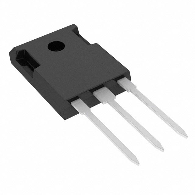
TO-247AD 3L
1 (K)
(G) 3
• Material categorization: for definitions of compliance
please see www.vishay.com/doc?99912
APPLICATIONS
PRIMARY CHARACTERISTICS
IT(AV)
50 A
VDRM/VRRM
1200 V
VTM (typ.)
1.2 V
IGT (typ.)
45 mA
• On-board and off-board EV / HEV battery chargers
• Renewable energy inverters
DESCRIPTION
TJ max.
150 °C
Package
TO-247AD 3L
Circuit configuration
Single SCR
The VS-50TPS12 high voltage series of silicon controlled
rectifiers are specifically designed for medium power
switching, and phase control applications.
MAJOR RATINGS AND CHARACTERISTICS
PARAMETER
SYMBOL
Peak repetitive reverse voltage
VRRM / VDRM
On-state voltage
VT
TEST CONDITIONS
VALUES
50 A, TJ = 125 °C
Average rectified forward current
IT(AV)
IRMS
79
Non-repetitive peak surge current
ITSM
630
Operating junction and storage temperature range
V
1.2
Maximum continuous RMS on-state current
Maximum rate of rise
UNITS
1200
50
A
dv/dt
1000
V/μs
TJ, TStg
-40 to +150
°C
VOLTAGE RATINGS
PART NUMBER
VS-50TPS12LHM3
VRRM / VDRM, MAXIMUM
REPETITIVE PEAK AND
OFF-STATE VOLTAGE
V
VRSM, MAXIMUM
NON-REPETITIVE PEAK
REVERSE VOLTAGE
V
IRRM / IDRM
AT 150 °C
mA
1200
1300
70
Revision: 27-Jul-2018
Document Number: 96108
1
For technical questions within your region: DiodesAmericas@vishay.com, DiodesAsia@vishay.com, DiodesEurope@vishay.com
THIS DOCUMENT IS SUBJECT TO CHANGE WITHOUT NOTICE. THE PRODUCTS DESCRIBED HEREIN AND THIS DOCUMENT
ARE SUBJECT TO SPECIFIC DISCLAIMERS, SET FORTH AT www.vishay.com/doc?91000
�VS-50TPS12LHM3
www.vishay.com
Vishay Semiconductors
ABSOLUTE MAXIMUM RATINGS
PARAMETER
Maximum average on-state current
Maximum continuous RMS on-state
current as AC switch
Peak, one-cycle non-repetitive surge current
SYMBOL
IT(AV)
TEST CONDITIONS
TYP.
TC = 112 °C, 180° conduction half sine wave
IT(RMS)
ITSM
I2t for fusing
I2t
I2t for fusing
I2t
10 ms sine pulse, rated VRRM applied
10 ms sine pulse, no voltage reapplied
MAX. UNITS
-
50
-
79
-
530
-
630
-
1405
10 ms sine pulse, no voltage reapplied
-
1986
t = 0.1 ms to 10 ms, no voltage reapplied, TJ = 125 °C
-
19 850
10 ms sine pulse, rated VRRM applied
Initial TJ = TJ
maximum
Low level value of threshold voltage
VT(TO)1
-
0.89
High level value of threshold voltage
VT(TO)2
-
0.97
-
6.77
-
6.32
50 A, TJ = 25 °C
1.2
1.32
100 A, TJ = 25 °C
1.4
1.6
-
150
-
300
Low level value of on-state slope resistance
rt1
High level value of on-state slope resistance
rt2
On-state voltage
VT
Rate of rise of turned-on current
di/dt
Holding current
IH
Latching current
IL
Reverse and direct leakage current
Rate of rise of off-state voltage
IRRM/IDRM
dv/dt
TJ = 125 °C
TJ = 25 °C
Anode supply = 6 V, resistive load, TJ = 25 °C
TJ = 25 °C
-
350
-
0.05
A
A2s
A2s
V
m
V
A/μs
mA
TJ = 150 °C
-
70
TJ = TJ maximum, linear to 80 % VDRM, Rg-k = 100
-
1000
V/μs
TYP.
MAX.
UNITS
-
10
-
2.5
-
2.5
TRIGGERING
PARAMETER
Peak gate power
Average gate power
Peak gate current
Peak negative gate voltage
SYMBOL
PGM
PG(AV)
TEST CONDITIONS
10 ms sine pulse, no voltage reapplied
IGM
-VGM
TJ = -40 °C
Required DC gate voltage to trigger
Required DC gate to trigger
VGT
IGT
TJ = 25 °C
Anode supply = 6 V resistive load
VGD
DC gate current not to trigger
IGD
10
1.6
-
1.5
A
V
TJ = 150 °C
-
1
TJ = -40 °C
-
160
45
100
-
60
-
0.2
V
-
3
mA
UNITS
TJ = 25 °C
Anode supply = 6 V resistive load
TJ = 150 °C
DC gate voltage not to trigger
-
W
TJ = 150 °C, VDRM = rated value
mA
SWITCHING
PARAMETER
SYMBOL
TYP.
MAX.
Turn-on time
tgt
IT = 50 A, VD = 50 % VDRM, Igt = 300 mA, TJ = 25 °C
TEST CONDITIONS
1.5
-
Turn-off time
tq
IT = 50 A, VD = 80 % VDRM, dV/dt = 20 V/μs, tp = 200 μs
Igt = 100 mA, dI/dt = 10 A/μs, VR = 100 V, TJ = 150 °C
92
-
μs
Revision: 27-Jul-2018
Document Number: 96108
2
For technical questions within your region: DiodesAmericas@vishay.com, DiodesAsia@vishay.com, DiodesEurope@vishay.com
THIS DOCUMENT IS SUBJECT TO CHANGE WITHOUT NOTICE. THE PRODUCTS DESCRIBED HEREIN AND THIS DOCUMENT
ARE SUBJECT TO SPECIFIC DISCLAIMERS, SET FORTH AT www.vishay.com/doc?91000
�VS-50TPS12LHM3
www.vishay.com
Vishay Semiconductors
THERMAL AND MECHANICAL SPECIFICATIONS
PARAMETER
SYMBOL
Maximum junction and storage temperature range
TYP.
MAX.
UNITS
TJ, TStg
-40
150
°C
RthJC
-
0.35
-
40
0.2
-
Maximum thermal resistance, junction to case
Maximum thermal resistance, junction to ambient
RthJA
Typical thermal resistance, case to heatsink
RthCS
Mounting torque
TEST CONDITIONS
Mounting surface, smooth, and greased
minimum
6 (5)
maximum
12 (10)
Marking device
Case style Super TO-247AD 3L
°C/W
kgf · cm
(lbf · in)
50TPS12LH
RthJ-HS CONDUCTION PER JUNCTION
SINE HALF-WAVE CONDUCTION
Maximum Allowable Case Temperature ( °C)
VS-50TPS12LHM3
120°
90°
60°
30°
180°
120°
90°
60°
30°
0.143
0.166
0.208
0.299
0.490
0.099
0.168
0.223
0.311
0.494
150
RthJC (DC) = 0.35 °C/W
140
30°
Ø
60°
130
Conduction Angle
90°
120
120°
110
180°
100
90
0
10
RECTANGULAR WAVE CONDUCTION
180°
20
30
40
50
60
Max. Average On-state Power Loss (W)
DEVICE
70
60
50
RMS limit
40
30
Ø
20
Conduction Angle
10
Tj = 150 °C
0
0
RthJC (DC) = 0.35 °C/W
DC°
Ø
Conduction Angle
60°
120
90°
120°
110
180°
100
90
0
10
20
30
40
50
60
70
20
30
40
50
60
Fig. 3 - On-State Power Loss Characteristics
150
30°
10
Average On-state Current (A)
80
Max. Average On-state Power Loss (W)
Maximum Allowable Case Temperature (°C)
180°
120°
90°
60°
30°
80
Fig. 1 - Current Rating Characteristics
130
°C/W
90
Average On - State Current (A)
140
UNITS
110
180°
120°
90°
60°
30°
100
90
80
DC
70
60
RMS limit
50
40
Ø
30
Conduction Angle
20
10
Tj = 150 °C
0
0
10
20
30
40
50
60
70
80
Average On - state Current (A)
Average On-state Current (A)
Fig. 2 - Current Rating Characteristics
Fig. 4 - On-State Power Loss Characteristics
Revision: 27-Jul-2018
Document Number: 96108
3
For technical questions within your region: DiodesAmericas@vishay.com, DiodesAsia@vishay.com, DiodesEurope@vishay.com
THIS DOCUMENT IS SUBJECT TO CHANGE WITHOUT NOTICE. THE PRODUCTS DESCRIBED HEREIN AND THIS DOCUMENT
ARE SUBJECT TO SPECIFIC DISCLAIMERS, SET FORTH AT www.vishay.com/doc?91000
�VS-50TPS12LHM3
Vishay Semiconductors
Peak Half Sine Wave On- state Current (A)
Peak Half Sine Wave On - state Current (A)
www.vishay.com
560
At any rated load condition and with
rated VRRM applied following surge.
Initial Tj = 150 °C
at 60 Hz 0.0083 s
at 50 Hz 0.0100 s
510
460
410
360
310
260
1
10
100
Number Of Equal Amplitude
Half Cycle Current Pulse (N)
650
550
500
450
400
350
300
250
0.01
0.1
1
Number Of Equal Amplitude
Half Cycle Current Pulse (N)
Fig. 5 - Maximum Non-Repetitive Surge Current
Instantaneous On - state Current (A)
Maximum non repetitive surge current
vs. pulse train duration. Control of
conduction may not be maintained.
Initial Tj = 150 °C
No voltage reapplied
rated VRRM reapplied
600
Fig. 6 - Maximum Non-Repetitive Surge Current
1000
100
TJ = 125 °C
10
TJ = 25 °C
1
0.5
1.0
1.5
2.0
2.5
3.0
Instantaneous On - state Voltage (V)
Fig. 7 - On-State Voltage Drop Characteristics
Rectangular gate pulse
a) Recommended load line for rated dI/dt: 20 V, 30 Ω
tr = 0.5 μs, tp ≥ 6 μs
b) Recommended load line for ≤ 30 % rated dI/dt: 20 V, 65 Ω
tr = 1 μs, tp ≥ 6 μs
(1) PGM = 100 W, tp = 500 μs
(2) PGM = 50 W, tp = 1 ms
(3) PGM = 20 W, tp = 2.5 ms
(4) PGM = 10 W, tp = 5 ms
10
VGD
0.1
0.0001
IGD
0.001
50TPS12L Series
0.01
0.1
TJ = - 40 °C
1
TJ = 25 °C
TJ = 150 °C
Instantaneous Gate Voltage (V)
100
(4)
b)
a)
(3)
(2)
(1)
Frequency limited by PG(AV)
1
10
100
1000
Instantaneous Gate Current (A)
Fig. 8 - Gate Characteristics
Revision: 27-Jul-2018
Document Number: 96108
4
For technical questions within your region: DiodesAmericas@vishay.com, DiodesAsia@vishay.com, DiodesEurope@vishay.com
THIS DOCUMENT IS SUBJECT TO CHANGE WITHOUT NOTICE. THE PRODUCTS DESCRIBED HEREIN AND THIS DOCUMENT
ARE SUBJECT TO SPECIFIC DISCLAIMERS, SET FORTH AT www.vishay.com/doc?91000
�VS-50TPS12LHM3
ZthJC - Transient Thermal Impedance
(°C/W)
www.vishay.com
Vishay Semiconductors
1
0.50
0.1
0.33
0.25
0.17
0.08
Single Pulse
0.01
0.0001
0.001
0.01
0.1
1
10
Square Wave Pulse Duration (s)
Fig. 9 - Thermal Impedance ZthJC Characteristics
ORDERING INFORMATION TABLE
Device code
VS-
50
T
P
S
12
L
H
M3
1
2
3
4
5
6
7
8
9
1
-
Vishay Semiconductors product
2
-
Current code (50 = 50 A)
3
-
Circuit configuration:
T = thyristor
4
-
P = TO-247AD package
5
-
Type of silicon:
6
-
Voltage code (12 = 1200 V)
7
-
Package L = long lead
8
-
H = AEC-Q101 qualified
9
-
M3 = halogen-free, RoHS-compliant, and terminations lead (Pb)-free
S = standard recovery rectifier
ORDERING INFORMATION (example)
PREFERRED P/N
QUANTITY PER TUBE
MINIMUM ORDER QUANTITY
PACKAGING DESCRIPTION
VS-50TPS12LHM3
25
contact factory
Antistatic plastic tubes
LINKS TO RELATED DOCUMENTS
Dimensions
TO-247AD 3L
www.vishay.com/doc?95626
Part marking information
TO-247AD 3L
www.vishay.com/doc?95007
Revision: 27-Jul-2018
Document Number: 96108
5
For technical questions within your region: DiodesAmericas@vishay.com, DiodesAsia@vishay.com, DiodesEurope@vishay.com
THIS DOCUMENT IS SUBJECT TO CHANGE WITHOUT NOTICE. THE PRODUCTS DESCRIBED HEREIN AND THIS DOCUMENT
ARE SUBJECT TO SPECIFIC DISCLAIMERS, SET FORTH AT www.vishay.com/doc?91000
�Outline Dimensions
www.vishay.com
Vishay Semiconductors
TO-247AD 3L
DIMENSIONS in millimeters and inches
A
A
(3)
(6) Φ P
E
B
(2) R/2
A2
S
(Datum B)
Ø K M DBM
Φ P1
A
D2
Q
2xR
(2)
D1 (4)
D
1
4
D
3
2
Thermal pad
(5) L1
C
L
(4)
E1
A
0.01 M D B M
View A - A
See view B
2 x b2
3xb
C
2x e
b4
A1
0.10 M C A M
(b1, b3, b5)
Plating
Base metal
D DE
(c)
c1
E
C
C
(b, b2, b4)
(4)
Section C - C, D - D, E - E
SYMBOL
A
A1
A2
b
b1
b2
b3
b4
b5
c
c1
D
D1
MILLIMETERS
MIN.
MAX.
4.65
5.31
2.21
2.59
1.50
2.49
0.99
1.40
0.99
1.35
1.65
2.39
1.65
2.34
2.59
3.43
2.59
3.38
0.38
0.89
0.38
0.84
19.71
20.70
13.08
-
INCHES
MIN.
MAX.
0.183
0.209
0.087
0.102
0.059
0.098
0.039
0.055
0.039
0.053
0.065
0.094
0.065
0.092
0.102
0.135
0.102
0.133
0.015
0.035
0.015
0.033
0.776
0.815
0.515
-
View B
NOTES
3
4
SYMBOL
D2
E
E1
e
ØK
L
L1
ØP
Ø P1
Q
R
S
MILLIMETERS
MIN.
MAX.
0.51
1.30
15.29
15.87
13.46
5.46 BSC
0.254
19.81
20.32
3.71
4.29
3.56
3.66
6.98
5.31
5.69
4.52
5.49
5.51 BSC
INCHES
MIN.
MAX.
0.020
0.051
0.602
0.625
0.53
0.215 BSC
0.010
0.780
0.800
0.146
0.169
0.14
0.144
0.275
0.209
0.224
0.178
0.216
0.217 BSC
NOTES
3
Notes
(1) Dimensioning and tolerancing per ASME Y14.5M-1994
(2) Contour of slot optional
(3) Dimension D and E do not include mold flash. These dimensions are measured at the outermost extremes of the plastic body
(4) Thermal pad contour optional with dimensions D1 and E1
(5) Lead finish uncontrolled in L1
(6) Ø P to have a maximum draft angle of 1.5 to the top of the part with a maximum hole diameter of 3.91 mm (0.154")
(7) Outline conforms to JEDEC® outline TO-247 with exception of dimension A min., D, E min., Q min., S, and note 4
Revision: 06-Mar-2020
Document Number: 95626
1
For technical questions within your region: DiodesAmericas@vishay.com, DiodesAsia@vishay.com, DiodesEurope@vishay.com
THIS DOCUMENT IS SUBJECT TO CHANGE WITHOUT NOTICE. THE PRODUCTS DESCRIBED HEREIN AND THIS DOCUMENT
ARE SUBJECT TO SPECIFIC DISCLAIMERS, SET FORTH AT www.vishay.com/doc?91000
�Legal Disclaimer Notice
www.vishay.com
Vishay
Disclaimer
ALL PRODUCT, PRODUCT SPECIFICATIONS AND DATA ARE SUBJECT TO CHANGE WITHOUT NOTICE TO IMPROVE
RELIABILITY, FUNCTION OR DESIGN OR OTHERWISE.
Vishay Intertechnology, Inc., its affiliates, agents, and employees, and all persons acting on its or their behalf (collectively,
“Vishay”), disclaim any and all liability for any errors, inaccuracies or incompleteness contained in any datasheet or in any other
disclosure relating to any product.
Vishay makes no warranty, representation or guarantee regarding the suitability of the products for any particular purpose or
the continuing production of any product. To the maximum extent permitted by applicable law, Vishay disclaims (i) any and all
liability arising out of the application or use of any product, (ii) any and all liability, including without limitation special,
consequential or incidental damages, and (iii) any and all implied warranties, including warranties of fitness for particular
purpose, non-infringement and merchantability.
Statements regarding the suitability of products for certain types of applications are based on Vishay's knowledge of typical
requirements that are often placed on Vishay products in generic applications. Such statements are not binding statements
about the suitability of products for a particular application. It is the customer's responsibility to validate that a particular product
with the properties described in the product specification is suitable for use in a particular application. Parameters provided in
datasheets and / or specifications may vary in different applications and performance may vary over time. All operating
parameters, including typical parameters, must be validated for each customer application by the customer's technical experts.
Product specifications do not expand or otherwise modify Vishay's terms and conditions of purchase, including but not limited
to the warranty expressed therein.
Hyperlinks included in this datasheet may direct users to third-party websites. These links are provided as a convenience and
for informational purposes only. Inclusion of these hyperlinks does not constitute an endorsement or an approval by Vishay of
any of the products, services or opinions of the corporation, organization or individual associated with the third-party website.
Vishay disclaims any and all liability and bears no responsibility for the accuracy, legality or content of the third-party website
or for that of subsequent links.
Except as expressly indicated in writing, Vishay products are not designed for use in medical, life-saving, or life-sustaining
applications or for any other application in which the failure of the Vishay product could result in personal injury or death.
Customers using or selling Vishay products not expressly indicated for use in such applications do so at their own risk. Please
contact authorized Vishay personnel to obtain written terms and conditions regarding products designed for such applications.
No license, express or implied, by estoppel or otherwise, to any intellectual property rights is granted by this document or by
any conduct of Vishay. Product names and markings noted herein may be trademarks of their respective owners.
© 2021 VISHAY INTERTECHNOLOGY, INC. ALL RIGHTS RESERVED
Revision: 09-Jul-2021
1
Document Number: 91000
�