VSKDL240, VSKCL240, VSKJL240, VSKEL240 Series
www.vishay.com
Vishay Semiconductors
Fast Recovery Diodes, 250 A
(MAGN-A-PAK Power Modules)
FEATURES
• Fast recovery time characteristics
• Electrically isolated base plate
• Industrial standard package
• Simplified mechanical designs, rapid assembly
• High surge capability
• Large creepage distances
• 3000 VRMS isolating voltage
• UL approved file E78996
• Compliant to RoHS Directive 2002/95/EC
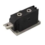
MAGN-A-PAK
• Designed and qualified for industrial level
DESCRIPTION
PRODUCT SUMMARY
IF(AV)
250 A
Type
Modules - Diode, Fast
The VSK.L240 Series of MAGN-A-PAKs uses fast recovery
power diodes in four basic configurations. The
semiconductors are electrically isolated from the metal
base, allowing common heatsinks and compact assemblies
to be built. Application includes power supplies, battery
chargers, welders, motor controls and general industrial
current rectification. These modules are intended for those
applications where fast recovery characteristics are
required.
MAJOR RATINGS AND CHARACTERISTICS
SYMBOL
IF(AV)
CHARACTERISTICS
I2t
UNITS
S10/S20
S30
250
240
A
TC
100
100
°C
392
377
50 Hz
8000
7500
60 Hz
8400
7850
50 Hz
322
280
60 Hz
294
256
3220
2800
IF(RMS)
IFSM
VSK.L240
I2t
A
kA2s
kA2s
VRRM
Range
600 to 2500
V
TJ
Range
- 40 to 150
°C
Revision: 07-Oct-11
Document Number: 93164
1
For technical questions within your region: DiodesAmericas@vishay.com, DiodesAsia@vishay.com, DiodesEurope@vishay.com
THIS DOCUMENT IS SUBJECT TO CHANGE WITHOUT NOTICE. THE PRODUCTS DESCRIBED HEREIN AND THIS DOCUMENT
ARE SUBJECT TO SPECIFIC DISCLAIMERS, SET FORTH AT www.vishay.com/doc?91000
�VSKDL240, VSKCL240, VSKJL240, VSKEL240 Series
www.vishay.com
Vishay Semiconductors
ELECTRICAL SPECIFICATIONS
VOLTAGE RATINGS
TYPE NUMBER
VOLTAGE
CODE
trr
CODE
VRRM, MAXIMUM REPETITIVE
PEAK REVERSE VOLTAGE
V
VRSM, MAXIMUM
NON-REPETITIVE PEAK
REVERSE VOLTAGE
V
06
S10
600
700
10
S10
1000
1100
12
S20
1200
1300
14
S20
1400
1500
20
S30
2000
2100
25
S30
2500
2600
VSK.L240
IRRM MAXIMUM
AT 150 °C
mA
50
FORWARD CONDUCTION
PARAMETER
Maximum average forward current
at case temperature
Maximum RMS forward current
Maximum peak, one-cycle forward
non-repetitive, surge current
SYMBOL
IF(AV)
IF(RMS)
IFSM
TEST CONDITIONS
180° conduction, half sine wave
I2t
240
A
100
100
°C
392
377
7500
8400
7850
6750
6300
7100
6600
322
280
294
256
228
198
t = 8.3 ms
t = 10 ms
t = 8.3 ms
t = 10 ms
t = 8.3 ms
Maximum I2t for fusing
250
8000
t = 10 ms
I2t
S30
t = 10 ms
No voltage
reapplied
100 % VRRM
reapplied
No voltage
reapplied
Sinusoidal half wave,
initial TJ = TJ maximum
100 % VRRM
reapplied
208
181
t = 0.1 ms to 10 ms, no voltage reapplied
3220
2800
Low level value of threshold voltage
VF(TO)1
(16.7 % x x IF(AV) < I < x IF(AV)),
TJ = TJ maximum
0.98
0.98
High level value of threshold voltage
VF(TO)2
(I > x IF(AV)), TJ = TJ maximum
1.31
1.31
Low level value of forward slope resistance
rf1
(16.7 % x x IF(AV) < I < x IF(AV)),
TJ = TJ maximum
0.75
0.97
High level value of forward slope resistance
rf2
(I > x IF(AV)), TJ = TJ maximum
0.41
0.60
IFM = 800 A, TJ = 150 °C, tp = 10 ms
Average power = VF(TO) x IF(AV) + rf x (IF(RMS))2
1.57
1.75
Maximum forward voltage drop
Revision: 07-Oct-11
VFM
UNITS
S10/S20
As AC switch
t = 8.3 ms
Maximum I2t for fusing
VSK.L240
A
kA2s
kA2s
V
m
V
Document Number: 93164
2
For technical questions within your region: DiodesAmericas@vishay.com, DiodesAsia@vishay.com, DiodesEurope@vishay.com
THIS DOCUMENT IS SUBJECT TO CHANGE WITHOUT NOTICE. THE PRODUCTS DESCRIBED HEREIN AND THIS DOCUMENT
ARE SUBJECT TO SPECIFIC DISCLAIMERS, SET FORTH AT www.vishay.com/doc?91000
�VSKDL240, VSKCL240, VSKJL240, VSKEL240 Series
www.vishay.com
Vishay Semiconductors
RECOVERY CHARACTERISTICS
MAXIMUM VALUE
AT TJ = 25 °C
CODE
trr AT 25 % IRRM
(μs)
S10
1.0
S20
2.0
S30
3.0
TYPICAL VALUES
AT TJ = 150 °C
TEST CONDITIONS
Ipk
SQUARE PULSE
(A)
500
dI/dt
(A/μs)
100
Vr
(V)
trr
AT 25 % IRRM
(μs)
Qrr
(μC)
Ir
(A)
IFM
2.7
135
100
di
dt
3.5
250
145
3.6
360
200
- 50
trr
t
Qrr
IRM(REC)
BLOCKING
PARAMETER
SYMBOL
Maximum peak reverse leakage current
RMS insulation voltage
TEST CONDITIONS
IRRM
TJ = 150 °C, leakage current
VINS
50 Hz, circuit to base, all terminals shorted,
25 °C, t = 1 s
VALUES
UNITS
50
mA
3000
V
THERMAL AND MECHANICAL SPECIFICATIONS
PARAMETER
SYMBOL
Maximum junction operating and
storage temperature range
TEST CONDITIONS
TJ, TStg
VALUES
UNITS
- 40 to 150
°C
Maximum internal thermal resistance,
junction to case per junction
RthJC
DC operation
0.125
Thermal resistance,
case to heatsink per module
RthCS
Mounting surface flat, smooth and greased
0.02
K/W
MAP to heatsink
Mounting torque ± 10 %
busbar to MAP
A mounting compound is recommended
and the torque should be rechecked after a
period of about 3 hours to allow for the
spread of the compound.
Approximate weight
Case style
4 to 6
Nm
8 to 10
850
g
30
oz.
MAGN-A-PAK
R CONDUCTION PER JUNCTION
CONDUCTION ANGLE
SINUSOIDAL CONDUCTION
RECTANGULAR CONDUCTION
180°
0.008
0.007
120°
0.010
0.011
90°
0.013
0.015
60°
0.019
0.020
30°
0.032
0.033
TEST CONDITIONS
UNITS
TJ = TJ maximum
K/W
Note
• The table above shows the increment of thermal resistance RthJC when devices operate at different conduction angles than DC
Revision: 07-Oct-11
Document Number: 93164
3
For technical questions within your region: DiodesAmericas@vishay.com, DiodesAsia@vishay.com, DiodesEurope@vishay.com
THIS DOCUMENT IS SUBJECT TO CHANGE WITHOUT NOTICE. THE PRODUCTS DESCRIBED HEREIN AND THIS DOCUMENT
ARE SUBJECT TO SPECIFIC DISCLAIMERS, SET FORTH AT www.vishay.com/doc?91000
�VSKDL240, VSKCL240, VSKJL240, VSKEL240 Series
Vishay Semiconductors
150
VSK.L240..S10/ S20 Series
R thJC (DC) = 0.125 K/ W
140
130
Conduction Angle
120
110
30°
100
60°
90°
120°
90
180°
80
0
50
100
150
200
250
300
Maximum Average Forward Pow er Loss (W)
Maximum Allowable Case Temperature (°C)
www.vishay.com
600
DC
180°
120°
90°
60°
30°
500
400
300
RMS Limit
200
Conduction Period
100
VSK.L240..S10/ S20 Series
TJ = 150°C Per Junc tion
0
0
50
Average Forward Current (A)
Fig. 4 - Forward Power Loss Characteristics
150
VSK.L240..S10/ S20 Series
R thJC(DC) = 0.125 K/ W
130
120
Conduction Period
110
30°
60°
100
90°
120°
90
180°
DC
80
0
Peak Half Sine Wave Forward Current (A)
Maximum Allowable Case Temperature (°C)
Fig. 1 - Current Ratings Characteristics
140
At Any Rated Load Condition And With
Rated VRRM App lied Following Surge.
7000
Initial T J= 150°C
@ 60 Hz 0.0083 s
@ 50 Hz 0.0100 s
6000
5000
4000
3000
VSK.L240..S10/ S20 Series
Per Junc tion
2000
1
Average Forward Current (A)
180°
120°
90°
60°
30°
250
RMS Limit
200
150
Conduction Angle
100
VSK.L240..S10/ S20 Series
Per Junc tion TJ = 150°C
50
0
0
50
100
150
200
100
Fig. 5 - Maximum Non-Repetitive Surge Current
Peak Half Sine Wave Forward Current (A)
400
300
10
Number Of Equa l Amplitude Half Cyc le Current Pulses (N)
Fig. 2 - Current Ratings Characteristics
Maximum Average Forward Power Loss (W)
8000
50 100 150 200 250 300 350 400 450
350
100 150 200 250 300 350 400
Average Forward Current (A)
250
8500
Maximum Non Repetitive Surge Current
Versus Pulse Train Dura tion.
Initial T J = 150°C
No Vo ltage Reap plied
Rated V RRMReap plied
7500
6500
5500
4500
3500
2500
VSK.L240..S10/ S20 Series
Per Junction
1500
0.01
0.1
1
Average Forward Current (A)
Pulse Train Dura tion (s)
Fig. 3 - Forward Power Loss Characteristics
Fig. 6 - Maximum Non-Repetitive Surge Current
Revision: 07-Oct-11
Document Number: 93164
4
For technical questions within your region: DiodesAmericas@vishay.com, DiodesAsia@vishay.com, DiodesEurope@vishay.com
THIS DOCUMENT IS SUBJECT TO CHANGE WITHOUT NOTICE. THE PRODUCTS DESCRIBED HEREIN AND THIS DOCUMENT
ARE SUBJECT TO SPECIFIC DISCLAIMERS, SET FORTH AT www.vishay.com/doc?91000
�VSKDL240, VSKCL240, VSKJL240, VSKEL240 Series
150
VSK.L240..S30 Series
RthJC(DC) = 0.125 K/ W
140
130
Conduction Angle
120
110
30°
100
60°
90°
90
120°
180°
80
0
50
100
150
200
250
Maximum Averag e Forward Power Loss (W)
Vishay Semiconductors
DC
180°
120°
90°
60°
30°
500
450
400
350
300
250 RMS Limit
200
Cond uc tion Period
150
VSK.L240..S30 Series
Per Junc tion
TJ = 150°C
100
50
0
0
50
100 150 200 250 300 350 400
Average Forward Current (A)
Average Forward Current (A)
Fig. 10 - Forward Power Loss Characteristics
150
VSK.L240..S30 Series
R thJC (DC) = 0.125 K/ W
140
130
120
Conduc tion Period
110
30°
60°
100
90°
120°
90
180°
DC
80
0
50
180°
120°
90°
60°
30°
250
RMSLimit
200
150
Conduc tion Angle
100
VSK.L240..S30 Series
Per Junc tion
TJ = 150°C
50
0
0
6000
5000
4000
3000
VSK.L240..S30 Series
Per Junc tion
2000
1
50
100
150
200
10
100
250
Fig. 11 - Maximum Non-Repetitive Surge Current
Peak Half Sine Wave Forward Current (A)
400
300
At Any Ra ted Loa d Co nd ition And With
Ra ted V RRM Ap plied Following Surge.
Initia l TJ = 150°C
@ 60 Hz 0.0083 s
@ 50 Hz 0.0100 s
Number Of Equa l Amplitude Half Cyc le Current Pulses (N)
Fig. 8 - Current Ratings Characteristics
350
7000
100 150 200 250 300 350 400
Average Forward Current (A)
Maximum Average Forward Power Loss (W)
550
Fig. 7 - Current Ratings Characteristics
Peak Half Sine Wave Forward Current (A)
Maximum Allowable Case Temperature (°C)
Maximum Allowable Case Temperature (°C)
www.vishay.com
8000
7000
6000
Maximum Non Repetitive Surge Current
Versus Pulse Train Dura tion.
Initia l T J = 150°C
No Voltage Rea pplied
Rated V RRM Rea pplied
5000
4000
3000
2000
1000
0.01
VSK.L240..S30 Series
Per Junc tion
0.1
1
Average Forward Current (A)
Pulse Train Duration (s)
Fig. 9 - Forward Power Loss Characteristics
Fig. 12 - Maximum Non-Repetitive Surge Current
Revision: 07-Oct-11
Document Number: 93164
5
For technical questions within your region: DiodesAmericas@vishay.com, DiodesAsia@vishay.com, DiodesEurope@vishay.com
THIS DOCUMENT IS SUBJECT TO CHANGE WITHOUT NOTICE. THE PRODUCTS DESCRIBED HEREIN AND THIS DOCUMENT
ARE SUBJECT TO SPECIFIC DISCLAIMERS, SET FORTH AT www.vishay.com/doc?91000
�VSKDL240, VSKCL240, VSKJL240, VSKEL240 Series
www.vishay.com
VSK.L240..S10/ S20 Series
Per Junc tion
1000
TJ= 25°C
TJ= 150°C
100
1
1.5
2
2.5
3
3.5
90
80
70
60
50
40
30
VSK.L240..S10 Series
TJ = 150 °C
20
10
10
20
30
40
50
60
70
80
90 100
Fig. 13 - Forward Voltage Drop Characteristics
Fig. 16 - Reverse Recovery Current Characteristics
VSK.L240..S30 Series
Per Junc tio n
1000
TJ= 25°C
TJ= 150°C
100
0.5
1
1.5
2
2.5
3
3.5
4
4.5
Maximum Reverse Rec overy Charge - Qrr (µC)
Instantaneous Forward Current (A)
IFM = 1000A
500A
200A
100A
50A
100
Rate Of Fall Of Forward Current - di/ dt (A/ µs)
10000
Maximum Reverse Rec overy Charge - Qrr (µC)
110
Instantaneous Forward Voltage (V)
500
VSK.L240..S20
TJ = 150 °C
450
IFM = 1000A
500A
400
350
200A
300
250
100A
200
50A
150
100
50
0
0
50
100
150
200
Instantaneous Forward Voltage (V)
Rate Of Fall Of Forward Current - di/ dt (A/ µs)
Fig. 14 - Forward Voltage Drop Characteristics
Fig. 17 - Reverse Recovery Charge Characteristics
150
140
130
120
110
100
90
80
70
60
50
40
30
20
10
10
VSK.L240..S10
TJ = 150° C
I FM = 1000A
500A
200A
100A
50A
20
30
40
50
60
70
80
90
100
Rate Of Fall Of Forward Current - di/ dt (A/ µs)
Fig. 15 - Reverse Recovery Charge Characteristics
Revision: 07-Oct-11
Maximum Reverse Recovery Current - Irr (A)
Instantaneous Forward Current (A)
10000
Maximum Reverse Rec overy Current - Irr (A)
Vishay Semiconductors
300
VSK.L240..S20
T J = 150 °C
250
I = 1000A
FM
500A
200
200A
100A
150
50A
100
50
0
0
50
100
150
200
Rate Of Fall Of Forward Current - di/ dt (A/ µs)
Fig. 18 - Reverse Recovery Current Characteristics
Document Number: 93164
6
For technical questions within your region: DiodesAmericas@vishay.com, DiodesAsia@vishay.com, DiodesEurope@vishay.com
THIS DOCUMENT IS SUBJECT TO CHANGE WITHOUT NOTICE. THE PRODUCTS DESCRIBED HEREIN AND THIS DOCUMENT
ARE SUBJECT TO SPECIFIC DISCLAIMERS, SET FORTH AT www.vishay.com/doc?91000
�VSKDL240, VSKCL240, VSKJL240, VSKEL240 Series
Vishay Semiconductors
500
Maximum Reverse Recovery Current - Irr (A)
Maximum Reverse Rec overy Charge - Qrr (µC)
www.vishay.com
IFM = 1000A
450
500A
400
100A
350
300
250
200
150
VSK.L240..S30 Series
TJ = 150 °C
100
50
0
0
50
100
150
200
300
I FM = 1000A
500A
250
100A
200
150
100
VSK.L240..S30 Series
TJ = 150 °C
50
0
0
50
100
150
200
Rate Of Fall Of Forward Current - di/ dt (A/ µs)
Rate Of Fall Of Forward Current - di/ dt (A/ µs)
Fig. 19 - Reverse Recovery Charge Characteristics
Fig. 20 - Reverse Recovery Current Characteristics
1E5
20 joules per pulse
Peak Forward Current (A)
1E4
0.1
0.04
0.02
0.01
1E3
0.2
0.4
1
2
20 joules per pulse
4 10
10
0.4
0.2
0.1
0.04
0.02
0.01
1
2
4
1E2
1E1
tp
1E0
1E1
VSK.L240..S10/ S20
Sinusoidal Pulse
TJ = 150 °C
tp
1E2
1E4
1E4
1E3
1E
E
11
VSK.L240..S10/ S20
Trapezoidal Pulse
TJ = 150 °C
1E2
1E3
1E4
Pulse Basewidth (µs)
Pulse Basewidth (µs)
Fig. 21 - Maximum Forward Energy Power Loss Characteristics
Peak Forward Current (A)
1E5
tp
VSK.L240..S10/ S20
Sinusoidal Pulse
T C = 90 °C
tp
VSK.L240..S10/ S20
Sinusoidal Pulse
T C = 100 °C
1E4
1E3
20000 10000 5000
1E2
1E1
1E2
2500 1500 1000
400
1E3
200
20000 10000 5000 2500 1500 1000
50 Hz
1E1E4
4
1E1E
11
1E2
400
1E3
200
50 Hz
1E4
Pulse Basewidth (µs)
Pulse Basewidth (µs)
Fig. 22 - Frequency Characteristics
Revision: 07-Oct-11
Document Number: 93164
7
For technical questions within your region: DiodesAmericas@vishay.com, DiodesAsia@vishay.com, DiodesEurope@vishay.com
THIS DOCUMENT IS SUBJECT TO CHANGE WITHOUT NOTICE. THE PRODUCTS DESCRIBED HEREIN AND THIS DOCUMENT
ARE SUBJECT TO SPECIFIC DISCLAIMERS, SET FORTH AT www.vishay.com/doc?91000
�VSKDL240, VSKCL240, VSKJL240, VSKEL240 Series
www.vishay.com
Vishay Semiconductors
Peak Forward Current (A)
1E5
tp
VSK.L240..S10/ S20
Trapezoidal Pulse
TC= 90 °C
tp
VSK.L240..S10/ S20
Trapezoidal Pulse
TC = 100 °C
1E4
1E3
2500 1500 1000
1E2
1E1
1E2
400
200
1E3
50 Hz
1E4
2500 1500 1000
E
1E
11
1E2
400
200
1E3
50 Hz
1E4
Pulse Basewidth (µs)
Pulse Basewidth (µs)
Fig. 23 - Frequency Characteristics
1E5
Peak Forward Current (A)
20 joules per pulse
1E4
0.4
0.2
0.1
0.04
0.02
0.01
1E3
1
2
4
10
20 joules per p ulse
0.1
0.04
0.02
0.01
1E2
1E1
tp
VSK.L240..S30
Sinusoidal Pulse
T J = 150 °C
1E0
1E1
1E2
tp
1E1E4
4 1
1E3
0.4
0.2
1
2
4
10
VSK.L240..S30
Trapezoidal Pulse
T J= 150 °C
1E1
1E2
1E3
1E4
Pulse Basewidth (µs)
Pulse Basewidth (µs)
Fig. 24 - Maximum Forward Energy Power Loss Characteristics
Peak Forward Current (A)
1E5
tp
VSK.L240..S30
Sinusoidal Pulse
T C = 90 °C
tp
VSK.L240..S30
Sinusoidal Pulse
T C = 100 °C
1E4
1E3
20000
1E2
1E1
10000
5000 2500 1500 1000
1E2
400
1E3
200
50 Hz
1E4
20000 10000
1E1
5000 2500 1500 1000
1E2
400
1E3
200
50 Hz
1E4
Pulse Basewidth (µs)
Pulse Basewidth (µs)
Fig. 25 - Frequency Characteristics
Revision: 07-Oct-11
Document Number: 93164
8
For technical questions within your region: DiodesAmericas@vishay.com, DiodesAsia@vishay.com, DiodesEurope@vishay.com
THIS DOCUMENT IS SUBJECT TO CHANGE WITHOUT NOTICE. THE PRODUCTS DESCRIBED HEREIN AND THIS DOCUMENT
ARE SUBJECT TO SPECIFIC DISCLAIMERS, SET FORTH AT www.vishay.com/doc?91000
�VSKDL240, VSKCL240, VSKJL240, VSKEL240 Series
www.vishay.com
Vishay Semiconductors
Peak Forward Current (A)
1E5
tp
VSK.L240..S30
Trapezoidal Pulse
T C = 90 °C
tp
VSK.L240..S30
Trapezoidal Pulse
T C = 100 °C
1E4
1E3
5000
1E2
1E1
2500 1500 1000
1E2
400
200
5000 2500 1500 1000
50 Hz
1E3
1E1
1E4
1E2
400
1E3
200
50 Hz
1E4
Pulse Basewidth (µs)
Pulse Basewidth (µs)
Transient Thermal Impedance Z thJC(K/ W)
Fig. 26 - Frequency Characteristics
1
Stead y State Value:
R thJC = 0.125 K/ W
0.1
(DC Operation)
0.01
0.001
VSK.L240.. Series
Per Junction
0.0001
0.0001
0.001
0.01
0.1
1
10
100
Square Wave Pulse Duration (s)
Fig. 27 - Thermal Impedance ZthJC Characteristics
ORDERING INFORMATION TABLE
Device code
Revision: 07-Oct-11
VSK
D
L
240
1
2
3
4
-
25
S30
5
6
1
-
Module type
2
-
Circuit configuration (see Circuit Configuration table)
3
-
L = Fast recovery diode
4
-
Current rating
5
-
Voltage code x 100 = VRRM (see Voltage Ratings table)
6
-
trr code (see Recovery Characteristics table)
S10 = 1000 ns
S20 = 2000 ns
S30 = 3000 ns
Document Number: 93164
9
For technical questions within your region: DiodesAmericas@vishay.com, DiodesAsia@vishay.com, DiodesEurope@vishay.com
THIS DOCUMENT IS SUBJECT TO CHANGE WITHOUT NOTICE. THE PRODUCTS DESCRIBED HEREIN AND THIS DOCUMENT
ARE SUBJECT TO SPECIFIC DISCLAIMERS, SET FORTH AT www.vishay.com/doc?91000
�VSKDL240, VSKCL240, VSKJL240, VSKEL240 Series
www.vishay.com
Vishay Semiconductors
CIRCUIT CONFIGURATION
CIRCUIT
CIRCUIT
CONFIGURATION CODE
CIRCUIT DRAWING
VSKD...
Two diodes doubler circuit
-
+
~
D
-
+
~
VSKC...
+
Two diodes common cathodes
-
-
C
+
-
-
VSKJ...
Two diodes common anodes
+
+
-
J
-
+
+
VSKE...
+
Single diode
-
E
+
-
LINKS TO RELATED DOCUMENTS
Dimensions
Revision: 07-Oct-11
www.vishay.com/doc?95086
Document Number: 93164
10
For technical questions within your region: DiodesAmericas@vishay.com, DiodesAsia@vishay.com, DiodesEurope@vishay.com
THIS DOCUMENT IS SUBJECT TO CHANGE WITHOUT NOTICE. THE PRODUCTS DESCRIBED HEREIN AND THIS DOCUMENT
ARE SUBJECT TO SPECIFIC DISCLAIMERS, SET FORTH AT www.vishay.com/doc?91000
�Outline Dimensions
Vishay Semiconductors
MAGN-A-PAK
DIMENSIONS in millimeters (inches)
Ø 5.5
35 (1.38)
20 (0.79)
80 (3.15)
50 (1.97)
38 (1.5)
6
(0.24)
3 screws M8 x 1.25
28 (1.12)
6 (0.24)
9 (0.35)
10 (0.39)
HEX 13
52 (2.04)
51 (2.01)
32
(1.26)
115 (4.53)
92 (3.62)
Notes
• Dimensions are nominal
• Full engineering drawings are available on request
• UL identification number for gate and cathode wire: UL 1385
• UL identification number for package: UL 94 V-0
Document Number: 95086
Revision: 03-Aug-07
For technical questions, contact: indmodules@vishay.com
www.vishay.com
1
�Legal Disclaimer Notice
www.vishay.com
Vishay
Disclaimer
ALL PRODUCT, PRODUCT SPECIFICATIONS AND DATA ARE SUBJECT TO CHANGE WITHOUT NOTICE TO IMPROVE
RELIABILITY, FUNCTION OR DESIGN OR OTHERWISE.
Vishay Intertechnology, Inc., its affiliates, agents, and employees, and all persons acting on its or their behalf (collectively,
“Vishay”), disclaim any and all liability for any errors, inaccuracies or incompleteness contained in any datasheet or in any other
disclosure relating to any product.
Vishay makes no warranty, representation or guarantee regarding the suitability of the products for any particular purpose or
the continuing production of any product. To the maximum extent permitted by applicable law, Vishay disclaims (i) any and all
liability arising out of the application or use of any product, (ii) any and all liability, including without limitation special,
consequential or incidental damages, and (iii) any and all implied warranties, including warranties of fitness for particular
purpose, non-infringement and merchantability.
Statements regarding the suitability of products for certain types of applications are based on Vishay’s knowledge of typical
requirements that are often placed on Vishay products in generic applications. Such statements are not binding statements
about the suitability of products for a particular application. It is the customer’s responsibility to validate that a particular
product with the properties described in the product specification is suitable for use in a particular application. Parameters
provided in datasheets and/or specifications may vary in different applications and performance may vary over time. All
operating parameters, including typical parameters, must be validated for each customer application by the customer’s
technical experts. Product specifications do not expand or otherwise modify Vishay’s terms and conditions of purchase,
including but not limited to the warranty expressed therein.
Except as expressly indicated in writing, Vishay products are not designed for use in medical, life-saving, or life-sustaining
applications or for any other application in which the failure of the Vishay product could result in personal injury or death.
Customers using or selling Vishay products not expressly indicated for use in such applications do so at their own risk and agree
to fully indemnify and hold Vishay and its distributors harmless from and against any and all claims, liabilities, expenses and
damages arising or resulting in connection with such use or sale, including attorneys fees, even if such claim alleges that Vishay
or its distributor was negligent regarding the design or manufacture of the part. Please contact authorized Vishay personnel to
obtain written terms and conditions regarding products designed for such applications.
No license, express or implied, by estoppel or otherwise, to any intellectual property rights is granted by this document or by
any conduct of Vishay. Product names and markings noted herein may be trademarks of their respective owners.
Material Category Policy
Vishay Intertechnology, Inc. hereby certifies that all its products that are identified as RoHS-Compliant fulfill the
definitions and restrictions defined under Directive 2011/65/EU of The European Parliament and of the Council
of June 8, 2011 on the restriction of the use of certain hazardous substances in electrical and electronic equipment
(EEE) - recast, unless otherwise specified as non-compliant.
Please note that some Vishay documentation may still make reference to RoHS Directive 2002/95/EC. We confirm that
all the products identified as being compliant to Directive 2002/95/EC conform to Directive 2011/65/EU.
Revision: 12-Mar-12
1
Document Number: 91000
�


 工商网监
湘ICP备2023018690号
工商网监
湘ICP备2023018690号
